A Hybrid Predictive Control for a Current Source Converter in an Aircraft DC Microgrid


Abstract
:
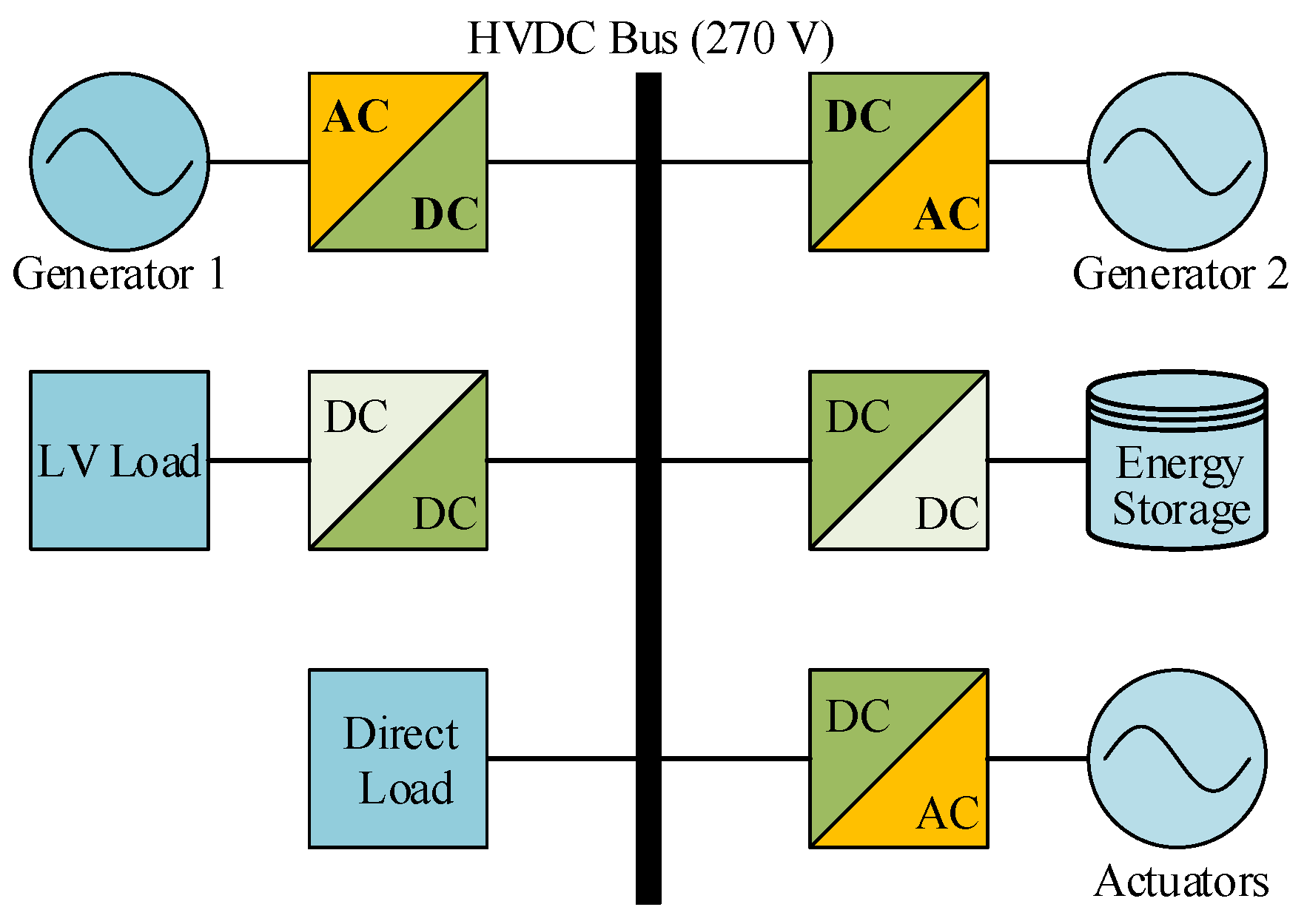
1. Introduction
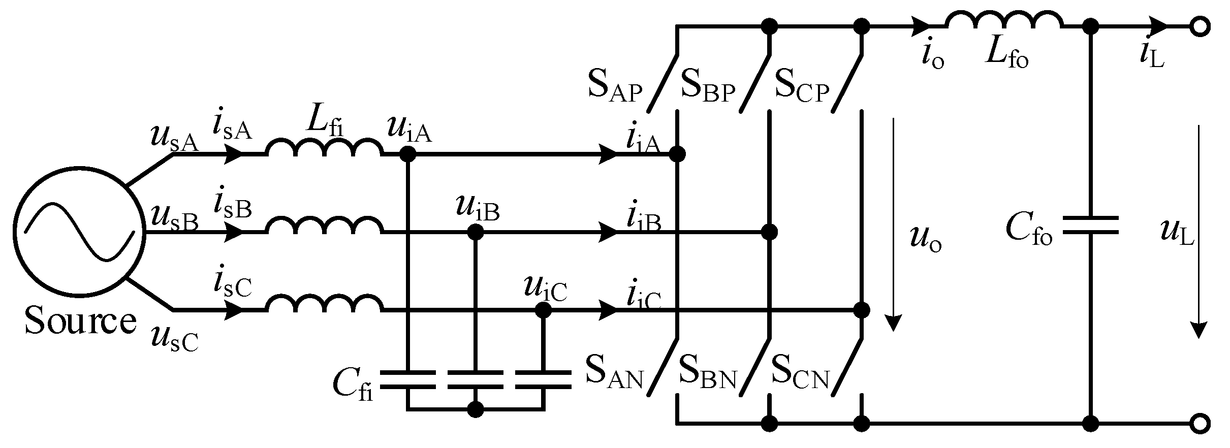
2. Mathematical Model of the CSC System
3. Proposed Hybrid Predictive Control Scheme
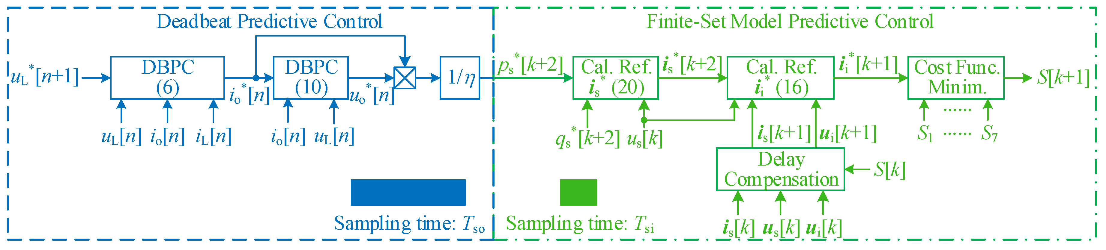
3.1. Control Block Diagram
3.2. DBPC for the Output Circuit
3.3. FS-MPC for the Input Circuit
3.4. Generation of Reference Source Currents
4. Simulation and Experimental Verification
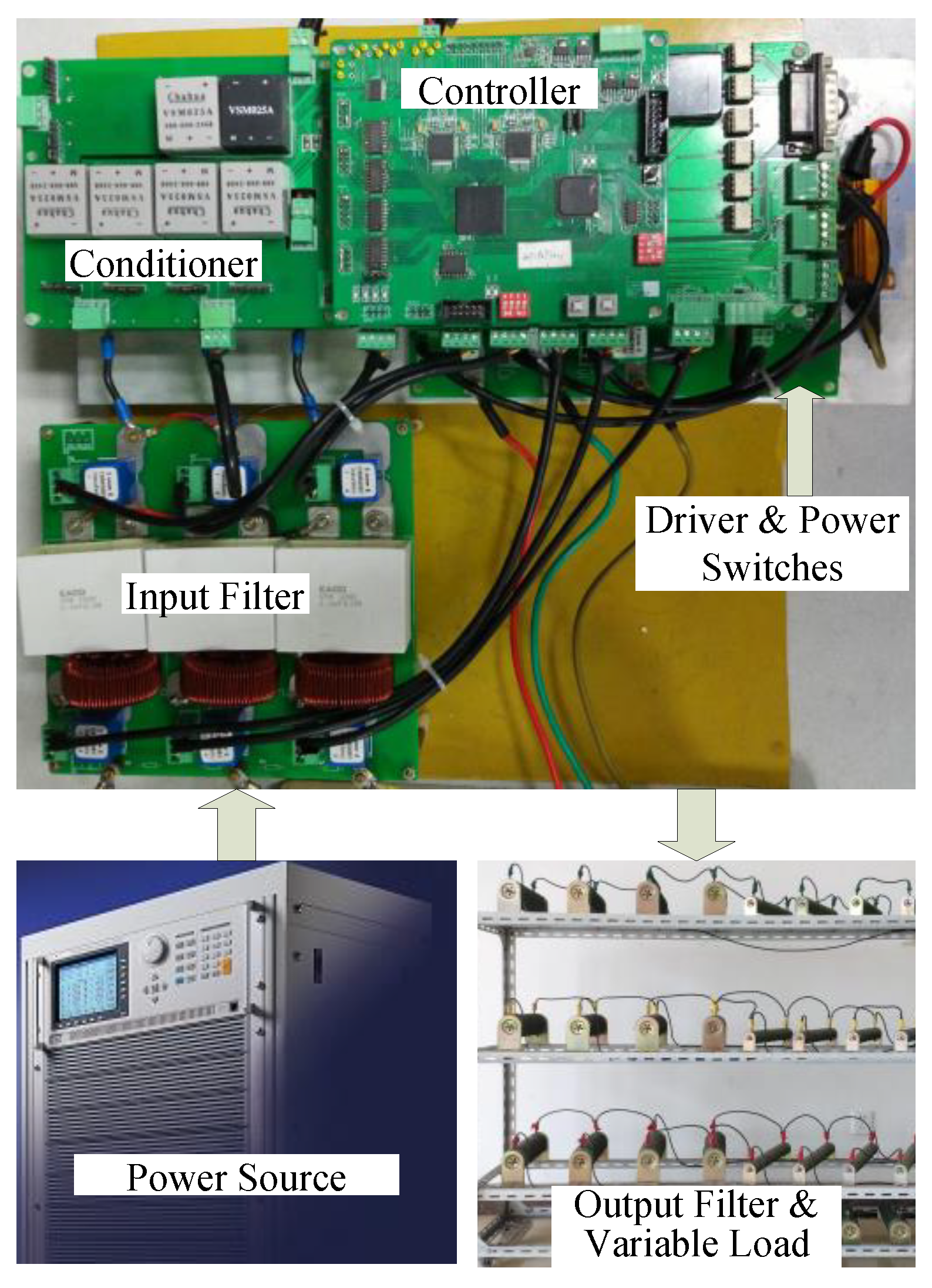
4.1. Experimental Setup
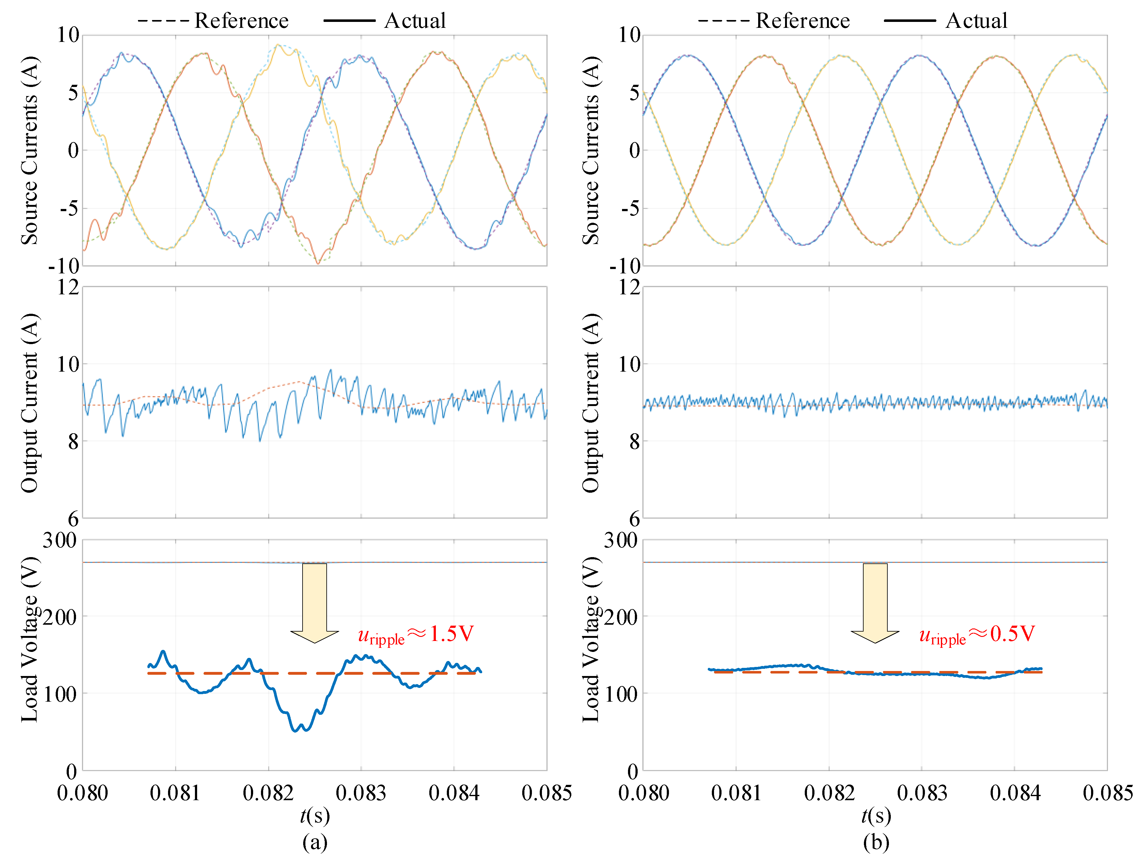
4.2. Simulation Results
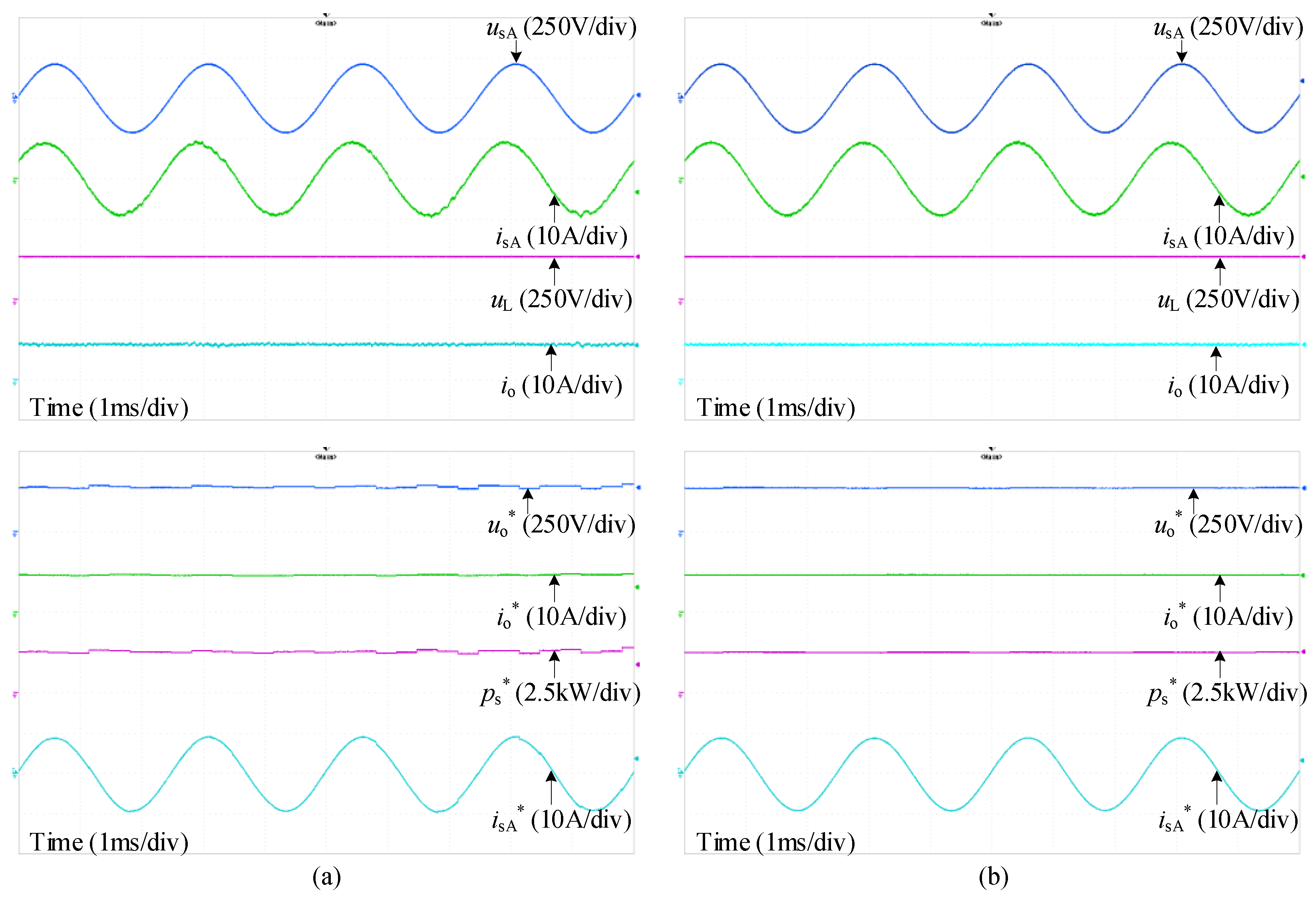
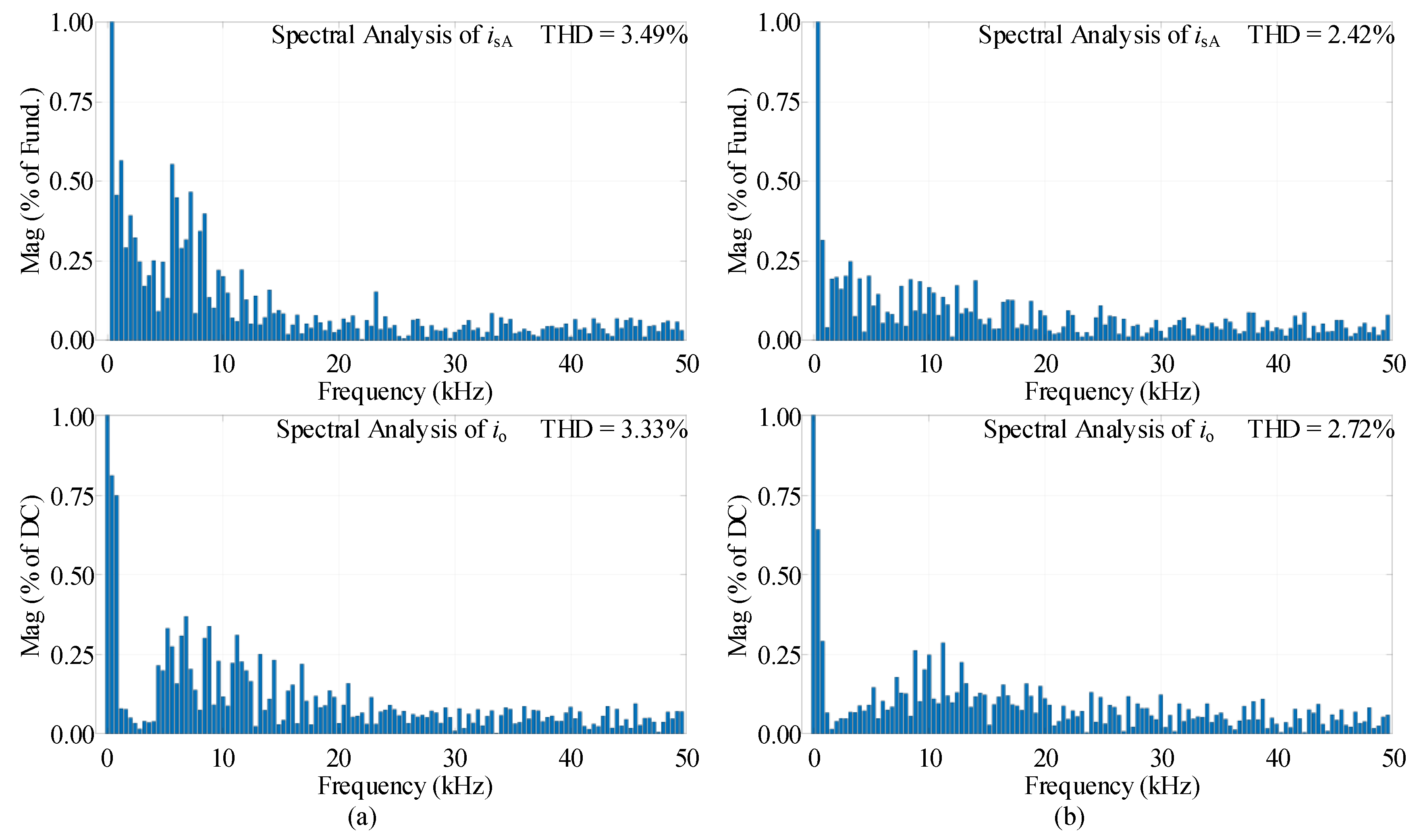
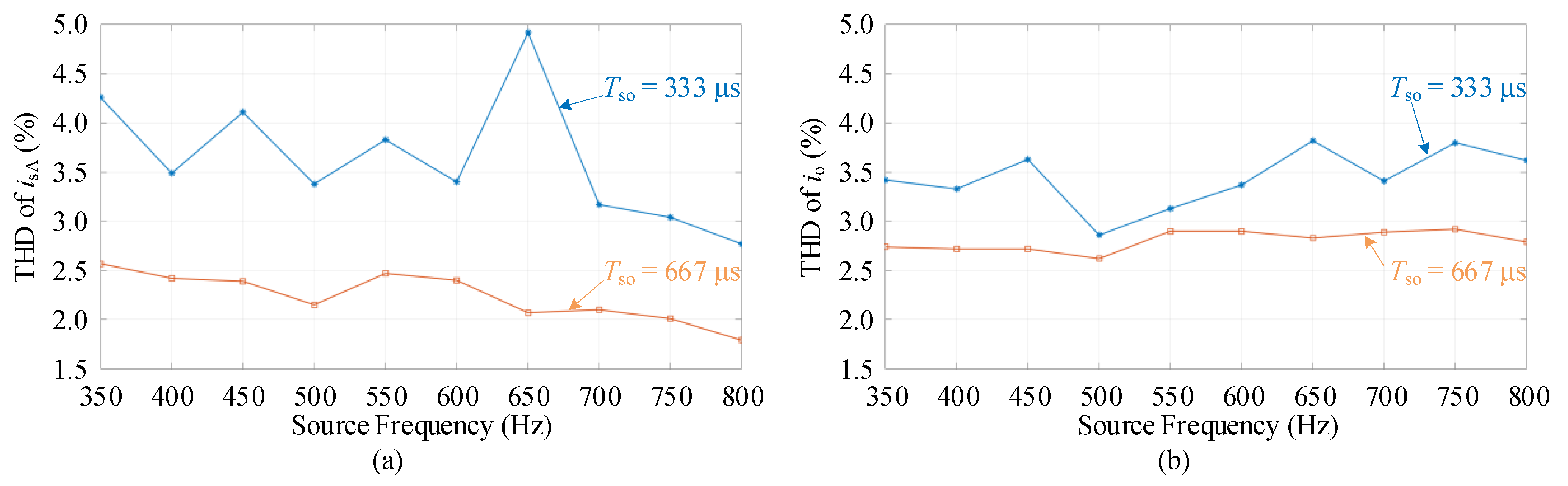
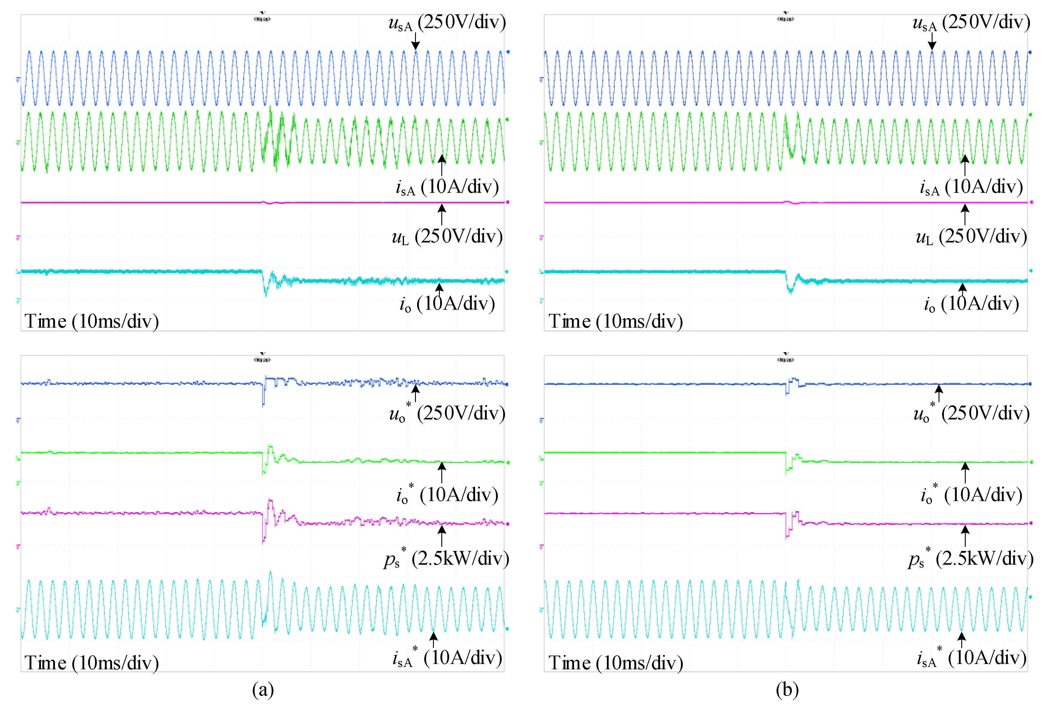
4.3. Experimental Results
5. Conclusions
Author Contributions
Funding
Conflicts of Interest
References
- Sarlioglu, B.; Morris, C.T. More Electric Aircraft: Review, Challenges, and Opportunities for Commercial Transport Aircraft. IEEE Trans. Transp. Electrif. 2015, 1, 54–64. [Google Scholar] [CrossRef]
- Buticchi, G.; Bozhko, S.; Liserre, M.; Wheeler, P.; Al-Haddad, K. On-Board Microgrids for the More Electric Aircraft—Technology Review. IEEE Trans. Ind. Electron. 2019, 66, 5588–5599. [Google Scholar] [CrossRef]
- Buticchi, G.; Costa, L.; Liserre, M. Improving System Efficiency for the More Electric Aircraft: A Look at dc/dc Converters for the Avionic Onboard dc Microgrid. IEEE Ind. Electron. Mag. 2017, 11, 26–36. [Google Scholar] [CrossRef]
- Huang, Z.; Dinavahi, V. An Efficient Hierarchical Zonal Method for Large-Scale Circuit Simulation and Its Real-Time Application on More Electric Aircraft Microgrid. IEEE Trans. Ind. Electron. 2019, 66, 5778–5786. [Google Scholar] [CrossRef]
- Yousefizadeh, S.; Bendtsen, J.D.; Vafamand, N.; Khooban, M.H.; Blaabjerg, F.; Dragičević, T. Tracking Control for a DC Microgrid Feeding Uncertain Loads in More Electric Aircraft: Adaptive Backstepping Approach. IEEE Trans. Ind. Electron. 2019, 66, 5644–5652. [Google Scholar] [CrossRef]
- Mallik, A.; Khaligh, A. An Integrated Control Strategy for a Fast Start-Up and Wide Range Input Frequency Operation of a Three-Phase Boost-Type PFC Converter for More Electric Aircraft. IEEE Trans. Veh. Technol. 2017, 66, 10841–10852. [Google Scholar] [CrossRef]
- Yin, S.; Tseng, K.J.; Simanjorang, R.; Liu, Y.; Pou, J. A 50-kW High-Frequency and High-Efficiency SiC Voltage Source Inverter for More Electric Aircraft. IEEE Trans. Ind. Electron. 2017, 64, 9124–9134. [Google Scholar] [CrossRef]
- Trentin, A.; Zanchetta, P.; Wheeler, P.; Clare, J. Performance evaluation of high-voltage 1.2 kV silicon carbide metal oxide semi-conductor field effect transistors for three-phase buck-type PWM rectifiers in aircraft applications. IET Power Electron. 2012, 5, 1873–1881. [Google Scholar] [CrossRef]
- Zhao, S.; Molina, J.M.; Silva, M.; Oliver, J.A.; Alou, P.; Torres, J.; Arévalo, F.; García, O.; Cobos, J.A. Design of Energy Control Method for Three-Phase Buck-Type Rectifier with Very Demanding Load Steps to Achieve Smooth Input Currents. IEEE Trans. Power Electron. 2016, 31, 3217–3226. [Google Scholar] [CrossRef]
- Singh, A.K.; Jeyasankar, E.; Das, P.; Panda, S.K. A Matrix-Based Nonisolated Three-Phase AC–DC Rectifier with Large Step-Down Voltage Gain. IEEE Trans. Power Electron. 2017, 32, 4796–4811. [Google Scholar] [CrossRef]
- Borovic, U.; Zhao, S.; Oliver, J.A.; Alou, P.; Cobos, J.A.; Pejovic, P. Design Methodology for Three-phase Buck-Type and Boost-Type Rectifiers to Comply with the DO-160G Current Distortion Test. IEEE Trans. Power Electron. 2019. [Google Scholar] [CrossRef]
- Nussbaumer, T.; Kolar, J.W. Advanced modulation scheme for three-phase three-switch buck-type PWM rectifier preventing mains current distortion originating from sliding input filter capacitor voltage intersections. In Proceedings of the IEEE 34th Annual Conference on Power Electronics Specialist, PESC ’03, Acapulco, Mexico, 15–19 June 2003; pp. 1086–1091. [Google Scholar] [CrossRef]
- You, K.; Xiao, D.; Rahman, M.F.; Uddin, M.N. Applying Reduced General Direct Space Vector Modulation Approach of AC–AC Matrix Converter Theory to Achieve Direct Power Factor Controlled Three-Phase AC–DC Matrix Rectifier. IEEE Trans. Ind. Appl. 2014, 50, 2243–2257. [Google Scholar] [CrossRef]
- Guo, B.; Wang, F.; Burgos, R.; Aeloiza, E. Modulation scheme analysis for high-efficiency three-phase buck-type rectifier considering different device combinations. IEEE Trans. Power Electron. 2015, 30, 4750–4761. [Google Scholar] [CrossRef]
- Afsharian, J.; Xu, D.; Wu, B.; Gong, B.; Yang, Z. The Optimal PWM Modulation and Commutation Scheme for a Three-Phase Isolated Buck Matrix-Type Rectifier. IEEE Trans. Power Electron. 2018, 33, 110–124. [Google Scholar] [CrossRef]
- Schrittwieser, L.; Cortés, P.; Fässler, L.; Bortis, D.; Kolar, J.W. Modulation and Control of a Three-Phase Phase-Modular Isolated Matrix-Type PFC Rectifier. IEEE Trans. Power Electron. 2018, 33, 4703–4715. [Google Scholar] [CrossRef]
- Vazquez, S.; Leon, J.I.; Franquelo, L.G.; Rodriguez, J.; Young, H.A.; Marquez, A.; Zanchetta, P. Model Predictive Control: A Review of Its Applications in Power Electronics. IEEE Ind. Electron. Mag. 2014, 8, 16–31. [Google Scholar] [CrossRef]
- Karamanakos, P.; Geyer, T.; Oikonomou, N.; Kieferndorf, F.D.; Manias, S. Direct Model Predictive Control: A Review of Strategies That Achieve Long Prediction Intervals for Power Electronics. IEEE Ind. Electron. Mag. 2014, 8, 32–43. [Google Scholar] [CrossRef]
- Wang, P.; Bi, Y.; Gao, F.; Song, T.; Zhang, Y. An Improved Deadbeat Control Method for Single-phase PWM Rectifiers in Charging System for EVs. IEEE Trans. Veh. Technol. 2019. [Google Scholar] [CrossRef]
- Kang, S.; Soh, J.; Kim, R. Symmetrical Three-Vector-Based Model Predictive Control with Deadbeat Solution for IPMSM in Rotating Reference Frame. IEEE Trans. Ind. Electron. 2019, 67, 159–168. [Google Scholar] [CrossRef]
- Fang, F.; Tian, H.; Li, Y. Finite Control Set Model Predictive Control for AC-DC Matrix Converter with Virtual Space Vectors. IEEE J. Emerg. Sel. Top. Power Electron. 2019. [Google Scholar] [CrossRef]
- Manoharan, M.S.; Ahmed, A.; Park, J. An Improved Model Predictive Controller for 27-level Asymmetric Cascaded Inverter Applicable in High Power PV Grid-Connected Systems. IEEE J. Emerg. Sel. Top. Power Electron. 2019. [Google Scholar] [CrossRef]
- Feng, S.; Wei, C.; Lei, J. Reduction of Prediction Errors for the Matrix Converter with an Improved Model Predictive Control. Energies 2019, 12, 3029. [Google Scholar] [CrossRef]
- Feng, S.; Lei, J.; Zhao, J.; Chen, W.; Deng, F. Improved Reference Generation of Active and Reactive Power for Matrix Converter with Model Predictive Control Under Input Disturbances. IEEE Access 2019, 7, 97001–97012. [Google Scholar] [CrossRef]
- Lei, J.; Zhou, B.; Wei, J.; Bian, J.; Zhu, Y.; Yu, J.; Yang, Y. Predictive Power Control of Matrix Converter With Active Damping Function. IEEE Trans. Ind. Electron. 2016, 63, 4550–4559. [Google Scholar] [CrossRef]
- Kiselev, A.; Catuogno, G.; Kuznietsov, A.; Leidhold, R. Finite Control Set MPC for Open-Phase Fault Tolerant Control of PM Synchronous Motor Drives. IEEE Trans. Ind. Electron. 2019. [Google Scholar] [CrossRef]
- Mardani, M.; Khooban, M.; Masoudian, A.; Dragičević, T. Model Predictive Control of DC–DC Converters to Mitigate the Effects of Pulsed Power Loads in Naval DC Microgrids. IEEE Trans. Ind. Electron. 2019, 66, 5676–5685. [Google Scholar] [CrossRef]
- Heydari, R.; Gheisarnejad, M.; Khooban, M.; Dragicevic, T.; Blaabjerg, F. Robust and Fast Voltage-Source-Converter (VSC) Control for Naval Shipboard Microgrids. IEEE Trans. Power Electron. 2019, 34, 8299–8303. [Google Scholar] [CrossRef] [Green Version]
- Correa, P.; Rodriguez, J.; Lizama, I.; Andler, D. A Predictive Control Scheme for Current-Source Rectifiers. IEEE Trans. Ind. Electron. 2009, 56, 1813–1815. [Google Scholar] [CrossRef]
- Lei, J.; Feng, S.; Wheeler, P.; Zhou, B.; Zhao, J. Steady-State Error Elimination and Simplified Implementation of Direct Source Current Control for Matrix Converter with Model Predictive Control. IEEE Trans. Power Electron. 2019. [Google Scholar] [CrossRef]
- Zavala, P.; Rivera, M.; Kouro, S.; Rodriguez, J.; Wu, B.; Yaramasu, V.; Baier, C.; Muñoz, J.; Espinoza, J.; Melin, P. Predictive control of a current source rectifier with imposed sinusoidal input currents. In Proceedings of the IECON 2013-39th Annual Conference of the IEEE Industrial Electronics Society, Vienna, Austria, 10–13 November 2013; pp. 5842–5847. [Google Scholar] [CrossRef]
- Michalik, J.; Smidl, V.; Peroutka, Z. Control approaches of current-source rectifier: Predictive control versus PWM-based linear control. In Proceedings of the IEEE PEDS, Honolulu, HI, USA, 12–15 December 2017; pp. 418–423. [Google Scholar] [CrossRef]
- Gao, H.; Wu, B.; Xu, D.; Zargari, N.R. A Model Predictive Power Factor Control Scheme With Active Damping Function for Current Source Rectifiers. IEEE Trans. Power Electron. 2018, 33, 2655–2667. [Google Scholar] [CrossRef]
- Cortes, P.; Kolar, J.W.; Rodriguez, J. Comparative evaluation of Predictive Control schemes for three-phase buck-type PFC rectifiers. In Proceedings of the 7th International Power Electronics and Motion Control Conference, Harbin, China, 2–5 June 2012; pp. 666–672. [Google Scholar] [CrossRef]
- Nguyen, T.; Lee, H. Simplified Model Predictive Control for AC/DC Matrix Converters with Active Damping Function under Unbalanced Grid Voltage. IEEE J. Emerg. Sel. Top. Power Electron. 2019. [Google Scholar] [CrossRef]

| N | SAP | SBP | SCP | SAN | SBN | SCN | ii | uo |
|---|---|---|---|---|---|---|---|---|
| 1 | 1 | 0 | 0 | 0 | 0 | 1 | (1 + 1j/)·io | −uCA |
| 2 | 0 | 1 | 0 | 0 | 0 | 1 | 2j/)·io | uBC |
| 3 | 0 | 1 | 0 | 1 | 0 | 0 | (−1 + 1j/)·io | −uAB |
| 4 | 0 | 0 | 1 | 1 | 0 | 0 | −(1 + 1j/)·io | uCA |
| 5 | 0 | 0 | 1 | 0 | 1 | 0 | −2j/·io | −uBC |
| 6 | 1 | 0 | 0 | 0 | 1 | 0 | (1 − 1j/)·io | uAB |
| 7 | 1 | 0 | 0 | 1 | 0 | 0 | 0 | 0 |
| 8 | 0 | 1 | 0 | 0 | 1 | 0 | 0 | 0 |
| 9 | 0 | 0 | 1 | 0 | 0 | 1 | 0 | 0 |
| Variables | Description | Values |
|---|---|---|
| Source | ||
| Us | Source Voltage (phase, RMS) | 150 V |
| fs | Source Frequency | 350–800 Hz |
| Input Filter | ||
| Lfi | Input Filter Inductor | 1 mH |
| Cfi | Input Filter Capacitor | 5 F |
| Rfi | Resistance of Lfi | 0.01 |
| CSC Power Setup | ||
| MOSFET | Power Switches | SCH2080KE |
| DSP | Digital Signal Processor | TMS320C28346 |
| FPGA | Field Programmable Gate Array | EP3C40F324 |
| ADC | Analog-to-Digital Converter | ADS8568 |
| DAC | Digital-to-Analog Converter | AD5754 |
| Tsi | Input Sampling Time | 6.67 s |
| Tso | Output Sampling Time | 333/667 s |
| Converter efficiency | ≈95.8% | |
| Output Filter | ||
| Lfo | Output Filter Inductor | 10 mH |
| Cfo | Output Filter Capacitor | 200 F |
| Rfo | Resistance of Lfo | 0.1 |
| Load | ||
| RL | Load Resistor | 30/45 |
| uL * | Reference load voltage | 270 V |
© 2019 by the authors. Licensee MDPI, Basel, Switzerland. This article is an open access article distributed under the terms and conditions of the Creative Commons Attribution (CC BY) license (http://creativecommons.org/licenses/by/4.0/).
Share and Cite
Yang, H.; Tu, R.; Wang, K.; Lei, J.; Wang, W.; Feng, S.; Wei, C. A Hybrid Predictive Control for a Current Source Converter in an Aircraft DC Microgrid. Energies 2019, 12, 4025. https://doi.org/10.3390/en12214025
Yang H, Tu R, Wang K, Lei J, Wang W, Feng S, Wei C. A Hybrid Predictive Control for a Current Source Converter in an Aircraft DC Microgrid. Energies. 2019; 12(21):4025. https://doi.org/10.3390/en12214025
Chicago/Turabian StyleYang, Hui, Rui Tu, Ke Wang, Jiaxing Lei, Wenjia Wang, Shuang Feng, and Chaofan Wei. 2019. "A Hybrid Predictive Control for a Current Source Converter in an Aircraft DC Microgrid" Energies 12, no. 21: 4025. https://doi.org/10.3390/en12214025
APA StyleYang, H., Tu, R., Wang, K., Lei, J., Wang, W., Feng, S., & Wei, C. (2019). A Hybrid Predictive Control for a Current Source Converter in an Aircraft DC Microgrid. Energies, 12(21), 4025. https://doi.org/10.3390/en12214025