1. Introduction
In recent years, the power system is gradually comprising more and more power sources, such as renewable energy sources and energy storage systems. Thus, multi-terminal converters have become increasingly attractive, as they can connect multiple distributed power sources instead of using several individual converters [
1,
2,
3,
4]. For example, a multi-port boost converter can collect multiple low-voltage photovoltaic outputs to achieve high-voltage output and deliver DC current to the inverter station near the load [
5,
6]. Furthermore, multi-terminal converters will play an important role in the multi-terminal HVDC grid to interconnect multiple energy sources across regions and nations [
5,
6]. In addition, in order to realize further reductions in complexity and capital cost, multi-terminal inverters with a reduced number of power semiconductor devices have been developed for the multi-motor drive systems over the past two decades [
7,
8].
Among multi-port inverters, a nine-switch inverter is a typical three-port system that can connect one DC supply to two AC loads and has the advantage of saving 25% of the number power semiconductor devices compared to using two independent inverters [
9]. However, it is limited to low and medium power applications. A modular multilevel converter (MMC) is considered the most attractive converter in high voltage applications due to its inherent features of high modularity and scalability [
10,
11,
12,
13], but it has only one output port.
The nine-arm modular multilevel converter (NA-MMC) combines the advantages of an MMC and a nine-switch inverter [
6,
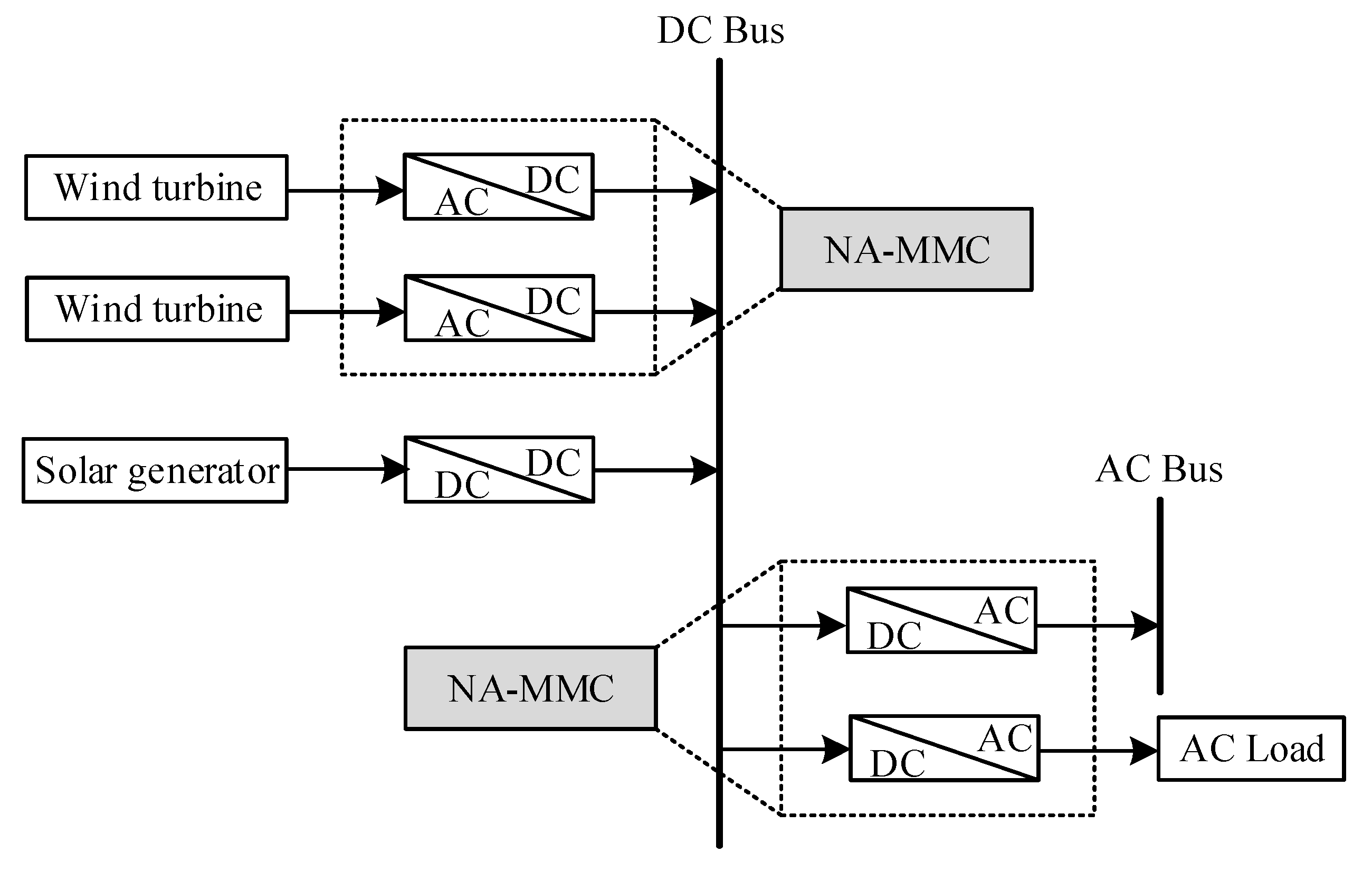
10], where each arm consists of sub-modules in series, rather than a single switch. Thus, it can reduce the number of power semiconductor devices, compared to using two separate MMCs, and can operate in high-voltage occasions. In the case shown in
Figure 1 [
14,
15], one NA-MMC is used to connect the DC bus, the AC bus, and an AC load which has different frequency and/or amplitude from the nearby AC bus. Another NA-MMC is used to connect the outputs of two different wind turbines to the DC bus. Thus, an NA-MMC can be applied in many medium/high voltage multi-terminal systems.
It is known that the pole-to-pole DC fault will impose major restrictions on MMC, especially for overhead transmission lines [
16,
17]. As a multi-terminal converter has more than two terminals, its DC-side fault phenomena is more complex than that of a traditional MMC. There are usually two main approaches to assist MMCs with handling DC-side faults. One is to employ a DC circuit breaker (CB) with relatively high let-through current to isolate the DC fault current in a short time after the DC side fault occurs. However, the availability of DC CBs are restricted due to their high cost and imperfections [
18,
19]. The other approach is to use sub-modules with DC fault handling capabilities [
19,
20,
21]. For example, by replacing the half-bridge sub-module (HBSM) with the full-bridge sub-module (FBSM) in the NA-MMC, a reverse voltage can be generated by the FBSM capacitors to block the short-circuit current subsequent to the DC-side fault. Obviously, if the NA-MMC is composed of FBSM, it will have the a DC-fault blocking capability. Nevertheless, the number of power semiconductor devices in FBSMs is twice that of power semiconductor devices in HBSMs [
22]. This not only increases the cost of NA-MMC systems, but also brings larger power losses as the current passes two power semiconductor devices in each FBSM instead of one in each HBSM. Thus, the configuration scheme based on FBSM only manages the fault condition and sacrifices the cost and efficiency. To pursue the optimal design in terms of DC-fault blocking capability, efficiency, and cost, the hybrid design concept making use of HBSM and FBSM has been put forward [
23].
Therefore, the contributions of this paper are as follows: (1) To construct a hybrid nine-arm high-voltage inverter with HBSMs and FBSMs, (2) to analyze all types of fault current in the multi-terminal inverter, and (3) to obtain the optimal ratio of HBSM and FBSM in the different arms.
The rest of this paper is organized as follows.
Section 2 introduces the topology and operating principle of the proposed hybrid nine-arm high-voltage inverter.
Section 3 analyzes all potential short-circuit current paths and the corresponding DC fault blocking scheme of the proposed hybrid inverter.
Section 4 provides the simulation results to demonstrate the feasibility and effectiveness of the proposed hybrid inverter.
Section 5 draws the conclusions.
2. Topology and Operating Principle
2.1. Basic Configuration
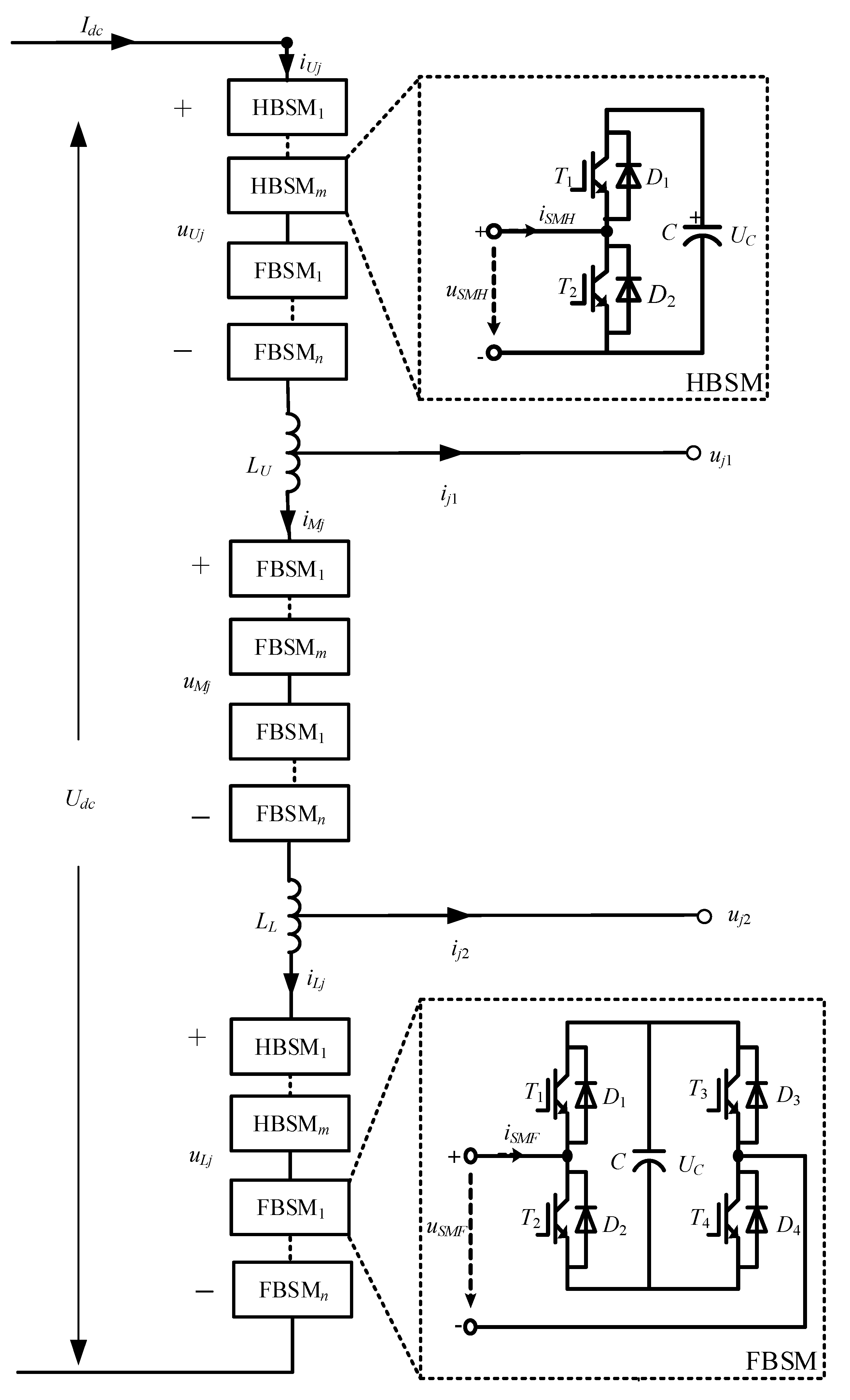
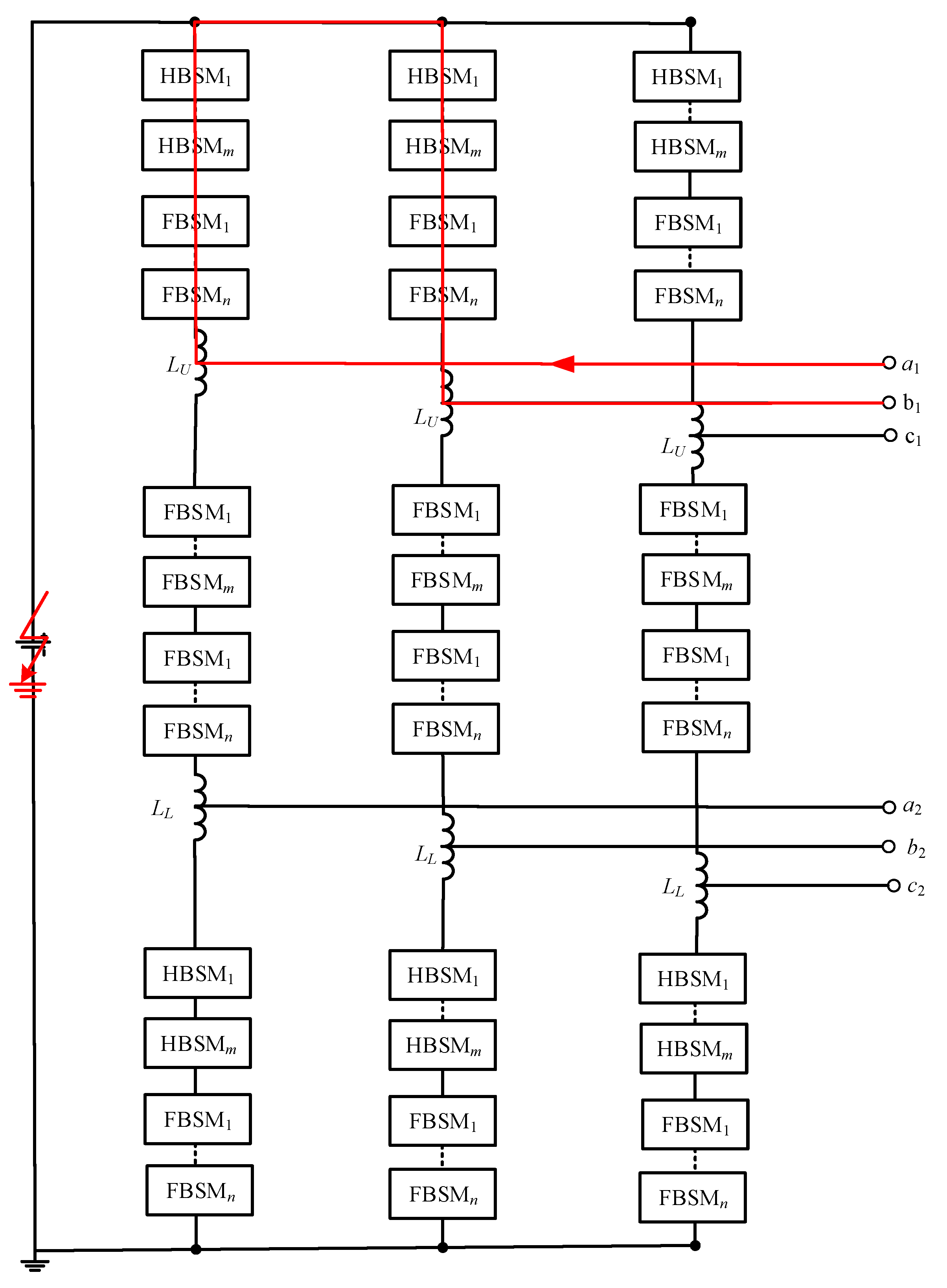
Figure 2 shows one phase of the hybrid nine-arm high-voltage inverter with a DC fault blocking capability. The upper and lower arms are composed of
m HBSMs and
n FBSMs, but the middle arm is composed of
FBSMs. Every sub-module (SM) can be considered as a controlled voltage source, for which output voltage is determined by the ON/OFF states of power switches.
Inductors LU and LL are two buffer inductors, with . The value is the DC-link voltage and is the DC-side current. The value is the capacitor voltage of SM and equals to . The values , and are the currents of upper arm, middle arm, and lower arm in phase j (), respectively. The values , and are the voltages of upper arm, middle arm, and lower arm in phase j, respectively. The values and are the output voltages of the inverter upper port and lower port of phase j, while and are the corresponding output port currents.
Based on the structure of HBSM shown in
Figure 2, the output voltage of HBSM,
, is decided by the ON/OFF states of switches
and
, and the driving signals of
and
are complementary. When
is ON,
is equal to the capacitor voltage
. When
is ON,
is equal to 0. Similarly, the output voltage of FBSM
depends on the ON/OFF states of
to
, which is
,
, or 0.
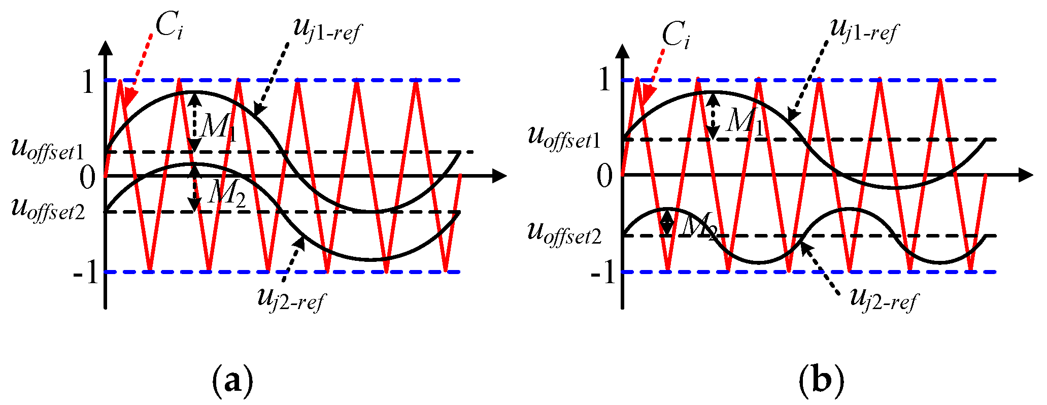
2.2. Modulation Scheme
Like the NA-MMC, the hybrid nine-arm high-voltage inverter can also be controlled by carrier phase-shifted pulse-width modulation (CPS-PWM), in which N triangular carriers are compared with two modulating references to obtain the driving signals for SMs. The triangular carriers are shifted in an angle of 360/N, where N is the total number of SMs in each arm and .
Assume that the modulating references of dual AC outputs are expressed as follows:
where
and
are fundamental angular frequencies of dual AC outputs
and
,
and
are modulation ratios,
and
are relative phases,
and
are appropriate offsets, and
θ is 0 when
,
when
, and
when
.
The hybrid nine-arm high-voltage inverter has two operating modes. When
, the inverter is working in common frequency (CF) mode. In another situation (
), the inverter is working in different frequency (DF) mode. The relationship among the upper reference,
, the lower reference,
, and carrier signal,
, under CF and DF modes are shown in
Figure 3. The amplitudes of
and
cannot exceed the range of the carrier, so then we have
. As the upper modulating reference,
, should always be greater than the lower modulating reference,
, to avoid overlap [
10],
and
must be satisfied in CF mode, while
must be satisfied in DF mode.
Based on the CPS-PWM method for the NA-MMC [
10], the gate signals for the
ith SM in upper, middle, and lower arms (
,
and
) can be obtained by comparing the
ith carrier signal
(where
i = 1, 2, …,
N) to the reference signals
and
, which are shown in
Figure 3 and
Figure 4. It can be found that
is the positive logic value generated by
and
,
is the negative logic value generated by
and
, and
is the logical exclusive OR (XOR) value of
and
, that is,
.
2.3. Basis Operation
According to Reference [
10], the upper and lower AC voltages,
and
, are determined by
where
,
, and
are the voltages of the upper, middle and lower arm, respectively.
The arm voltage is known to be the sum of SM output voltages on the arm. With the CPS-PWM scheme [
24],
,
, and
can be controlled to
Substituting (3) into (2), and are expressed as
2.4. Operation Under DC Fault Condition
After a pole-to-pole DC fault occurs, the DC side current is raised rapidly and the load on the AC side will inject energy into the DC side through the hybrid inverter. If the hybrid inverter does not provide a large enough reverse voltage to prevent the injected energy, then an AC side current will flow directly to the DC side fault point due to the freewheeling effect of the anti-parallel diode of the sub-module and the DC fault will turn to an AC fault.
The DC fault blocking capability of the proposed hybrid nine-arm high-voltage inverter is achieved by inhibiting the gate signals to the SMs after the DC fault is detected.
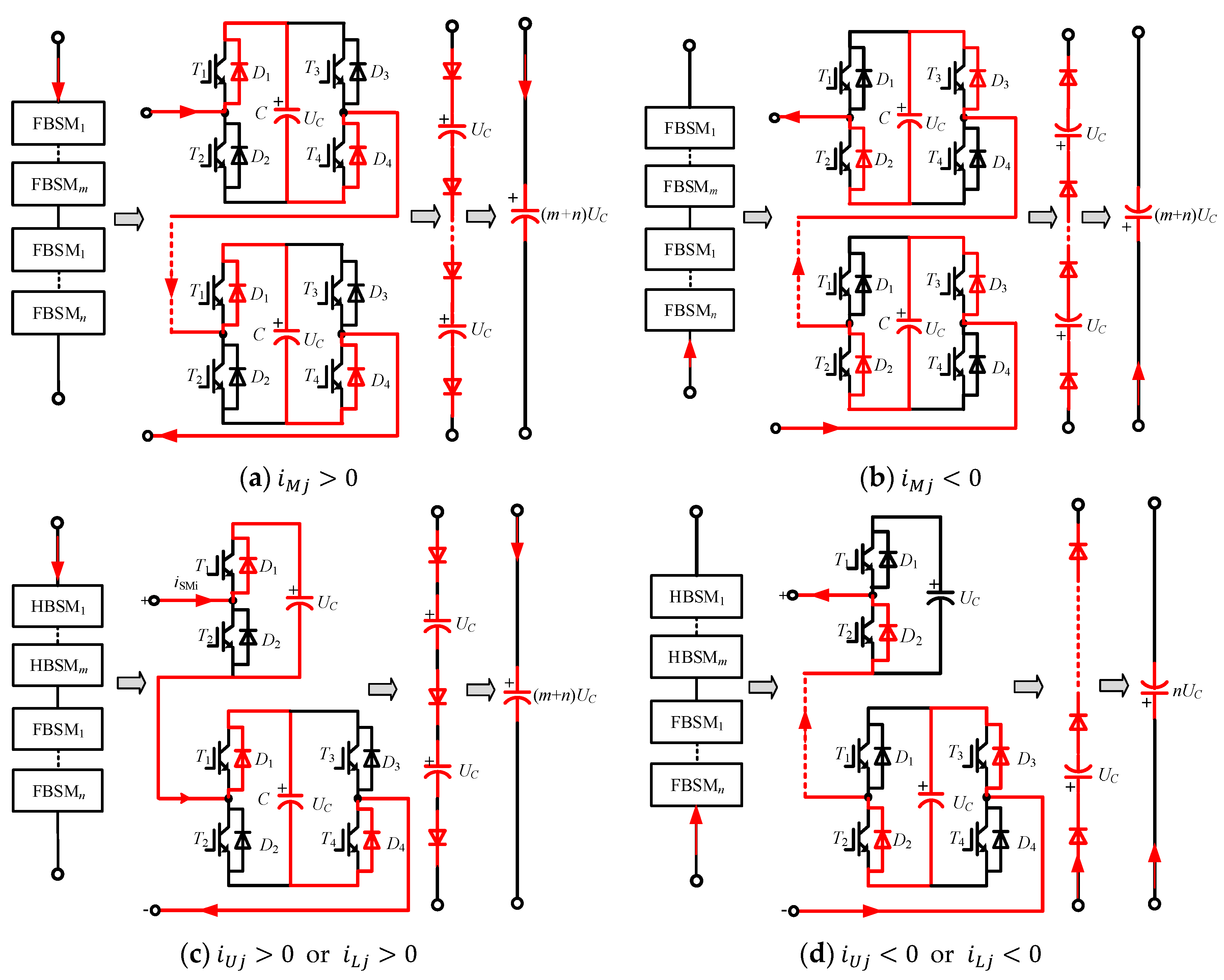
Figure 5 shows the equivalent circuits of different arms when all insulated gate bipolar transistors (IGBTs) in SMs are turned off, which turn out to be diodes in series with SM capacitors. If the formed series voltage is larger than the AC side voltage, then the fault current will be interrupted within a very short time.
3. DC Fault Blocking Scheme
The hybrid nine-arm high-voltage inverter can connect to two AC loads with different frequencies and amplitudes. When the DC side fault occurs, the AC sides will feed the current to the fault point through arms. The possible fault current paths of the hybrid nine-arm high-voltage inverter are shown in
Figure 6, where
,
, and
are the upper AC ports and
,
, and
are the lower AC ports.
After the DC side fault occurs, drops to zero rapidly and increases sharply. When the current is detected to be greater than the current threshold, it can be judged that there is a short circuit fault in the system, then all the IGBTs of the inverter receive the turn-off signals to protect the SMs. After all of the IGBTs are turned off, the short circuit current can be formed between different output ports and the DC side. In order to reduce the fault currents, a sufficiently large reverse voltage must be provided in the fault current flow path. All types of possible current flow paths in the hybrid nine-arm high-voltage inverter are analyzed in order to obtain the total reverse voltage that should be provided.
3.1. Different Ports with the Middle Arm
The fault current path shown in
Figure 7 is formed by the middle arm of the inverter. Although this current path does not pass through the DC side when a short-circuit fault occurs on the DC side, a large current will be generated between the different ports through the middle arm of the converter, which may damage the inverter.
Take the upper output port and the lower output port as the example. Assume that and . The voltage difference between two output ports is
Then the maximum voltage between the two ports is
It is known that the maximum voltage between the output ports
and
is smaller than
. Assume that there are
m HBSMs and
n FBSMs in the middle arm, based on
Figure 5, the voltage formed by the capacitors in series will be
when the fault current flows from
to
, or
when the fault current flows from
to
. In order to keep the fault current under control in any case,
should be satisfied. Hence, there is no need to use HBSM to meet the requirement of fault current blocking and the middle arm can be composed of FBSMs only. In order to make the number of sub-modules the same as that of the upper and lower arms, there must be
FBSMs in the middle arm. This is the main reason why the ratio of HBSM to FBSM in the middle arm is different from the other two arms in the proposed hybrid nine-arm high-voltage inverter.
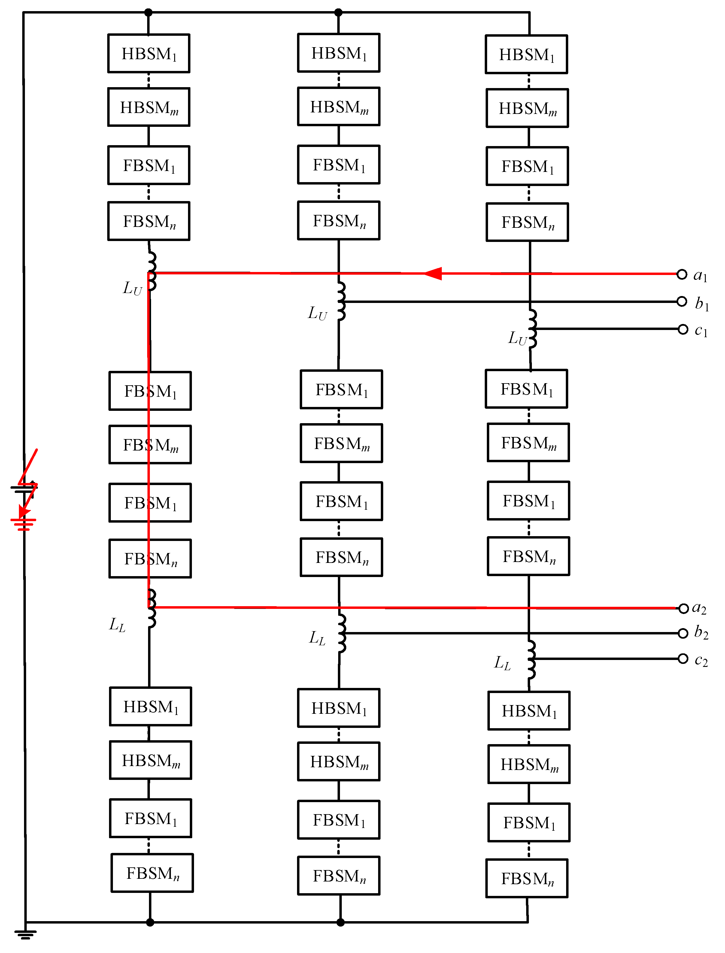
3.2. Different Ports with the DC-Side
The fault current path shown in
Figure 8 is formed by the upper output port, the DC side, and the lower output port. When a short-circuit fault occurs on the DC side, the AC side inputs energy to the DC side through the different arms of the inverter.
Take the upper output port and the lower output port as the example. Assume that , and , the voltage difference between two output ports is
No matter if it is in CF mode () or DF mode (), the maximum magnitude of is
That is, the maximum voltage between two AC ports of
and
is
. As there are
FBSMs and
HBSMs in this path, the voltage formed by FBSMs and HBSMs on this path is
, according to
Figure 5c,d. The total capacitor voltage
is greater than
because
. Therefore, any relationship between
m and
n in this case can keep the possible fault current under control.
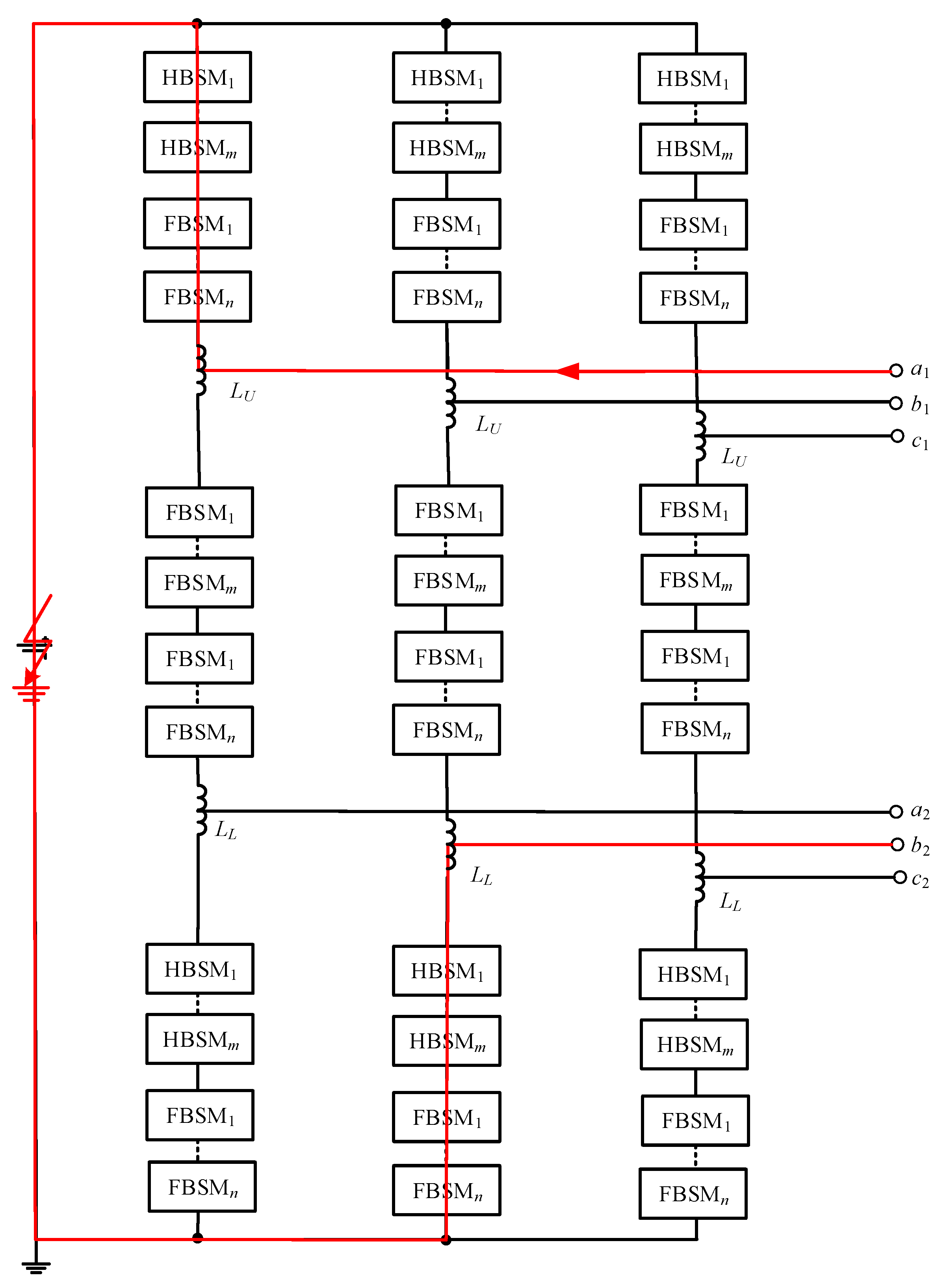
3.3. Same Port of the Different Phase
The fault current path shown in
Figure 9 is formed by the two upper (lower) output ports and the upper (lower) arm of the different phase. This type of fault current does not pass through the DC side, but a large current can also be generated between the different ports through the upper or lower arms.
Take the upper output port and the other upper output port as the example. Assuming that , , and , the voltage difference between these two ports is
Then the maximum magnitude of is
Based on
Figure 5c,d, the voltage formed by SMs in this path is
, or
, since the capacitor voltage of each SM is controlled to be
, which is absolutely larger than
. In order to control the cost and to maintain the ability of DC fault self-cleaning,
is the most suitable ratio for the upper and lower arms.
The characteristics of the HBSM based nine-arm inverter (HBSM based NA inverter), the FBSM based high-voltage nine-arm inverter (FBSM based NA Inverter), and the proposed hybrid nine-arm inverter (Hybrid NA inverter) are summarized in
Table 1.
4. Simulation Results
To verify the operating scheme and theoretical analysis of the hybrid nine-arm high-voltage inverter presented in this paper, a simulation model of the proposed inverter, which has the same configuration as shown in
Figure 2, was set up in MATLAB/SIMULATION. The parameters of the simulation model are listed in
Table 2.
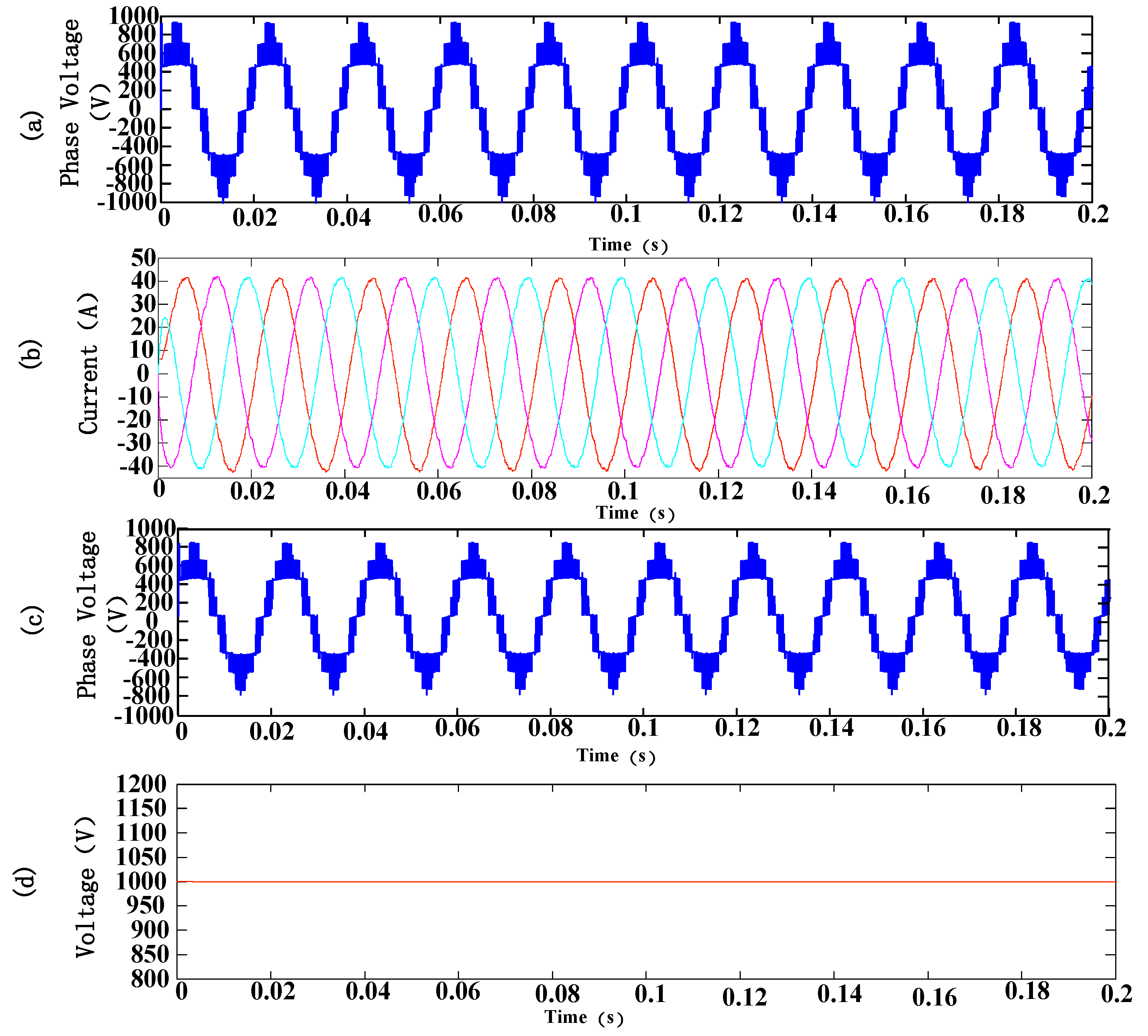
Some key waveforms of the proposed hybrid nine-arm high-voltage inverter are shown in
Figure 10.
Figure 10a,c shows the line-to-line voltages of the upper and lower output ports, respectively.
Figure 10b shows the three-phase current of the upper output port and
Figure 10d shows the DC side voltage of the proposed inverter.
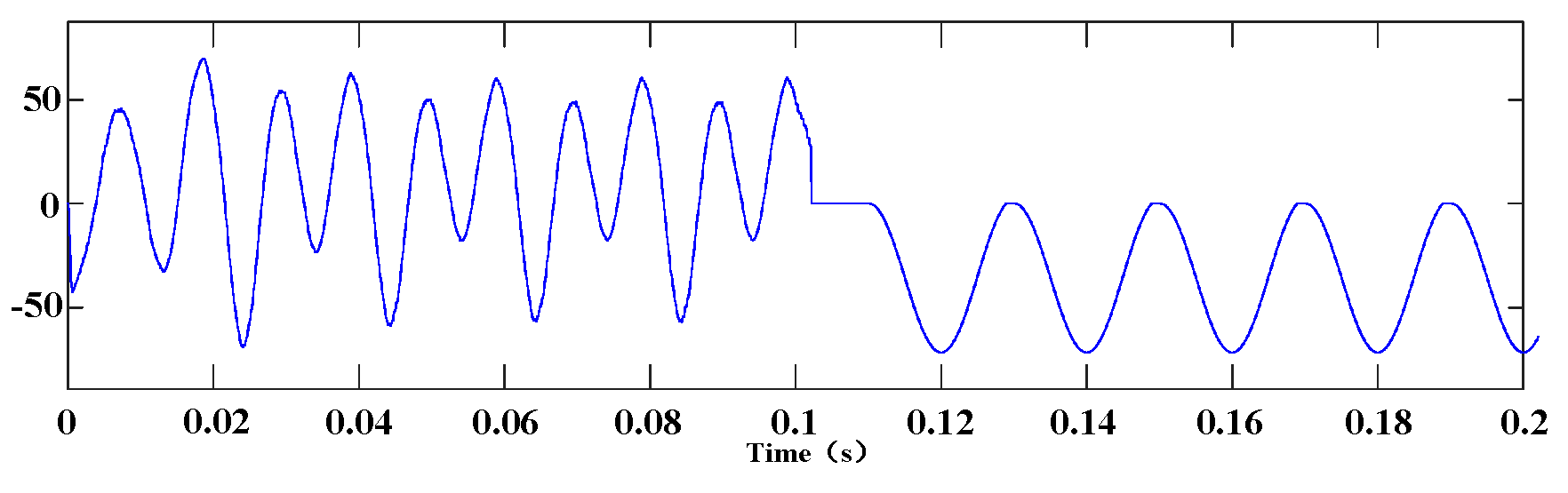
In order to prove the above three fault current paths and verify the ability to clear DC fault, the hybrid nine-arm high-voltage inverter is tested by momentarily changing the DC-side voltage to zero. After the DC fault occurs, the hybrid nine-arm high-voltage inverter takes no actions and keeps operation as normal state.
Assuming that the hybrid nine-arm high-voltage inverter is in normal operation before 0.1s and the DC fault occurs at 0.1s,
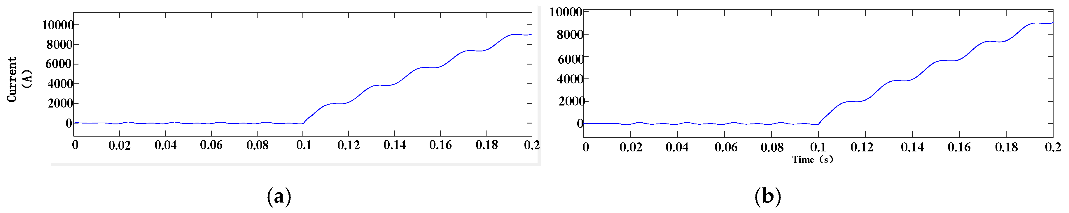
Figure 11 shows the current of middle arm, of which the direction is the same as in
Figure 7.
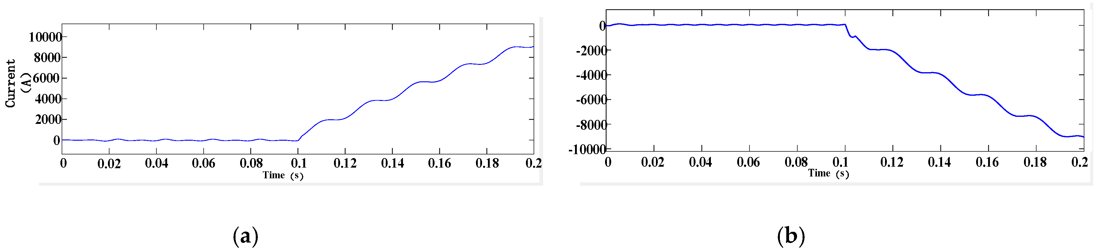
Figure 12 shows the current waveforms of the upper arm and lower arm when the fault current path in
Figure 8 is generated.
Figure 13 shows the current waveforms of different upper arms when the fault current flows in the path shown in
Figure 9. It can be seen from these figures that the fault current increases at a very high speed after the DC fault occurs and the AC side continuously delivers energy to the inverter. The large fault current will damage the inverter if no protective measures are taken after 0.1 s.
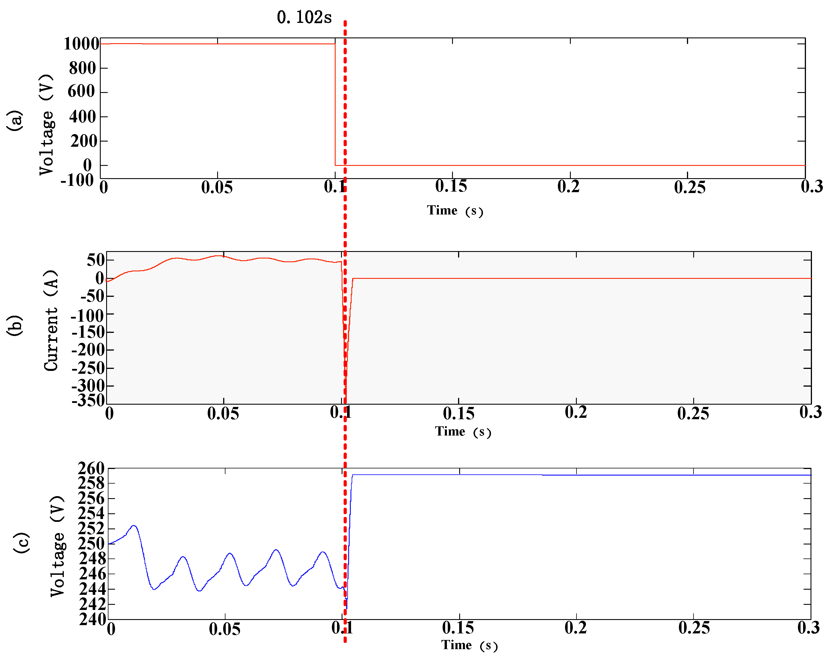
When the DC fault happens, the DC side voltage
drops to 0 immediately, as shown in
Figure 14a. The proposed hybrid nine-arm high-voltage inverter still maintains the operating state as before at the first several milliseconds, the energy from the AC side and capacitors feed back to the DC side, then both the DC side and AC side currents increase, as shown in
Figure 14b. The fault current flows through the capacitors in the FBSMs and causes its voltage to increase slightly, as seen in
Figure 14c. Assume that all the IGBTs of the proposed hybrid inverter are turned off at 0.102 s. Since the total series voltage formed by the SM capacitors in the fault current flow path is greater than the AC voltage, the arm current quickly reduces to zero, then there is no energy exchange between the DC side and the AC side. After the DC fault is cleared, no current flows through the capacitors and the capacitor voltage remains unchanged.
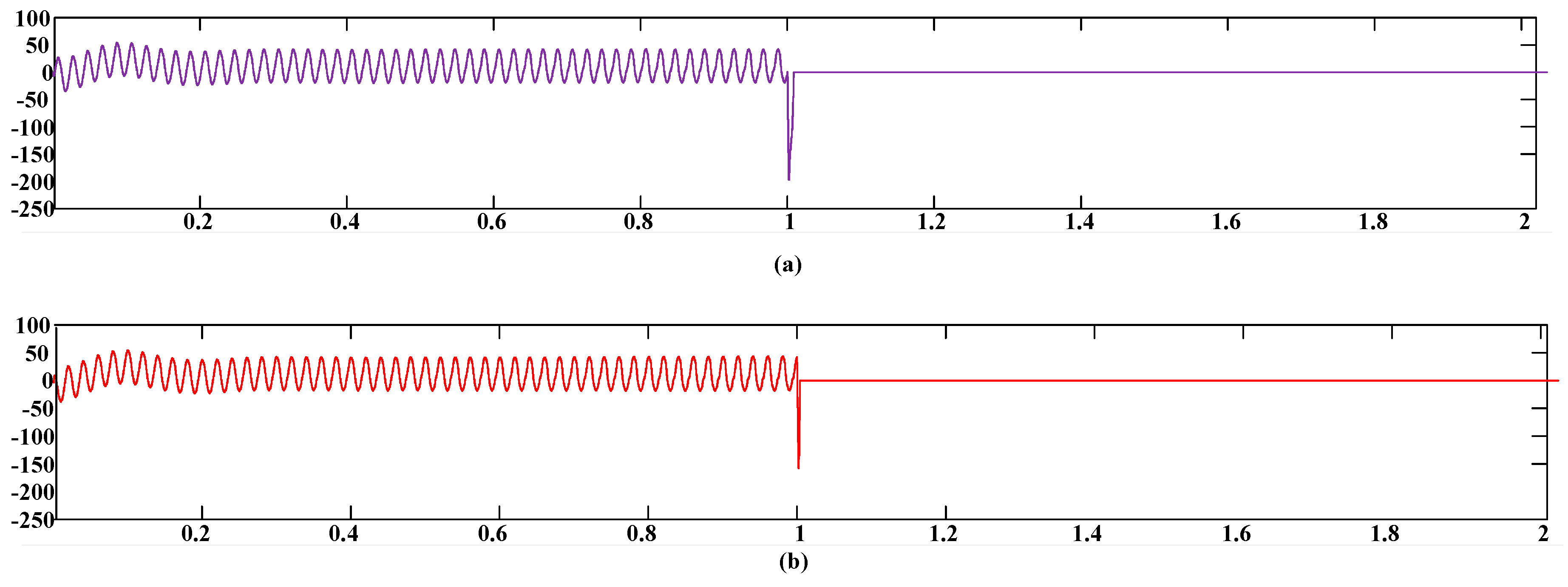
Figure 15 shows the upper arm currents of phase
a and phase
c with the peak values 197 A and 157 A, respectively. In fact, the fault current will not exceed the preset current threshold. Obviously, the above simulation results prove that the proposed hybrid nine-arm high-voltage inverter has the DC fault blocking capability.


