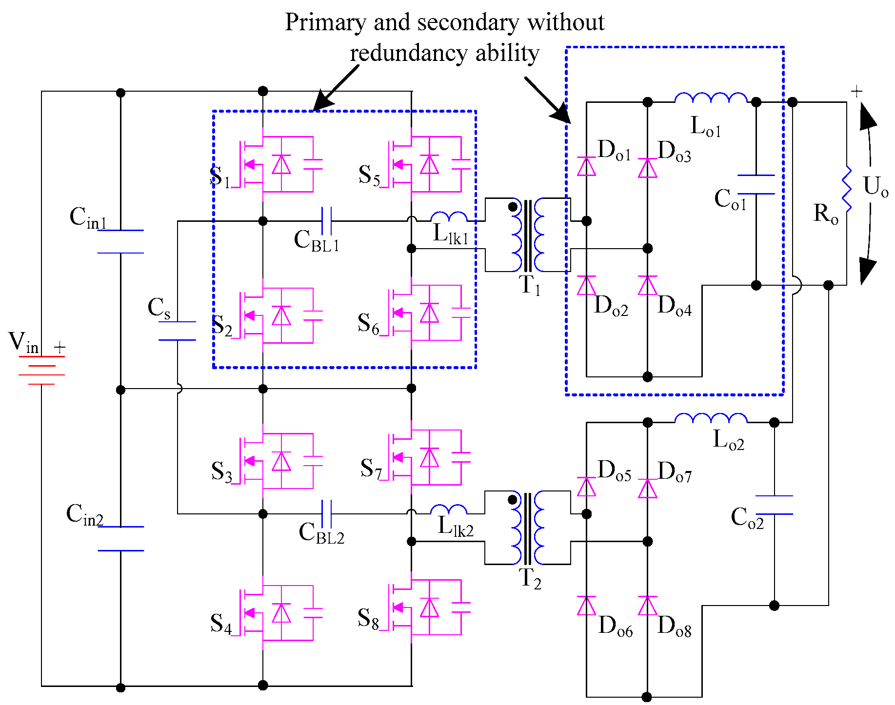
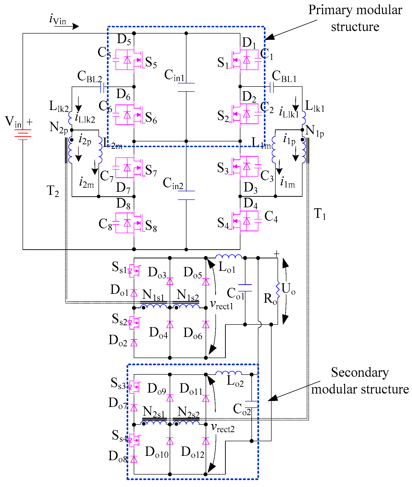
Before the discussion, some assumptions are concluded as follows: (1) the on-resistance of the primary switches are neglected; (2) the voltage ripple on C
in1, C
in2, C
BL1 and C
BL2 can be neglected due to high capacitance; (3) the output capacitance of the power devices is identical, and is represented by C
o; (4) L
lk1 and L
lk2 are identical, and are represented by L
lk; (5) L
1m and L
2m are identical, and are represented by L
m; (6) N
1p is identical to N
2p, and N
1s1 = N
1s2 = N
2s1 = N
2s2; (7)
kT = N
1p/N
1s1 = N
2p/N
2s1; (8) the current ripple of
iLo1 and
iLo2 is neglected; (9) With proper controlling, the output currents of the two paralleled connected modules can be identical, and the controlling method is not discussed in this paper. Therefore,
iLo1 =
iLo2.
iLo1 and
iLo2 are represented by I
o ; (10)
iin is identical to
iVin +
iCin, and its AC content is defined as
. During the normal operation, the proposed converter can be controlled in the secondary side and primary side modulation modes.
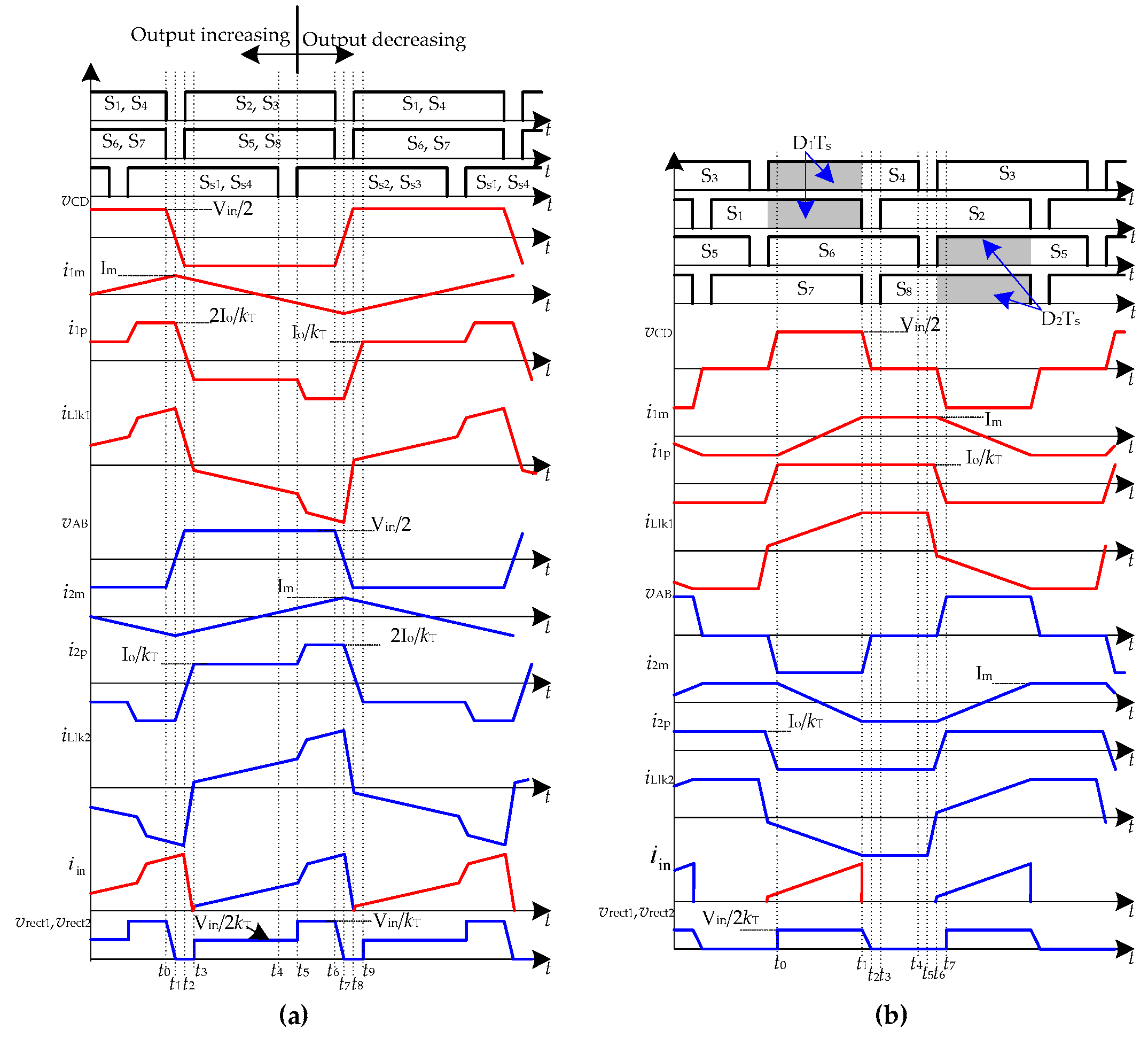
Figure 3 depicts the key waveforms,
Table 1 and
Table 2 show the switching status in each stage.
3.1. Secondary Side Modulation
As shown in
Figure 3a, the primary switches can be divided into two groups. The first group is S
1, S
4, S
6 and S
7; while another group is S
2, S
3, S
5 and S
8. The switches in each group are switched ON and OFF synchronously, and the switches in different groups are switched in the complementary mode. In the secondary side, S
s2 and S
s3 are switched ON and OFF synchronously; while S
s1 and S
s4 are switched ON and OFF synchronously. S
s1 and S
s3 are switched in the complementary mode with S
s2 and S
s4. V
o can be regulated by the phase angel between gate signals of S
s1 and S
1, S
s3 and S
5. When these angles equal 180°, V
o = V
in/(2k
T). There are 12 operation stages in one switching cycle, and the operation stages in the first half switching cycle are illustrated in
Figure 4.
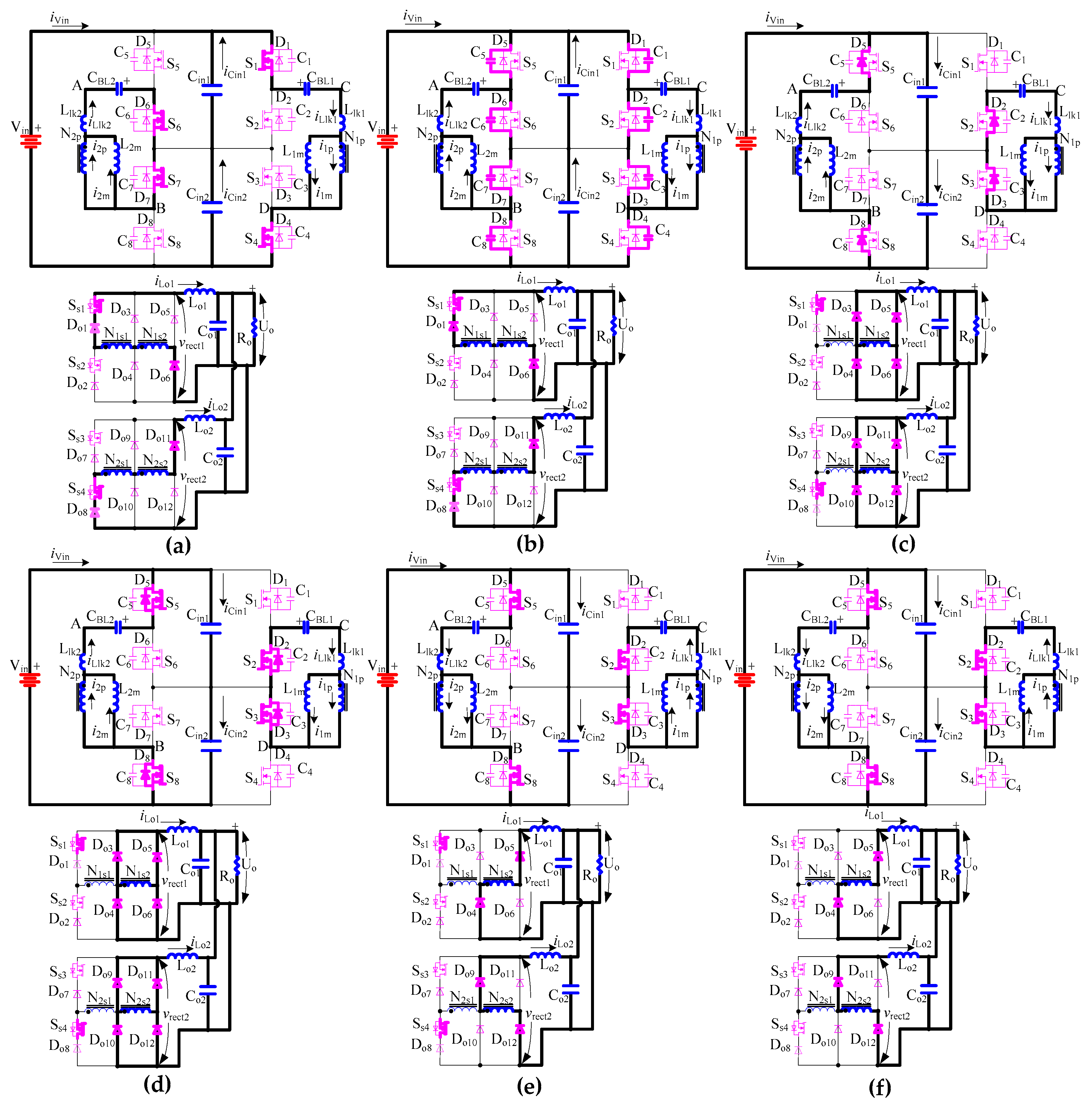
Stage 1 [
Figure 4a]: before t
0, the circuit is stable. Input source powers the load. In the primary side, S
1, S
4, S
6 and S
7 are ON; v
CD = V
in/2, and v
AB = −V
in/2;
i1p = 2I
o/
kT, and
i2p = −2I
o/
kT.
iLlk1 and
iLlk2 are
iin =
iVin +
iCin1 with the value of
iLlk1. The DC content of
iin flows from the input source to the primary sides of the transformers directly.
iCin1 is partial AC content of
iin depends on the reactance distribution of the input source and input capacitors. As
iCin1 is identical to
iCin2, the midpoint voltage of C
in1 and C
in2 is constant during this period. v
S2 and v
S5 are clamped by C
in1, and v
S3 and v
S8 are clamped by C
in2.
In the secondary side, Ss1 and Ss4 are ON; Do1, Do6, Do8 and Do11 are conducted; vrect1 = vrect2 = Vin/kT.
Stage 2 [
Figure 4b,
t0-
t1]: At
t0, S
1, S
4, S
6 and S
7 are switched OFF. In the primary side, the slope rates of
i1m and
i2m are very slow, and the absolute value of these currents is constant value I
m. Therefore, the absolute value of
iLlk1 and
iLlk2 during this period is
iLlk1 charges C
1 and C
4, discharges C
2 and C
3; while
iLlk2 charges C
6 and C
7, discharges C
5 and C
8.
vS1,
vS4,
vS6 and
vS7 are
vS2,
vS3,
vS5 and
vS8 are
According to (4) and (5), the voltage of S1-S8 is lower than Vin/2, before the end of this stage.
This stage lasts until
vS1 is V
in/2, and the interval is
iCin1 is identical to
iCin2, which is
iLlk1−
iLlk2, and under ideal condition, this value is zero. Therefore, the midpoint voltage of C
in1 and C
in2 can also be stabled during this period.
In the secondary side, Ss1 and Ss4 are ON; Do1, Do6, Do8 and Do11 are conducted; vrect1 = vrect2 = 2vCD(t)/kT = 2|vAB (t)|/kT.
Stage 3 [
Figure 4c,
t1-
t2]: At
t1, D
2, D
3, D
5 and D
8 are ON. In the primary side,
vCD = −V
in/2, and
vAB = V
in/2; L
1m and L
2m sustain negative voltage, and
i1m and
i2m are
iLlk1 and
iLlk2 are
iin =
iVin +
iCin1 with the value of
iLlk2. The DC content of
iin will flow from the input source to the primary sides of the transformers directly.
iCin1 is partial AC content of
iin depends on the reactance distribution of the input source and input capacitors. As
iCin1 is identical to
iCin2, the midpoint voltage of C
in1 and C
in2 is constant during this period.
vS1 and
vS6 are clamped by C
in1, and
vS4 and
vS7 are clamped by C
in2. S
2, S
3, S
5 and S
8 should be gated after
t1 to achieve ZVS operation.
In the secondary side, Do3-Do6 and Do9-Do12 are ON to free-wheel the secondary currents. vrect1 = vrect2 = 0.
Stage 4 [
Figure 4d,
t2-
t3]: At
t2, S
2, S
3, S
5 and S
8 are switched ON with ZVS. In the primary side,
i1m,
i2m,
i1p and
i2p keep increasing in the reverse direction, and the increasing slope are defined as (13) to (16).
iin =
iVin +
iCin1 with the value of
iLlk2.
iCin1 is partial AC content of
iin depends on the reactance distribution of the input source and input capacitors. As
iCin1 is identical to
iCin2, the midpoint voltage of C
in1 and C
in2 is constant during this period.
vS1 and
vS6 are clamped by C
in1, and
vS4 and
vS7 are clamped by C
in2.
In the secondary side, Do3-Do6 and Do9-Do12 are conducted to free-wheel the secondary currents. Ss1 and Ss4 are ON. As the currents through Ss1 and Ss4 are 0, thus, Ss1 and Ss4 can achieve ZCS turned on after this period. vrect1 and vrect2 are zero.
Stage 5 [
Figure 4e)
t3-
t4]: At
t3, the absolute value of
i1p and
i2p is I
o/
kT. In the primary side, S
2, S
3, S
5 and S
8 are ON;
vCD =−V
in/2, and
vAB = V
in/2;
i1p = −I
o/
kT, and
i2p = I
o/
kT.
i1m and
i2m are
iLlk1 and
iLlk2 are
iin =
iVin +
iCin1 with the value of
iLlk2.
iCin1 is partial AC content of
iin depends on the reactance distribution of the input source and input capacitors. As
iCin1 is identical to
iCin2, the midpoint voltage of C
in1 and C
in2 is constant during this period.
vS1 and
vS6 are clamped by C
in1, and
vS4 and
vS7 are clamped by C
in2.
In the secondary side, Do4, Do5, Do9 and Do12 are conducted; vrect1 = vrect2 = Vin/(2kT).
Stage 6 [
Figure 4f,
t4-
t5]: At
t4, S
s1 and S
s4 are OFF with zero-current switching (ZCS). After
t5, the circuit will be operated into the secondary switching period, and detail analyses are not provided here for the sake of simplicity.
The ideal output-input voltage ratio in this mode is
3.2. Primary Side Modulation
When the phase angle between S
s1 and S
1 is 180°, the secondary side modulation mode cannot further change the output voltage. To regulate output voltage down to zero, the converter must be controlled into the primary side modulation mode. In this mode, the secondary switches S
s1-S
s4 are OFF; the primary switches are divided into two groups, which are S
1 to S
4 and S
5 to S
8. As shown in
Figure 3b, the primary switches in each group are switched in the PS switching scheme, and S
1 and S
6 are switched with the same phase angle. D
1 and D
2 are duty ratios of S
1-S
4 and S
5-S
8, and with symmetrical switching pattern, D
1 = D
2. The output voltage is varied with the value of D
1 and D
2, when D
1 = D
2 = 0, the output voltage is zero. The key waveforms of this mode are depicted in
Figure 3b, and the operation stages in the first half switching cycle are illustrated in Figure 6.
Stage 1 [
Figure 5a]: before
t1, the circuit is operated in steady condition. Input source powers the load. In the primary side, S
1, S
4, S
6 and S
7 are ON;
vCD = V
in/2, and
vAB =−V
in/2;
i1p = −I
o/
kT, and
i2p = I
o/
kT.
iLlk1 and
iLlk2 are
iin =
iVin +
iCin1 with the value of
iLlk1.
iCin1 is formed by partial AC content of
iin depends on the reactance distribution of the input source and input capacitors. As
iCin1 is identical to
iCin2, the midpoint voltage of C
in1 and C
in2 is constant during this period.
vS2 and
vS5 are clamped by C
in1, and
vS3 and
vS8 are clamped by C
in2.
In the secondary side, Ss1-Ss4 are OFF; Do3, Do6, Do10 and Do11 are conducted; vrect1 = vrect2 = Vin/(2kT).
Stage 2 [
Figure 5b,
t1-
t2]: At
t1, S
1 and S
7 are switched OFF. In the primary side, S
1 and S
7 can obtain zero-voltage turned OFF due to existence of C
1 and C
7.
i1m and
i2m reach their maximum absolute value I
m. Therefore, the absolute values of
iLlk1 and
iLlk2 are
iLlk1 charges C
1, discharges C
2; while
iLlk2 charges C
7, discharges C
8.
vS1 and
vS7 are
According to (19) and (20), vS1, vS2, vS7 and vS8 is lower than Vin/2 before the end of this stage.
This stage ends until
vS1 and
vS7 is V
in/2, and the time is
iCin1 is identical to iCin2, which is iLlk1-iLlk2, and with symmetrical switching sequence iCin1 is zero. Therefore, the midpoint voltage of Cin1 and Cin2 is constant during this period.
In the secondary side, Do3, Do6, Do10 and Do11 are conducted; vrect1 = vrect2 = vCD(t)/kT = |vAB (t)|/kT.
Stage 3 [
Figure 5c,
t2-
t4]: At
t2, D
2 and D
8 are on. In the primary side,
vCD =
vAB = 0;
i1m and
i2m keep constant value I
m;
i1p and
i2p are with the same absolute value |I
o/
kT|, During this period,
iLlk1 and
iLlk2 are
iCin1 is identical to
iCin2 with the value of
iLlk1-
iLlk2, thus, with symmetrical switching cycle,
iCin1 and
iCin2 are zero, which means stable midpoint voltage of input capacitors can be achieved. Therefore, the midpoint voltage of C
in1 and C
in2 is constant during this period.
vS1 and
vS5 are clamped by C
in1, and
vS3 and
vS7 are clamped by C
in2. S
2 and S
8 should be gated after
t2 to achieve ZVS operation, and according to
Figure 3b, S
2 and S
8 are switched at
t3.
In the secondary side, Do3-Do6 and Do9-Do12 are ON to free-wheel the secondary currents. vrect1 = vrect2 = 0.
Stage 4 [
Figure 5d,
t4-
t5]: At
t4, S
4 and S
6 are switched OFF. In the primary side, S
4 and S
6 can obtain zero-voltage turned OFF due to C
4 and C
6. The primary currents keep constant during this stage.
iLlk1 charges C
4, discharges C
3; while
iLlk2 charges C
6, discharges C
5.
vS4 and
vS5 are
This stage ends until
vS4 and
vS6 are V
in/2, and the time is
iCin1 is identical to iCin2 with the value of iLlk1-iLlk2, thus, with symmetrical switching cycle, the currents flowing through Cin1 and Cin2 are zero, which means stable midpoint voltage of input capacitors can be achieved. Therefore, the midpoint voltage of Cin1 and Cin2 is constant during this period.
In the secondary side, Do3-Do6 and Do9-Do12 are ON to free-wheel the secondary currents. vrect1= vrect2 = 0.
Stage 5 [
Figure 5e,
t5-
t6]: At
t5, D
3 and D
5 are ON. In the primary side,
vCD = −V
in/2, and
vAB = V
in/2; negative voltage is applied on magnetic inductors, and
i1m and
i2m are
iLlk1 and
iLlk2 are
iin =
iVin +
iCin1 with the value of
iLlk2.
iCin1 is partial AC content of
iin depends on the reactance distribution of the input source and input capacitors. As
iCin1 is identical to
iCin2, the midpoint voltage of C
in1 and C
in2 is constant during this period.
vS1 and
vS6 is clamped by C
in1, and
vS4 and
vS7 is clamped by C
in2. S
3 and S
5 should be gated after
t5 to achieve ZVS operation, and according to
Figure 3b, S
3 and S
5 are switched at
t6.
In the secondary side, Do3-Do6 and Do9-Do12 are ON to free-wheel the secondary currents. vrect1 = vrect2 = 0.
Stage 6 [
Figure 5f,
t6-
t7]: At
t7,
i1p equals −I
o/
kT, and
i2p equals I
o/
kT; the free-wheeling mode is over. Input source powers the load. In the primary side, S
2, S
3, S
5 and S
8 are ON;
vCD =−V
in/2, and
vAB = V
in/2.
iin =
iVin +
iCin1 with the value of
iLlk1.
iCin1 is partial AC content of
iin depends on the reactance distribution of the input source and input capacitors. As
iCin1 is identical to
iCin2, the midpoint voltage of C
in1 and C
in2 is constant during this period.
vS1 and
vS3 are clamped by C
in1, and
vS4 and
vS7 are clamped by C
in2.
In the secondary side, Ss1-Ss4 are OFF; Do4, Do5, Do9 and Do12 are conducted; vrect1 = vrect2 = Vin/(2kT).
The ideal output-input voltage ratio in this mode is


