Article

Sliding Mode Control of the Isolated Bridgeless SEPIC High Power Factor Rectifier Interfacing an AC Source with a LVDC Distribution Bus

by
Oswaldo Lopez-Santos
1,*,
Alejandro J. Cabeza-Cabeza
1,
Germain Garcia
2 and
Luis Martinez-Salamero
3
1
Facultad de Ingeniería, Universidad de Ibagué, Carrera 22 Calle 69 Barrio Ambalá, 730001 Ibagué, Colombia
2
Laboratoire d’Analyse et d’Architecture des Systèmes, Centre Nationale de Recherche Scientifique (LAAS-CNRS), Institut National des Sciences Appliquées (INSA), 7 Avenue du Colonel Roche, 31077 Toulouse, France
3
Departament d’Enginyeria Electrònica, Elèctrica i Automàtica, Universitat Rovira i Virgili, Av. Paisos Catalans, No. 26, 43007 Tarragona, Spain
*
Author to whom correspondence should be addressed.
Energies 2019, 12(18), 3463; https://doi.org/10.3390/en12183463
Submission received: 2 July 2019 / Revised: 4 September 2019 / Accepted: 6 September 2019 / Published: 7 September 2019
(This article belongs to the Special Issue Sliding Mode Control of Power Converters in Renewable Energy Systems)

Abstract

:
This paper deals with the analysis and design of a sliding mode-based controller to obtain high power factor (HPF) in the bridgeless isolated version of the single ended primary inductor converter (SEPIC) operating as a single-phase rectifier. In the work reported here, the converter is used as a unidirectional isolated interface between an AC source and a low voltage direct current (LVDC) distribution bus. The sliding-mode control is used to ensure the tracking of a high quality current reference at the input side, which is obtained from a sine waveform generator synchronized with the grid. The feasibility of the proposal is validated using simulation and experimental results, both of them confirming a reliable operation and showing good static and dynamic performances.

Graphical Abstract

1. Introduction

The use of rectifiers operating with high power factor (HPF) is a mandatory issue today in AC-DC conversion [1]. This fact reduces the negative impact on the power quality of AC distribution networks caused by the increasing introduction of new energy processing technologies such as electric mobility and efficient lighting, among others. For example, hybrid electric vehicles need battery chargers, which must not only provide high power density and plug-and-play operation [2], but also meet the requirements of the power quality international standards. In the same context, it is possible to integrate the HPF rectification function in multi-mode converters, which can provide bidirectional power transfer capability or multiple power conversion types (AC-DC, DC-DC, and DC-AC), which eventually has an important impact on the power density of the converter in the electric vehicle [3]. At lower power levels, HPF rectifiers allow improving the input power quality and the general performance of LED lamps, which currently constitute the leading lighting technology in the market [4].
Utilization of HPF rectifiers is also fundamental in the newest applications related to feeding DC loads [5], DC distribution, and microgrids. On the basis of the high efficiency and flexibility of the low voltage direct current (LVDC) distribution systems [6], HPF rectifiers take part of the main DC source because they incorporate control systems that can help to meet the strict requirements of grid compatibility, safety [7], and power quality [8]. This type of power distribution is also currently integrated in microgrids, which constitutes a popular research topic in several industrial electronics areas [9]. Hybrid or AC-DC microgrids are extensively used and are supplied from renewable resources such as photovoltaic and wind, besides AC sources, namely, either the AC mains, electric machines, or fuel generators [10]. Although bidirectional power flow is a desired feature in many applications, unidirectional power flow is efficiently used in wind power integration, speed regulation, plug-in electric vehicles, and other two-quadrant applications [11]. In all cases, it is intended that the AC powered devices accomplish the international power quality standards in terms of total harmonic distortion (THD) and power factor [12].
The HPF rectifiers can be classified in a simple way as isolated and non-isolated. Non-isolated topologies, in turn, can be classified regarding the use of diode bridges. In particular, if a topology does not require one or more diode bridges, it is denominated bridgeless [13]. The bridgeless topologies generally exhibit a better performance because the number of semiconductor elements in a circulating current path is low. The conventional bridgeless single ended primary inductor converter (SEPIC) was presented by Ismail et al. [14], providing the basis for subsequent works developed by the same authors. This converter was studied in the work of [15] in discontinuous conduction mode (DCM), which resulted in a relatively simple control and a reduced size of the components at the expense of increased stress in semiconductors. More recently, in the works of [16,17], the bridgeless SEPIC rectifier topology was modified by adding multiplier cells in order to extend the operational input voltage range. Although the efficiency in the work of [16] was considerably improved (values above 98%), no increased performance was reported in the power quality indicators such as THD and power factor.
Although galvanic isolation between the AC source and DC distribution bus is not a mandatory issue in HPF rectifiers, it is clear that this feature can contribute to improving the system reliability, especially when the use of DC distribution buses implies the interconnection of multiple sources, different loads, and ancillary elements. For that reason, there is a particular interest in the development of HPF rectifiers with isolated topologies. For example, in the works of [18,19], an isolated rectifier topology is obtained by means of a special configuration of low-frequency transformers (Scott transformer), in which two separated bridge rectifiers based on either boost or buck converters are used to feed a split DC-bus. In another paper [20], isolation is obtained by integrating two isolated Cûk rectifiers configuring a bridgeless topology. A relevant feature of that configuration is the use of coupled inductors operating at high frequency, which eventually results in a significant improvement in the cost, size, and weight of the converter in comparison with the use of low-frequency transformers.
Different isolated architectures based on the SEPIC converter have been proposed in the literature for HPF rectifiers. An interesting alternative with interleaved configuration and a bridge- based SEPIC rectifier topology is presented in the work of [21], attaining unity power factor for a wide range of the output voltage. Nonetheless, the reported THD increases up to nearly 10% for some operation conditions. The isolation in that case is provided by a second conversion stage based on an LLC converter. Also, an active clamp topology operating in both continuous conduction mode (CCM) and DCM has been reported another paper [22], showing an acceptable performance at the expense of an additional input filter and high current stress in semiconductors. The three-phase architecture of isolated SEPIC rectifier presented in the work of [23] uses three high- frequency transformers and three bridge-based bidirectional switches, improving the performance of the single-phase bridgeless SEPIC rectifier. In the latter work, DCM operation is used to obtain a THD of 4% and unity power factor. However, the mentioned parameters were not evaluated in the entire range of operation rated for the converter. It is worth mentioning that the resulting efficiency in the aforementioned cases ranges from 75% to 90%.
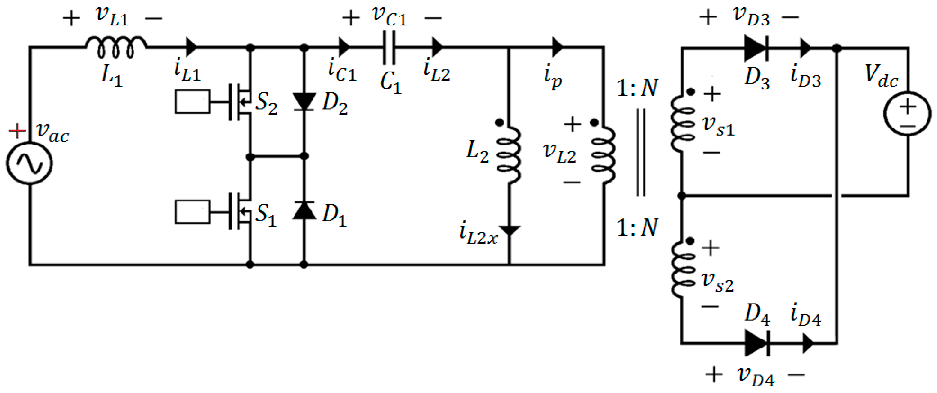
The bridgeless configuration of the HPF SEPIC rectifier depicted in Figure 1 has been presented in the work of [24], working at constant switching frequency, which is imposed by a pulse width modulation (PWM) operation in the control loop. Besides the galvanic isolation, the authors of that work have highlighted the relatively low number of components and the low levels of resulting Electro Magnetic Interference (EMI) as the main advantages of the topology. The main features in the isolated version of the SEPIC converter are as follows: (i) the existence of a series inductor in the input port imposing a continuous behavior to the input current, (ii) the capability to either step-up or step-down the input voltage, and (iii) the enhancement of the input voltage range with respect to other topologies.
The control of HPF rectifiers based on the SEPIC converter can be easily implemented using continuous-time linear methods and PWM. The wave-shaping, as defined by Tanitteerapan et al. in the literature [25,26], leads to low values of THD, while a good reference generation method allows achieving power factor correction. This is carried out by an inner control loop that normally processes the input current and is complemented by an outer loop regulating the output voltage in the case of rectifiers operating as pre-regulators. In addition, discrete-time control techniques such as repetitive control have been applied to control the SEPIC rectifier [27]. With this technique, the THD is high at low power levels, but enters in the permissive range for 50% of the nominal power, which suggests that there is still an important gap to improve the rectifier performance in terms of THD. Besides, in the work of [28], a linear control approach is compared with a feedback linearization technique, demonstrating a better performance of the linear technique in power factor and THD for nominal power. The nonlinear technique shows a slightly advantageous performance by regarding the THD distribution along the whole range of the converter power. In the same work, the robustness of the control system is improved by applying an adaptive passivity-based feedback linearization approach.
Sliding-mode control (SMC) has been also applied to control the SEPIC rectifier using a PWM implementation [29]. The power factor obtained with this technique in always higher than 0.97, while the current THD is only lower than 5% around the nominal power. It can be observed again that the decrease of the THD is an open problem in the SEPIC rectifier.
SMC using a hysteresis implementation results in variable switching frequency, but offers robustness, fast response, reliability, and simple implementation using either analog or digital electronics. It has been demonstrated that this technique is able to track periodic references, forcing loss-free resistor behavior. This implies resistive behavior at the input port and power source behavior at the output port of a power converter [30], which in fact transforms the set rectifier-load into a virtual resistance, as it is successfully developed for a semi-bridge-less pre-regulator in the work of [31] and a three-phase HPF Vienna rectifier in the work of [32]. As in the case of the grid-connected inverters, the control must track a reference, which can be directly provided by a measurement of the input voltage or indirectly by a synchronized reference generator [33]. On the other hand, as the output voltage of the rectifier (voltage of the DC bus) is not regulated, the power injected into the DC bus is given by the amplitude of the input current. This amplitude is in turn provided by an outer control loop that can be a part of a high-level layer of hierarchical control architectures [34].
The main goal of this work is to apply a hysteresis-based implementation of the sliding mode control approach to improve the performance of the isolated SEPIC converter, increasing the range of power in which the international standards are fulfilled.
Unlike the approach in the work of [24], the SEPIC converter analyzed in this paper feeds a non-resistive load and operates at a variable switching frequency. The first constraint has not been studied in any of the reported SEPIC-based rectifier topologies. More specifically, the main differences of the topology depicted in Figure 1 with respect to the conventional SEPIC are as follows:
-
The single controlled switch was changed by a bidirectional switch ( S 1 / D 1 , S 2 / D 2 ) providing control for voltage and current in both half-cycles of the grid voltage.
-
A transformer with three windings, the first one being the primary, replaces the second inductor. The secondary is split in two identical windings, which are interconnected through a central tap. The transformer ratio is 1:N.
-
No output capacitor is used because the converter is directly connected to a voltage regulated DC bus.
Moreover, this paper considers the sliding mode-based current control of a bridgeless isolated SEPIC rectifier tracking a sinusoidal reference and injecting power to an LVDC bus without considering additional control outer loops. The rest of the paper is organized as follows. Modeling and analysis of the sliding-mode current control are developed in Section 2. The implementation of the proposed control is described in Section 3. Simulation and experimental results are shown in Section 4. Finally, conclusions are given in Section 5.

2. Converter Model and Control

2.1. Detailed Description of the Converter

As can be observed in Figure 1, the converter is fed by the AC source v a c , while the distribution bus is represented by the constant DC source V d c . The converter is composed by controlled switches S 1 and S 2 ; diodes D 1 , D 2 , D 3 , and D 4 ; capacitor C 1 ; and inductors L 1 and L 2 . The latter element is a coupled inductor with three windings, one primary ( n 1 turns) and two identical secondary windings ( n 2 = n 3 turns), which are represented in the figure by inductance L 2 and an ideal transformer with ratio N = n 2 / n 1 = n 3 / n 1 . The voltage at the primary side of the coupled inductor is denoted as v L 2 , while the voltage at the secondary windings is defined as v s 1 and v s 2 , respectively.
The operation of the converter as a HPF rectifier is accomplished by means of the controlled switches S 1 and S 2 commutating at high frequency along each half-cycle of the AC source and the natural switching of diodes D 3 and D 4 , which are connected to the secondary windings of the transformer at the output of the converter. To correctly ensure a safe operation of S 1 and S 2 , D 1   and   D 2   are activated and deactivated simultaneously with S 2 and S 1 , respectively.
The isolated SEPIC rectifier in CCM [35] exhibits four possible configurations, that is, two for the positive half-cycle of v a c and two for the negative one. Also, the proposed circuit can operate in an additional configuration during the zero crossings of the AC input. In that configuration, the input side of the converter can be represented by a single mesh with both inductors L 1 and L 2 in series with capacitor C 1 , like in a series resonant converter. The control signal u takes the values 0 or 1 during the off and on states of the controlled switches, respectively. Variable a will allow us to distinguish operation in CCM ( a = 0 ) and the operation in the above-mentioned additional configuration ( a = 1 ).
During the positive half-cycle, in the on state (Figure 2a), inductor L 1 is directly connected to the source v a c through the path composed by S 1 and D 2 , while capacitor C 1 is directly connected to L 2 , while the DC source V d c is disconnected from the secondary because D 3 and D 4 are open. In the off-state during the positive half-cycle (Figure 2b), inductor L 1 is connected in series with C 1 and L 2 , while the load is connected to the secondary v s 2 through D 3 . It has to be pointed out that L 2 operates primarily as a coupling inductor, charging energy during the on state and then discharging it during the off state. However, during the off state, L 2 operates as a transformer, directly transferring energy from the primary to one of the secondary windings depending on the half-cycle. Differential equations modeling the converter dynamic behavior in the on and off states during the positive half-cycle are listed in Table 1.
During the negative half-cycle, the on state of the controlled switch S 2 and the activation of the diode D 1 result in the configuration depicted in Figure 3a, which is equal to the one depicted in Figure 2a. Different to the case of the positive half-cycle, the off state leads to the circuit configuration in Figure 3b, because D 4 is forward biased. The differential equations modeling the dynamic behavior during the on and off states of the negative half-cycle are listed in Table 2.
As will be explained later, the on and off states of the controlled switches are imposed by a hysteresis comparator, which in turn constrains the switching frequency of the converter to permissible values. The operation of the converter in CCM is ensured practically in almost the entire period of the input signal v a c through the selection of the inductor L 1 (see details in Section 3). However, this mode is missed for short intervals denoted by | V a c | ε for ε 0 , which correspond to the zero crossing points of the AC input. This feature results in two circuit configurations:
(a)
The configuration depicted in Figure 2a and Figure 3a at the start of both half-cycles when the initial condition of the current i L 1 is zero. The differential equations modeling the dynamic behavior are the same as shown in columns describing the on state in Table 1 and Table 2.
(b)
The configuration shown in Figure 4, where L 2 , L 1 , and C 1 constitute de facto a series resonant circuit. The differential equations modeling this dynamic behavior are listed in Table 3.
The dynamic behavior of all circuit configurations can be expressed in compact form as follows:
( L 1 + a L 2 ) d i L 1 d t = v a c v C 1 ( 1 u ) s g n ( v a c ) V d c N ( 1 u ) ( 1 a ) ,
( L 2 + a L 1 ) d i L 2 x d t = v a c a v c 1 ( 1 u ) a v C 1 u + s g n ( v a c ) V d c N ( 1 u ) ( 1 a ) ,
C 1 d v C 1 d t = i L 1 ( 1 u ) + i L 2 x u .
The state variables are i L 1 , v C 1 , and i L 2 x , with the latter representing the magnetizing inductance current, which is given by the following:
i L 2 x = i L 2 i p = i L 2 N i D 3 + N i D 4 ,
where i p is the current of the primary winding of the transformer. Furthermore, currents of output diodes i D 3 and i D 4 can be expressed as follows:
i D 3 = 1 + s g n ( v a c ) 2 N ( 1 u ) ( i L 1 i L 2 x ) ,
i D 4 = 1 s g n ( v a c ) 2 N ( 1 u ) ( i L 1 i L 2 x ) .

2.2. Existence Conditions of Sliding Modes for a Constant Reference

For this analysis, it is assumed that a = 0 (circuit structures in Figure 2a,b and Figure 3a,b), and v a c and i r e f are considered as positive or negative constant values. First, consider the following sliding surface:
S ( x ) = i L 1 i r e f .
To demonstrate the existence of sliding-motions, it is assumed first that both v a c and i r e f can be expressed by two constants K V I and K C I , respectively, of the same sign. Under such a hypothesis, d S ( x ) d t = d i L 1 ( t ) d t and S ( x ) S ˙ ( x ) < 0 is satisfied in the configurations depicted in Figure 2a–c, as is demonstrated next in the analysis of each topology.

2.2.1. Case 1

Particularizing (1) for u = 1 , a = 0 , and v a c = K V I > 0 (Figure 2a), the following is derived:
d S ( x ) d t = K V I L 1 > 0 .
It can be observed that u = 1 implies S ( x ) < 0 or equivalently i L 1 K C I < 0 , which implies that the signs of the switching surface and its time-derivative are opposite.

2.2.2. Case 2

Similarly, for u = 1 , a = 0 , and v a c = K V I < 0 (Figure 3a), Inequality (8) is derived again. Although current i L 1 circulates now in the opposite sense, it also enters through the positive terminal of the inductor voltage, which exhibits the same voltage drop K V I . Besides, it can be observed that u = 1 implies S ( x ) < 0 , that is, the current circulating in the opposite sense is below the corresponding reference K C I < 0 . Hence, the sliding-mode existence condition is again satisfied.

2.2.3. Case 3

For u = 0 , a = 0 , and v a c = K V I > 0 (Figure 2a), the following is obtained:
d S ( x ) d t = K V I v C 1 V d c N L 1 < 0 .
To justify the negative sign of Inequality (9), observe first that adding the state equations of i L 1 and i L 2 x (Equations (1) and (2)) for a = 0 results in
L 1 d i L 1 d t + L 2 d i L 2 x d t = v a c v C 1 .
In the case of constant input voltage K V I and constant reference K C I , it can be expected that the coordinates of the equilibrium point, that is, the steady-state values of i L 1 , i L 2 x , and v c 1 , are also constant provided that sliding-motions are obtained. In that case, it can be deduced from Equation (10) that the steady-state value of v c 1 will be equal to that of v a c , and thus equal to K V I . Hence, Expression (9) becomes the following for values around the equilibrium point:
d S ( x ) d t = V d c N L 1 < 0 .
It has to be pointed out that u = 0 corresponds to S ( x ) > 0 or equivalently i L 1 K C I > 0 , which implies that the signs of the switching surface and its time derivative are again opposite.

2.2.4. Case 4

Finally, for u = 0 , a = 0 , and v a c = K V I < 0 (Figure 3b), Inequality (11) is derived again. Although current i L 1 circulates now in the opposite sense, it also enters through the negative terminal of the inductor voltage, which exhibits the same voltage drop V d c N . Besides, it can be observed that u = 0 corresponds to S ( x ) > 0 , that is, the current circulating in the opposite sense is above the corresponding reference K C I < 0 . Therefore, the sliding-mode existence condition is again satisfied.
From the above analysis, the control law of the converter can be defined in a compact form as follows:
u = { f o r   v a c > 0 ,   u = { 0    i f S ( x ) > 0 1    i f S ( x ) < 0 f o r   v a c < 0 ,   u = { 0    i f S ( x ) < 0 1    i f S ( x ) > 0 .

2.3. Analysis for Time-Varying Current References Using the Equivalent Control Method

We have demonstrated that there will be stable sliding motions for a constant input voltage K V I and a constant reference K C I . Now, we can expect that there will also be a sliding-mode regime in the case of time-varying functions such as v a c = V m sin ω t and i r e f = I m sin ω t if the frequency of the sinusoidal signal is significantly smaller than the resulting switching frequency imposed by the sliding-mode operation. In that case, both v a c and i r e f can be interpreted in terms of two periodic sequences of values of K V I and K C I at grid frequency, such that
K V I { V m , , V 2 , V 1 , 0 , V 1 , V 2 , V m } ,
K C I { I m , , I 2 , I 1 , 0 , I 1 , I 2 , I m } ,
V m I m = = V 2 I 2 = V 1 I 1 .
The switching law will impose a sliding regime for each pair ( K V I , K C I ) , so that the converter will eventually exhibit a sequence of equilibrium points ( I L 1 * , I L 2 x * , V C 1 * ) whose coordinates will evolve in a periodic way at the grid frequency and, as consequence, the input inductor current will perfectly track its sinusoidal reference. A detailed analysis of this type of tracking can be found in the work of [36].
Consider now in Equations (1)–(3), v a c = V m sin ω t , where ω = 2 π f , f is the grid frequency, and V m is the amplitude of the sinusoidal signal. Then, the input current is forced to track the reference i r e f = I m sin ω t . If a sliding mode imposes i L 1 = I m sin ω t , then the equivalent control will be given by the following:
u e q = 1 V m sin ω t L 1 d i r e f d t v C 1 + s g n ( v a c ) V d c N .
Consider now that L 1 d i r e f d t V m . Only for very low value of the input voltage v a c , these two values are comparable, and then Equation (16) becomes the following:
u e q 1 V m sin ω t v C 1 + s g n ( V m sin ω t ) V d c N .
Hence, by adding Equations (1) and (2), the following is obtained:
v C 1 = v a c L 1 d i L 1 d t + L 2 d i L 2 d t v a c = V m sin ω t .
From Equation (3), the following is deduced:
i L 2 x = C 1 d v C 1 d t i L 1 ( 1 u e q ) u e q .
By defining K V d c N s g n ( sin ω t ) , Equation (19) leads to the following:
i L 2 x = V m K [ V m C 1 ω 2 sin 2 ω t I m sin 2 2 ω t + K C 1 ω cos ω t ] .
As it can be observed in Figure 2, i p = i C 1 i L 2 x , then
i p = V m K [ V m C 1 ω 2 sin 2 ω t I m sin 2 2 ω t ] .
Therefore, the current of output diodes D 1 and D 2 can be expressed as follows:
i D 3 = {    i p N    f o r   0 ω t < π    0    f o r   π ω t < 2 π ,
i D 4 = { 0    f o r   0 ω t < π i p N    f o r   π ω t < 2 π .
The average current I d c injected into the source V D C can be computed as follows:
I d c = i d c = i D 3 + i D 4 = 1 2 π 0 2 π ( i D 3 + i D 4 ) d ω t , I d c = i d c = i D 3 + i D 4 = 1 π 0 π i D 3 d ω t ,
which results in the following (see Appendix A):
I d c = V m I m 2 V d c .
It can be observed from Equation (25) that the POPI nature of the converter, that is, DC output power equal to DC input power [30], operating as HPF rectifier is verified ( V m I m = 2 I d c V d c ) . Figure 5 depicts a simulation of the main variables of the converter for a grid frequency period in order to illustrate the sliding motion in the converter variables and the resulting high frequency components. The parameters used for the simulation are listed in Table 4 (see Section 4).
A detail of the equivalent control waveform is presented in Figure 6, showing that it is correctly constrained between zero and one along the entire period of the input signal.

2.4. Behavior of the System at the Zero Crossing Points

2.4.1. Condition 1. Figure 4: a = 1 , i L 1 = i L 2 , u = 0 .

In this case, from Equations (1)–(3), the following is obtained:
d i L 1 d t = v a c v c 1 ( L 1 + L 2 ) , d v C 1 d t = i L 1 C 1 .
Taking the time derivative of d i L 1 d t and replacing the expression of d v C 1 d t leads to the following:
d 2 i L 1 d t 2 + ω a 2 i L 1 = V m ω cos ω t ( L 1 + L 2 ) ,
where ω a 2 = 1 C 1 ( L 1 + L 2 ) . Considering initial conditions equal to zero in Equation (27) and assuming that ω a ω , the current of the input inductor is given by the following:
i L 1 V m ω C 1 ( 1 cos ω t ) .
Therefore, the sliding surface is reached when i L 1 attains the sinusoidal current reference, and then the sliding motion is ensured from that moment. Figure 7a shows a simulated detail for condition 1 and the parameters are given in Table 4. The simulation shows the expected behavior of the current i L 1 and how the sliding surface is reached. The behavior when finite switching frequency is imposed using a hysteresis comparator is also depicted (Figure 7b). In the latter case, it is possible to observe how the current remains inside the hysteresis band of width ±Δ around i r e f .

2.4.2. Condition 2. Figure 2a and Figure 3a: a = 0 , u = 1

Irrespective of the behavior of the current i L 2 , the following is derived from Equation (1):
d i L 1 d t = v a c L 1 .
By solving the differential equation for d i L 1 d t , the current of the input inductor is defined by Equation (30).
i L 1 = V m sin ω t L 1 t .
Again, the sliding surface is reached when i L 1 attains the reference i r e f . Figure 8a shows a simulated detail of the special case 2 and the parameters are given in Table 4. The behavior when a finite switching frequency is imposed using a hysteresis comparator with hysteresis band ±Δ around i r e f is also depicted.

3. Design Considerations and Control Implementation

3.1. Converter Design Considerations

The implementation of the proposed sliding mode control imposes a constant amplitude δ in the ripple content of the inductor current i L 1 , which in turn forces the switching frequency of the converter to vary along the period of the AC input. As a consequence, the inductor L 1 can be selected to ensure the operation of the converter in CCM and constrain the maximum limit of the switching frequency. From Equations (1) and (18) for a = 0 , it is possible to obtain the duration of the on and off intervals ( u = 1 and u = 0 , respectively) and compute the switching frequency as a function of the instantaneous angle in a period of the AC input voltage:
f s m a x = V d c V m 2 δ L 1 ( V d c + N V m ) .
Then, the value of the inductor L 1 can be derived from the expression:
L 1 = V d c V m 2 δ f s m a x ( V d c + N V m ) .
Similarly, the value of the inductor L 2 can be obtained from the expression:
L 2 = V d c V m Δ i L 2 f s m a x ( V d c + N V m ) ,
where Δ i L 2 can be defined as close to 2 δ or higher to reduce the final value of L 2 .

3.2. Control Implementation Scheme

As it is observed in Figure 9, the current reference i r e f is provided by a digitally implemented sine waveform generator, which uses an external phase looked loop (PLL). The PLL delivers a square signal with the same frequency f of the input voltage and a high frequency ( 2 m f ) square signal, which is used as a clock signal to reproduce sample by sample a discrete sine waveform stored in a look-up table in a microcontroller. The low-frequency signal also ensures synchronization at zero phase. The value of m defines not only the resolution of the reference, but also the amount of memory required to store it. A value of m = 11 is used to ensure a THD lower than 1%, requiring 2 9 memory locations in order to store a quarter of cycle of the sine waveform, which is enough to easily reconstruct the complete sinusoidal signal. The continuous-time version of the reference can be produced by adding a serial digital to analog converter (DAC) [33], or alternatively by using the PWM modules of the microcontroller [37].
Theoretically, the sliding motion appears when the system switches at an infinite frequency. However, in the real implementation, this is not possible because of the limitation of semiconductor devices. Then, a hysteresis band is introduced to enforce the frequency into a finite range. The control law becomes the following:
u = { f o r   v a c > 0    { 0 i f S ( x ) >   δ 1 i f S ( x ) <   δ f o r   v a c < 0   { 0 i f S ( x ) <   δ 1 i f S ( x ) >   δ .
A simple electronic implementation is obtained using two analog integrated comparators and one S-R type flip-flop, as is shown in Figure 9.
As is also depicted in Figure 9, the implementation of the proposed control requires the measurement of the input inductor current and the AC input voltage. The precision of the measurements directly compromises the power quality of the rectifier, which requires the use of specific sensors to provide preferably isolation and wide bandwidth.

4. Experimental Validation

A simulation was developed in PSIM software obtaining current and voltage waveforms of the converter without considering parasitic elements was used along with the paper to complement the theoretical analysis. This section presents experimental results validating the theoretical predictions of Section 2. Besides, to assess the tracking capability of the sliding mode control in the current loop, a comparison of simulated and experimental results is presented, showing that the influence of parasitic resistances, inductances, and capacitances on the converter behavior is negligible. This means that the converter ideal model is sufficient to design the sliding-mode strategy, which eventually provides the insensitivity to the parasitic elements.

4.1. Converter Prototype and Experimental Setup

A 100 W prototype of the isolated HPF SEPIC rectifier was developed in the laboratory. Details on the converter parameters, passive components, and power semiconductors are listed in Table 4.
The current reference generator is implemented using one microcontroller dsPIC30F4011, one DAC-SPI (digital to analog converter for serial peripheral interface) MCP4812 (Microchip, AZ, USA), and one analog multiplier AD633 (Analog Devices, MA, USA), and one. The amplitude of the reference is selected manually using a precision potentiometer 3590S-2-503L (Bourns, CA, USA) and an external signal. This signal is constrained between 1 and 5 V, representing the real amplitude of the input current between 0.1 and 1 A.
The sliding-mode controller is implemented using two comparators of the IC LM339 and a flip-flop of the IC CD4027. The MOSFETs are triggered using two MOSFET photo-drivers TLP350 (Toshiba International Corporation, Houston, TX, USA) fed by 24 V isolated power sources. The current measurement for control feedback is implemented using an isolated closed-loop Hall-effect transducer CAS 6-NP (LEM, Plan-les-Ouates, Switzerland). The AC source voltage measurement is implemented using one isolated closed-loop Hall-effect transducer LV-20P. Both sensor signals are conditioned by means of operational amplifiers LMV324. The IC CD4047 is used as a voltage controlled oscillator (VCO) to provide the high frequency signal of the PLL, while the IC CD4060 is used as a frequency divider to produce the low frequency signal. In the same prototype, an alternative way to obtain a square signal from the AC input voltage is included for comparison. The latter circuit includes two photocouplers of the IC MCT6, one comparator of the IC LM339, and one flip-flop of the IC CD4027. A picture of the converter prototype is shown in Figure 10, wherein the passive components, power semiconductors, input and output terminals, microcontroller, and sensor can be observed.
The workbench to obtain the experimental measurements depicted in Figure 11 is composed of the equipment set described in Table 5.

4.2. Tracking of the Current Reference—Comparison of Simulated and Experimental Results

A comparison between simulated and experimental results is presented to validate the reproducibility and effectiveness of the proposed control in the tracking of the current reference. The harmonic content of the AC input voltage measured in the experiments was introduced in PSIM simulations (see Table 6). A fixed value of ±0.2 A was used to define the hysteresis band around the sliding surface.
Figure 12a shows the simulated waveforms of input voltage, input current, and input current reference when the converter works with a power level of 31 W. It can be observed that the tracking of the sinusoidal current reference, that is, the sliding motion, is accomplished along the entire cycle of the AC source. Figure 12b shows the experimental results for the same operating conditions. Namely, the same input voltage, the programmable load operating as constant voltage load at 400 V, and the current reference configured manually at the same value (0.35 A). The results are very similar, showing that the effect of parasitic components in the real circuit has a negligible effect on the behavior of the controlled circuit.
Similarly, Figure 13a shows the simulated waveforms of input voltage, input current, and input current reference when the converter works with a power level of 95 W. Again, it can be observed that the tracking of the sinusoidal current reference, that is, the sliding motion, is accomplished along the entire cycle of the AC source. Figure 13b shows the experimental results for the same operating conditions, which correspond to a current reference of 0.8 A. It can be observed that simulated and measured waveforms are very similar, showing that the effect of parasitic components in the real circuit is still negligible for high levels of power. This fact allows us to assert that the converter control has a good behavior along a wide power range.

4.3. Experimental Power Quality Assessment

The power quality obtained with the proposed control was evaluated for different power levels, and it was found that the power factor (PF) is always higher than 0.95 when the converter operates between 10% and 120% of its nominal power (100 W), whereas the displacement power factor (DPF) is always 1.0. The THD always takes satisfactory values below the requirements of the international standards [12].
Figure 14 shows the measurements obtained with the power quality analyzer for two power levels, namely 31 W and 95 W. As can be observed for the low power level, the PF is low and the THD-R is high. On the contrary, for the high power level, the PF is higher and the THD is lower. It is worth highlighting the low value of THD-R obtained in the current at high power levels (1.6%), which illustrates the effectiveness of the proposed rectifier control.

4.4. Transient Behavior Assessment

The output port of the rectifier is connected to an LVDC bus whose behavior is emulated in experiments by using a programmable load configured as a constant voltage load. The input port of the converter is connected directly to the grid (120 V/60 Hz). Then, input and output voltages are imposed by external conditions. The transient behavior of the variables in the proposed HPF rectifier was evaluated by applying sudden changes in the current reference, which were introduced in the control circuit by replacing the precision potentiometer by a signal generator. As can be observed in Figure 15, the amplitude of the current reference follows a square periodic waveform of 2 Hz with a minimum level of 0.25 A and a maximum level of 0.75 A. As expected, the input current responds immediately to the induced changes, while the other variables preserve their stability.

4.5. Comparison with Previous Results

The isolated bridgeless SEPIC rectifier studied in this paper was controlled to ensure a high power factor interfacing an AC source with an LVDC distribution bus. The work reported here has taken into account some constraints that have not been considered before in the literature, namely the absence of output voltage regulation loops and the absence of the dynamic effect of the output capacitor in the converter dynamics. The benefits of applying sliding-mode control in the proposed converter with the mentioned constraints can be observed in terms of simple implementation, fast and robust response, and general improvement of quality indicators such as high power factor (>0.98) and reduced THD (<5%). These quality indicators for the entire range of operation of the converter are above the quality levels reported before for the same topology or for modified versions of the basic circuit [14,15,16,17,21,22,23,24,25,26,27,28].

5. Conclusions

In this paper, the modeling and nonlinear control of the isolated bridgeless SEPIC rectifier interfacing an AC source with an LVDC bus were presented. The use of a hysteresis-based sliding mode control approach to ensure the tracking of a high quality current reference yielded very satisfactory results. A simple sliding surface allowed us to ensure high power quality and robustness in the isolated SEPIC rectifier with an easy electronic implementation. The correct operation of the proposed control was validated using several simulation and experimental results. It was demonstrated that the proposed solution exhibits adequate performance in power quality indicators such as THD always being lower than 3.5% (1.6% for the best case) and a PF higher than 0.95 (0.99 for the best case).
The simplicity of the implementation and the low levels of THD demonstrated that the proposed control method is comparable to the best strategies reported in the literature. Hence, the studied SEPIC converter with the proposed control is a promising alternative for the insertion of HPFs in emerging energy processing applications.
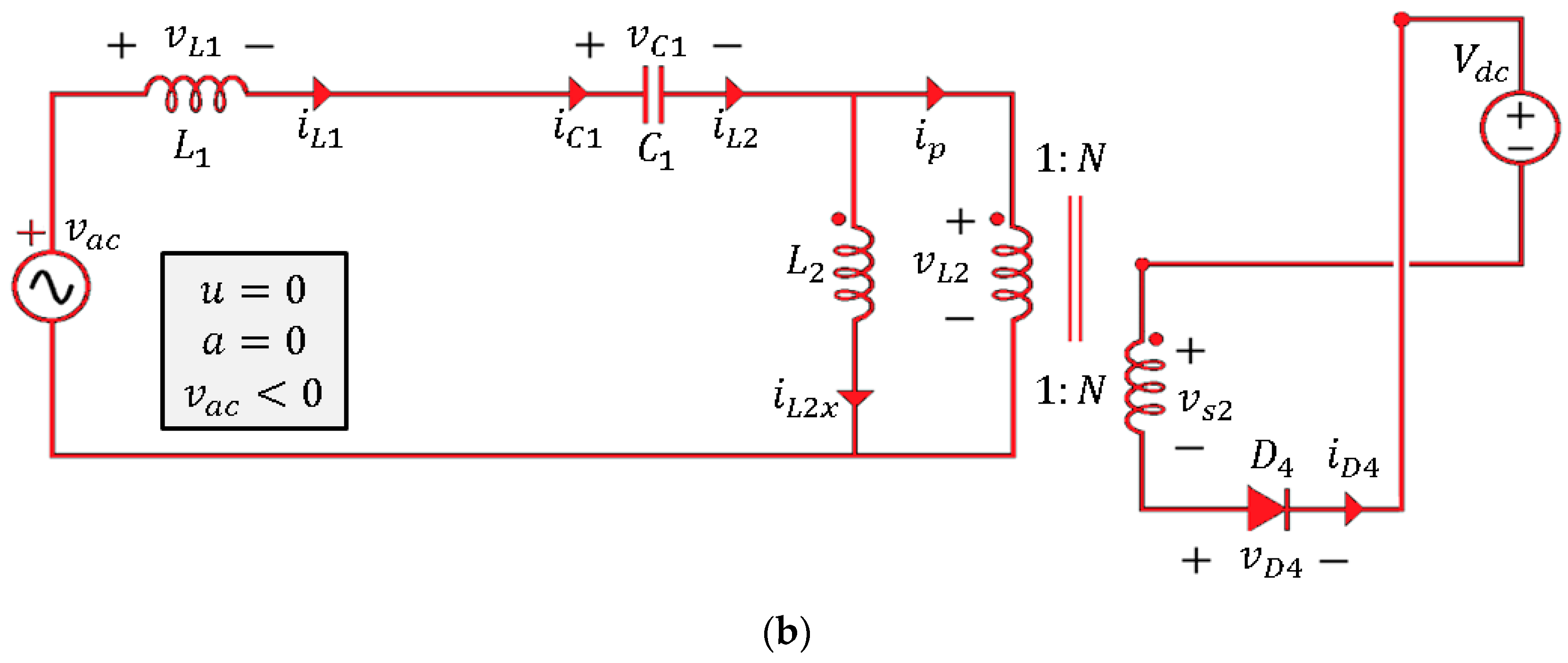
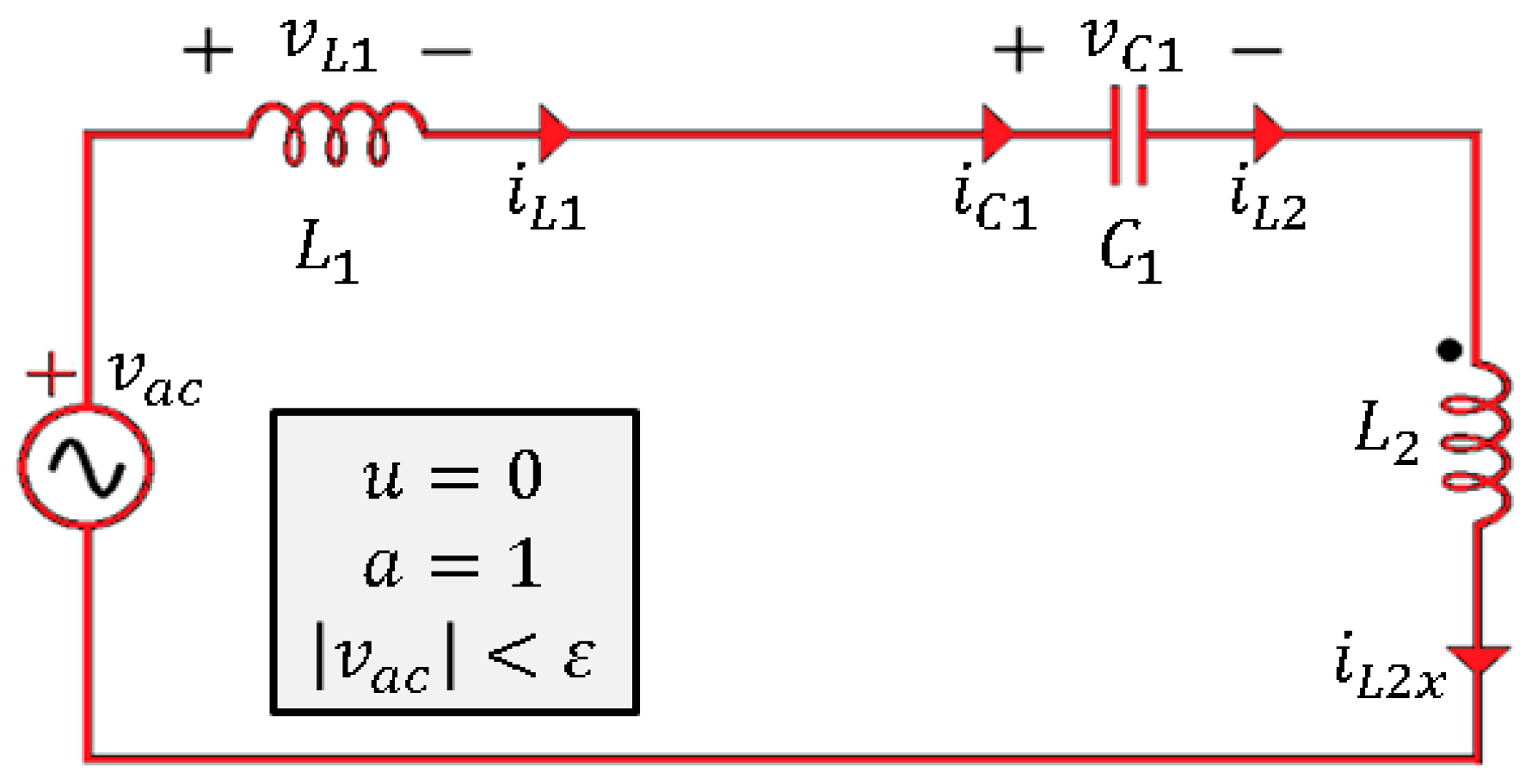
Moreover, the analysis carried out in the paper tackled—for the first time—the behavior of the isolated SEPIC circuit at zero crossing points. This additional mode cannot be considered as a trivial finding, because it differs from the known behavior of the conventional SEPIC topology used in DC–DC conversion. Nonetheless, in spite of the existence of this additional mode, the proposed sliding mode controller results to be immune to it because, after a brief dwell time in that mode, the sliding surface is quickly attained.
Our future work contemplates the study of the converter control when the coupled inductor operates in discontinuous conduction mode. This would introduce a substantial theoretical difference for the sliding motion, but it could result practically in important advantages in both the whole performance and converter power density.

Author Contributions

Conceptualization, O.L.-S., G.G., and L.M.-S.; Formal analysis, O.L.-S., G.G., and L.M.-S.; Funding acquisition, O.L.-S. and L.M.-S.; Investigation, O.L.-S., G.G., L.M.-S., and A.J.C.-C.; Methodology, O.L.-S., G.G., and L.M.-S.; Project administration, O.L.-S.; Validation, O.L.-S. and A.J.C.-C.; Writing—original draft, O.L.-S.; Writing—review & editing, O.L.-S., G.G., and L.M.-S.

Funding

This research was developed with the partial support of Colciencias under contract 018-2016, the Gobernación del Tolima under Convenio de cooperación 1026-2013, the Universidad de Ibagué under project 16-435-SEM, and the Spanish Agencia Estatal de Investigación under grants DPI2015-67292-R (AEI/FEDER, UE) and DPI2016-80491-R (AEI/FEDER, UE).

Conflicts of Interest

The authors declare no conflict of interest.

Nomenclature

i L 1 Current through the inductor L 1 .
i L 2 Current through the inductor L 2 .
i L 2 x Current through the magnetizing inductance of L 2 .
I m Amplitude of the sinusoidal current reference i r e f .
I d c Average current through the load voltage source V d c .
i r e f Reference of the current control loop.
i p Input current in the primary winding of L 2 .
i C 1 Current through the intermediate capacitor.
i D 3 Current through the diode D 3 .
i D 4 Current through the diode D 4 .
v a c AC input voltage.
v L 1 Voltage across the inductor L 1 .
v L 2 Voltage across the inductor L 2 .
v C 1 Voltage across the intermediate capacitor.
V d c LVDC bus voltage.
V m Amplitude of the sinusoidal input voltage v a c .
v D 3 Voltage across the diode D 3 .
v D 4 Voltage across the diode D 4 .
v s 1 Voltage across the secondary winding 1 of L 2 .
v s 2 Voltage across the secondary winding 2 of L 2 .
L 1 Input inductance.
L 2 Coupled inductance.
C 1 Intermediate capacitance.
S 1 Switch configuring the current path with D 2 .
S 2 Switch configuring the current path with D 1 .
N Turns ratio of the coupled inductor L 2 .
n 1 Number of turns of the primary winding of L 2 .
n 2 Number of turns of the secondary winding 1 of L 2 .
n 3 Number of turns of the secondary winding 2 of L 2 .
D 2 Diode configuring the current path with S 2 .
D 2 Diode configuring the current path with S 1 .
D 3 Diode connected to the secondary winding 1.
D 4 Diode connected to the secondary winding 2.
ε Time interval in which the sliding surface is attained after a zero crossing.
a Variable modelling the special case of zero crossing when it takes a value equal to one.
u Discrete control signal.
S ( x ) Sliding surface.
K Voltage value defined to simplify Expression (19).
K V I Constant value assigned to v a c to verify the existence of sliding modes.
K C I Constant value assigned to i L 1 to verify the existence of sliding modes.
u e q Equivalent control.
f Grid frequency.
ω Grid angular frequency.
ω a Resonance frequency of the series LC circuit that results when a = 1 .
δ Value defining the limits of the hysteresis band.
m Exponent defining the frequency 2 m f of the high-frequency signal of a digital PLL.

Appendix A

By replacing K in expression (21), the following is obtained:
i p = { V m K [ V m C 1 ω 2 sin 2 ω t I m sin 2 2 ω t ]    f o r   0 ω t < π V m K [ V m C 1 ω 2 sin 2 ω t I m sin 2 2 ω t ]    f o r   π ω t < 2 π .
Then, Expression (22) can be rewritten as follows:
i D 3 = { V m K [ V m C 1 ω 2 sin 2 ω t I m sin 2 2 ω t ] f o r   0 ω t < π        0          f o r   π ω t < 2 π .
By replacing (A2), Expression (24) becomes the following:
I d c = 1 π 0 π i D 3 d ω t = 1 π [ V m 2 C 1 ω 4 V d c 0 π sin 2 ω t d ω t + I m V m π 2 V d c I m V m 8 V d c 0 π cos 4 ω t d ω t ] , I d c = 1 π [ V m 2 C 1 ω 4 V d c cos 2 ω t | π 0 + I m V m π 2 V d c I m V m 8 V d c sin 4 ω t | π 0 ] , I d c = I m V m 2 V d c .

References

  1. Garcia, O.; Cobos, J.A.; Prieto, R.; Uceda, J. Single phase power factor correction: A survey. IEEE Trans. Power Electron. 2003, 18, 749–755. [Google Scholar] [CrossRef]
  2. Sekar, A.; Raghavan, D. Implementation of Single Phase Soft Switched PFC Converter for Plug-in-Hybrid Electric Vehicles. Energies 2015, 8, 13096–13111. [Google Scholar] [CrossRef] [Green Version]
  3. Feng, W.; Yutao, L. Modelling of a Power Converter with Multiple Operating Modes. World Electr. Veh. J. 2018, 9, 7–34. [Google Scholar] [CrossRef]
  4. Cheng, C.-A.; Chang, C.-H.; Cheng, H.-L.; Tseng, C.-H.; Chung, T.-Y. A Single-Stage High-Power-Factor Light-Emitting Diode (LED) Driver with Coupled Inductors for Streetlight Applications. Appl. Sci. 2017, 7, 167. [Google Scholar] [CrossRef]
  5. Tseng, S.-Y.; Huang, P.-J.; Wu, D.-H. Power Factor Corrector with Bridgeless Flyback Converter for DC Loads Applications. Energies 2018, 11, 3096. [Google Scholar] [CrossRef]
  6. Han, J.; Oh, Y.-S.; Gwon, G.-H.; Kim, D.-U.; Noh, C.-H.; Jung, T.-H.; Lee, S.-J.; Kim, C.-H. Modeling and Analysis of a Low-Voltage DC Distribution System. Resources 2015, 4, 713–735. [Google Scholar] [CrossRef] [Green Version]
  7. Rodriguez-Diaz, E.; Chen, F.; Vasquez, J.C.; Guerrero, J.M.; Burgos, R.; Boroyevich, D. Voltage-Level Selection of Future Two-Level LVDC Distribution Grids: A Compromise Between Grid Compatibiliy, Safety, and Efficiency. IEEE Electrif. Mag. 2016, 4, 20–28. [Google Scholar] [CrossRef]
  8. Barros, J.; de Apráiz, M.; Diego, R.I. Power Quality in DC Distribution Networks. Energies 2019, 12, 848. [Google Scholar] [CrossRef]
  9. Dragicevic, T.; Vasquez, J.C.; Guerrero, J.M.; Skrlec, D. Advanced LVDC Electrical Power Architectures and Microgrids: A step toward a new generation of power distribution networks. IEEE Electrif. Mag. 2014, 2, 54–65. [Google Scholar] [CrossRef]
  10. Guerrero, J.M.; Loh, P.C.; Lee, T.L.; Chandorkar, M. Advanced Control Architectures for Intelligent Microgrids—Part II: Power Quality, Energy Storage, and AC/DC Microgrids. IEEE Trans. Ind. Electron. 2012, 60, 1263–1270. [Google Scholar] [CrossRef]
  11. Liu, J.; Liu, Y.; Zhuang, Y.; Wang, C. Analysis to Input Current Zero Crossing Distortion of Bridgeless Rectifier Operating under Different Power Factors. Energies 2018, 11, 2447. [Google Scholar] [CrossRef]
  12. IEC. Limits for Harmonic Current Emissions (Equipment Input Current ≤ 16 A per Phase), EMC Part 3-2, IEC 61000-3-2, 3rd ed.; International Electrotechnical Commission: Geneva, Switzerland, 2005. [Google Scholar]
  13. Lin, X.; Wang, F.; Ho-Ching Iu, H. A New Bridgeless High Step-up Voltage Gain PFC Converter with Reduced Conduction Losses and Low Voltage Stress. Energies 2018, 11, 2640. [Google Scholar] [CrossRef]
  14. Ismail, E.H. Bridgeless SEPIC Rectifier with Unity Power Factor and Reduced Conduction Losses. IEEE Trans. Ind. Electron. 2009, 56, 1147–1157. [Google Scholar] [CrossRef]
  15. Sabzali, A.J.; Ismail, E.H.; Al-Saffar, M.A.; Fardoun, A.A. New Bridgeless DCM SEPIC and Cûk PFC Rectifiers with Low Conduction and Switching Losses. IEEE Trans. Ind. Appl. 2011, 47, 873–881. [Google Scholar] [CrossRef]
  16. Al Gabri, A.M.; Fardoun, A.A.; Ismail, E.H. Bridgeless PFC-Modified SEPIC Rectifier with Extended Gain for Universal Input Voltage Applications. IEEE Trans. Power Electron. 2015, 30, 4272–4282. [Google Scholar] [CrossRef]
  17. de Melo, P.F.; Gules, R.; Romaneli, E.F.R.; Annunziato, R.C. A Modified SEPIC Converter for High-Power-Factor Rectifier and Universal Input Voltage Applications. IEEE Trans. Power Electron. 2010, 25, 310–321. [Google Scholar] [CrossRef]
  18. Badin, A.A.; Barbi, I. Unity Power Factor Isolated Three-Phase Rectifier with Two Single-Phase Buck Rectifiers Based on the Scott Transformer. IEEE Trans. Power Electron. 2011, 26, 2688–2696. [Google Scholar] [CrossRef]
  19. Badin, A.A.; Barbi, I. Unity Power Factor Isolated Three-Phase Rectifier with Split DC-Bus Based on the Scott Transformer. IEEE Trans. Power Electron. 2008, 23, 1278–1287. [Google Scholar] [CrossRef]
  20. Bist, V.; Singh, B. A Unity Power Factor Bridgeless Isolated Cûk Converter-Fed Brushless DC Motor Drive. IEEE Trans. Ind. Electron. 2015, 62, 4118–4129. [Google Scholar] [CrossRef]
  21. Shi, C.; Khaligh, A.; Wang, H. Interleaved SEPIC Power Factor Preregulator Using Coupled Inductors in Discontinuous Conduction Mode with Wide Output Voltage. IEEE Trans. Ind. Appl. 2016, 52, 3461–3471. [Google Scholar] [CrossRef]
  22. Chen, Y.; Mo, S. A bridgeless active-clamp power factor correction isolated SEPIC converter with mixed DCM/CCM operation. In Proceedings of the 1st International Future Energy Electronics Conference (IFEEC), Tainan, Taiwan, 3–6 November 2013; pp. 1–6. [Google Scholar]
  23. Tibola, G.; Barbi, I. Isolated Three-Phase High Power Factor Rectifier Based on the SEPIC Converter Operating in Discontinuous Conduction Mode. IEEE Trans. Power Electron. 2013, 28, 4962–4969. [Google Scholar] [CrossRef]
  24. Hou, D.; Zhang, Q.; Liu, X. An Isolated Bridgeless Power Factor Correction Rectifier Based on SEPIC Topology. Inf. Techn. J. 2011, 10, 2336–2342. [Google Scholar] [CrossRef] [Green Version]
  25. Tanitteerapan, T.; Mori, S. Simplified input current waveshaping technique by using inductor voltage sensing for high power factor isolated SEPIC, Cûk and flyback rectifiers. In Proceedings of the Seventeenth Annual IEEE Applied Power Electronics Conference and Exposition (APEC.), Dallas, TX, USA, 10–14 March 2002; pp. 1208–1214. [Google Scholar]
  26. Tanitteerapan, T. Analysis of power factor correction isolated SEPIC rectifiers using inductor detection technique. In Proceedings of the 47th Midwest Symposium on Circuits and Systems, Hiroshima, Japan, 25–28 July 2004. [Google Scholar]
  27. Kim, J.; Han, S.; Cho, W.; Cho, Y.; Koh, H. Design and Analysis of a Repetitive Current Controller for a Single-Phase Bridgeless SEPIC PFC Converter. Energies 2019, 12, 131. [Google Scholar] [CrossRef]
  28. Rosa, A.H.R.; de Souza, T.M.; Morais, L.M.F.; Seleme, S.I. Adaptive and Nonlinear Control Techniques Applied to SEPIC Converter in DC-DC, PFC, CCM and DCM Modes Using HIL Simulation. Energies 2018, 11, 602. [Google Scholar] [CrossRef]
  29. Shieh, H.-J.; Chen, Y.-Z. A Sliding Surface-Regulated Current-Mode Pulse-Width Modulation Controller for a Digital Signal Processor-Based Single Ended Primary Inductor Converter-Type Power Factor Correction Rectifier. Energies 2017, 10, 1175. [Google Scholar] [CrossRef]
  30. Singer, S.; Erickson, R.W. Canonical Modeling of Power Processing Circuits Based on the POPI Concept. IEEE Trans. Power Electron. 1992, 7, 37–43. [Google Scholar] [CrossRef]
  31. Marcos-Pastor, A.; Vidal-Idiarte, E.; Cid-Pastor, A.; Martínez-Salamero, L. Loss-Free Resistor-Based Power Factor Correction Using a Semi-Bridgeless Boost Rectifier in Sliding-Mode Control. IEEE Trans. Power Electron. 2015, 30, 5842–5853. [Google Scholar] [CrossRef]
  32. Flores-Bahamonde, F.; Valderrama-Blavi, H.; Martínez-Salamero, L.; Maixé-Altés, J.; García, G. Control of a three-phase AC/DC Vienna converter based on the sliding mode loss-free resistor approach. IET Power Electron. 2014, 7, 1073–1082. [Google Scholar] [CrossRef]
  33. Lopez-Santos, O.; Garcia, G.; Avila-Martinez, J.C.; Gonzalez-Morales, D.F.; Toro-Zuluaga, C. A simple digital sinusoidal reference generator for grid-synchronized power electronics applications. In Proceedings of the IEEE Workshop on Power Electronics and Power Quality Applications (PEPQA), Bogota, Colombia, 2–4 June 2015. [Google Scholar]
  34. Jin, C.; Wang, P.; Xiao, J.; Tang, Y.; Choo, F.H. Implementation of hierarchical control in DC microgrids. IEEE Trans. Ind. Electron. 2014, 61, 4032–4042. [Google Scholar] [CrossRef]
  35. Erickson, R.W.; Maksimovic, D. Fundamentals of Power Electronics, 2nd ed.; Kluwer: Norwell, MA, USA, 2001. [Google Scholar]
  36. Flores-Bahamonde, F.; Valderrama-Blavi, H.; Bosque –Moncusi, J.M.; Garcia, G.; Martinez-Salamero, L. Using the Sliding-Mode Control Approach for Analysis and Design of the Boost Inverter. IET Power Electron. 2016, 9, 1625–1634. [Google Scholar] [CrossRef]
  37. Lopez-Santos, O.; Tilaguy-Lezama, S.; Garcia, G. Adaptive Sampling Frequency Synchronized Reference Generator for Grid Connected Power Converters. Commun. Comput. Inf. Sci. 2018, 915, 573–587. [Google Scholar]
Figure 1. Circuit diagram of the isolated single ended primary inductor converter (SEPIC) rectifier.
Energies 12 03463 g001
Figure 2. Circuit configurations of the isolated SEPIC rectifier: positive half-cycle.
Energies 12 03463 g002
Figure 3. Circuit configurations of the isolated SEPIC rectifier: negative half-cycle.
Energies 12 03463 g003aEnergies 12 03463 g003b
Figure 4. Configuration of the isolated SEPIC rectifier during the zero crossing of the AC input.
Energies 12 03463 g004
Figure 5. Simulated waveforms of v C 1 , u , i L 1 , i L 2 , i L 2 x , i D 3 , and i D 4 during a cycle of the AC input: (a) one-cycle waveforms; (b) zoom at positive peak of v a c ; and (c) zoom at negative peak of v a c .
Energies 12 03463 g005
Figure 6. Simulated waveform of the equivalent control u e q and u e q = 1 u e q during a cycle of v a c .
Energies 12 03463 g006
Figure 7. Detail of i L 1 waveform at a zero crossing for condition 1: (a) using an ideal comparator and (b) using a hysteresis comparator.
Energies 12 03463 g007
Figure 8. Detail of i L 1 waveform at a zero crossing for condition 2: (a) using an ideal comparator and (b) using a hysteresis comparator.
Energies 12 03463 g008
Figure 9. Control diagram of the isolated SEPIC high power factor (HPF) rectifier.
Energies 12 03463 g009
Figure 10. Converter prototype.
Energies 12 03463 g010
Figure 11. Experimental setup used in laboratory experiments.
Energies 12 03463 g011
Figure 12. Current and voltage waveforms at the AC side of the converter during a 31 W test: (a) simulated results and (b) experimental results. Scales: 0.5 A/div and 100 V/div.
Energies 12 03463 g012
Figure 13. Current and voltage waveforms at the AC side of the converter during a 95 W test: (a) simulated results and (b) experimental results. Scales: 1 A/div and 100 V/div.
Energies 12 03463 g013
Figure 14. Power quality measurements: (a) test at 25% of the nominal power and (b) test at 80% of the nominal power.
Energies 12 03463 g014
Figure 15. Oscilloscope captures during 400 ms showing dynamic behavior of the converter for changes from 0.25 A to 0.75 A, and vice versa. At the top, a 40 ms zoom details three cycles of the current waveform for each current level. At the bottom, a 200 µs zoom details the high frequency components.
Energies 12 03463 g015
Table 1. Converter dynamics during a positive half-cycle.
Differential Equations On-State ( u = 1 ) Differential Equations Off-State ( u = 0 )
L 1 d i L 1 d t = v a c L 1 d i L 1 d t = v a c v C 1 V d c N
L 2 d i L 2 x d t = v C 1 L 2 d i L 2 x d t = V d c N
C 1 d v C 1 d t = i L 2 x C 1 d v C 1 d t = i L 1
i D 3 = i D 4 = 0 i D 3 = 0 ; i D 4 > 0
v S 1 = v S 2 = N v C 1 v S 1 = V d c
Table 2. Converter dynamics during a negative half-cycle.
Differential Equations On-State ( u = 1 ) Differential Equations Off-State ( u = 0 )
L 1 d i L 1 d t = v a c L 1 d i L 1 d t = v a c v C 1 V d c N
L 2 d i L 2 x d t = v C 1 L 2 d i L 2 x d t = V d c N
C 1 d v C 1 d t = i L 2 x C 1 d v C 1 d t = i L 1
i D 3 = i D 4 = 0 i D 3 > 0 ; i D 4 = 0
v S 1 = v S 2 = N v C 1 v S 2 = V d c
Table 3. Converter dynamics during zero crossings of the alternative current (AC) input signal.
Differential Equations ( u = 0 )
( L 1 + L 2 ) d i L 1 d t = v a c v C 1
( L 1 + L 2 ) d i L 2 x d t = v a c v C 1
C 1 d v C 1 d t = i L 2 x = i L 1
i D 3 = i D 4 = 0
v S 1 = v S 2 = 0
Table 4. Specification, parameters, and main components of the laboratory prototype.
ParameterSymbolValueUnits
Nominal input voltage V g 120V
Nominal power P 100W
Input frequency f g 60Hz
DC voltage V d c 400VDC
SuperMesh Technology N-Channel MOSFET S 1 and S 2 950V
STD6N95K59A
MOSFET on-resistance R d s o n 1.25
SiC Schottky diodes D 1 , D 2 , D 3 and D 4 1700V
GP2D005A170B5A
Input inductor (Bourns 1140-222-RC) L 1 2mH
Coupled inductor (TDK E 55/28/21 Core) L 2 1mH
Primary winding (20 AWG) N 1 36turns
Secondary windings (24 AWG) N 2 , N 3 78turns
Intermediate capacitor (EPCOS Z115056959) C 1 1µF
Table 5. Equipment used in the experimental setup.
EquipmentModelCapacity
Programmable DC loadIT8512B+600 V/300 W
OscilloscopeTDS2024C50 MHz
Digital Multimeter34401A600 V
Power source for control circuitsGPC-3030D30 V/3 A
Power quality analyzerFLUKE 43B600 V
Table 6. Frequency content of the input voltage (total harmonic distortion (THD) = 3.5%).
Frequency (Hz)Amplitude (V)Phase (°)
60 120 2 0
300 3.4 2 −144
420 1.4 2 20

