Abstract
A comparative analysis of the dynamic features of a step-up microinverter based on the cascade connection of two synchronized boost stages and a full-bridge is presented in this work. In the conventional approach the output of the cascaded boost converter is a 350–400 DC voltage that supplies the full-bridge that makes the DC-AC conversion. Differently from the classical approach, in this work, the cascaded boost converter delivers a sinusoidal rectified voltage of 230 Vrms to the full-bridge converter that operates as unfolding stage. This stage changes the voltage sign of one of every two periods of the rectified sinusoidal signal providing the final output AC waveform. In contrast to a classical full-bridge inverter, the unfolding stage lacks output filter, and has zero order dynamics. Thus, the approach presented here implies a second order dynamics reduction that will be increased applying sliding motions to control the system. After introducing the inverter circuit, two sliding control alternatives, input current mode and pseudo-oscillating mode, are presented. Both alternatives are analyzed, simulated, and verified experimentally. Furthermore, detailed description of the microinverter power stage and control circuits are also given.
1. Introduction
Practical applications for microinverters are gradually increasing, from autonomous systems based on renewable energies, to supply small electrical appliances in embedded systems. Essentially, a microinverter is a low-power converter employed to obtain a sinusoidal AC waveform from a low DC voltage value, such as the one provided by a car battery, a photovoltaic module, or a fuel cell stack. The power rating of a microinverter is usually below 200 W, and the output voltage and frequency are those of the electrical grid.
Microinverters can be classified into two groups. The first group comprises all converter circuits behaving as an AC current source [1,2]. These are typically used in PV grid-tie applications, such as in the AC-module concept [2]. The second group of microinverter topologies operate as AC voltage sources. Consequently, these circuits are particularly suited for stand-alone.
Normally, a microinverter has two stages, see Figure 1. The first-stage is usually a step-up converter type, and the second stage is commonly a full-bridge inverter. Galvanic isolation [3] can be incorporated either in the first stage, or in the second one.
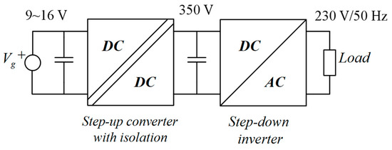
Figure 1.
General diagram of the conventional microinverter configuration.
Many different two-stage microinverter topologies have been proposed in order to provide a large AC voltage (230 Vrms, 50 Hz) from a low DC supply in the range of 9 to 16 V [3,4,5].
A common approach consists of boosting the DC voltage above the required AC peak voltage in the first stage, whereas the second one realizes the inverting function (Figure 1). Sometimes, a high-frequency isolation transformer is used in the DC-DC stage to achieve a large conversion ratio avoiding extreme duty ratios. This can be achieved by using, for example, two interleaved flyback converters [5,6,7]. Nevertheless, if galvanic isolation is not required, those approaches are far from being optimal in power density, weight, size, and cost. Figure 2 depicts diverse converter static gains.
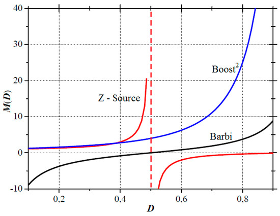
Figure 2.
Ideal static transfer function M(D) of different converters.
Since there is growing interest in developing transformerless alternatives [3], several single-stage approaches have been proposed. Among the most reported configurations are the boost inverter (also named Barbi) [8,9,10], shown in Figure 3a, and the Z-source inverter [8], in Figure 3b. Although these last approaches avoid the use of a transformer, they exhibit a high nonlinear behavior and offer a very limited gain conversion ratio (typically below 10), and a poor efficiency [5,6,7,8,9,10,11,12], resulting in non-competitive solutions. This is especially important, in the Z-source inverter, where the shoot-through states management complicates the converter control, and the high-stress of the switching devices reduces the efficiency.
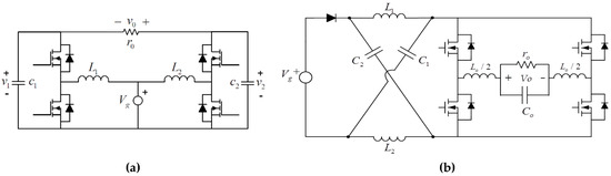
Figure 3.
Single-stage transformerless inverters with small voltage gain: (a) Boost inverter (Barbi), and (b) Z-source single-phase inverter.
Two-stage microinverters, based on the combination of a step-up DC-DC converter and a step-down DC-AC inverter can avoid the use of a transformer and achieve a large conversion ratio at the same time [5]. In this context, topologies derived from the quadratic boost converter [12,13,14] are advantageous. Quadratic boost converters can provide larger gain conversion ratios at lower duty ratios, exceeding the voltage gain capabilities of the Z-source and Barbi converters, as shown in Figure 3. The efficiency analysis of four quadratic boost topologies presented in [4,13] shows that the quadratic voltage gain topology with the highest efficiency is the cascade connection of two boost converters in synchronous operation.
To summarize, this work employs the same quadratic boost topology under an advantageous operational mode in which the first stage of the microinverter is responsible for generating the AC waveform. In order to regulate the converter, two control methods providing robustness and tight performances are proposed and compared.
The remainder of this paper is structured as follows. In Section 2, the proposed operational mode is presented and compared with the conventional approach, showing their advantages and drawbacks. In Section 3, the dynamics of the proposed operational mode are analyzed. Next, in Section 4 and Section 5, two sliding-mode control methods are proposed to regulate the converter. The first controller, based on the control of the input current of the microinverter, is introduced in Section 4. The second controller, which exhibits a self-oscillating behavior, is proposed in Section 5. Section 6 shows the inverter power stage and the control circuits for the two proposed controllers. The experimental results verifying the proposed operational mode and comparing the results of the two controllers are given in Section 7. Finally, Section 8 shows the work conclusions and some research guidelines.
2. Comparison of Microinverter Operation Strategies
Figure 4 depicts the two different operation strategies. The conventional approach depicted in Figure 4a is named ”slow-fast” approach in this work. The proposed operational mode, shown in Figure 4b, is named “fast-slow”.
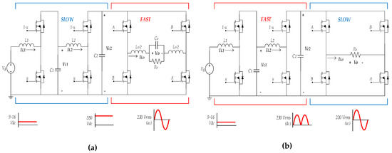
Figure 4.
Strategies to perform a step-up inverter based on a two cascaded-boost converter: (a) conventional approach (slow-fast), (b) proposed approach (fast-slow).
In the “slow-fast” operation, the first stage provides a large DC intermediate voltage Vc2 in the range of 350–400 V whereas the full-bridge inverter realizes the DC-AC conversion. The output voltage is obtained with a bipolar or unipolar sinusoidal PWM modulation (SPWM). Although at equal switching frequency the unipolar modulation exhibits lower switching losses than the bipolar one, the unipolar modulation requires a more complicated switching logic.
Oppositely, in the “fast-slow” approach, the first stage converter provides a rectified sinusoidal voltage of amplitude and the unfolding stage makes the sign inversion. In this case, as the full-bridge is switching at 50 Hz and the switching losses are negligible.
The only drawback of this strategy is that the quadratic boost minimum output voltage is Vg instead of zero, causing a zero-cross distortion problem in the inverter output voltage that is addressed in Section 6.
According to Figure 4, no matter what the selected strategy is, “slow-fast” or “fast-slow”, the first stage is always a quadratic boost converter, and consequently, a fourth order plant. Nevertheless, in the “slow-fast” strategy, the second stage is a buck inverter, and has a second order dynamics; whereas in the “fast-slow” approach, the full-bridge is an unfolding stage, lacks an output filter, and has zero-order dynamics. Figure 5 compares both microinverter operation strategies.
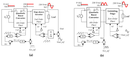
Figure 5.
Common and proposed approaches with PWM control: (a) common case (slow-fast): 6th order plant, 9th -10th order system depending on inverter controller; (b) fast-slow strategy: 4th order plant, 6th order system.
Assuming PWM control, Figure 5 shows the control loops required for each approach. Both strategies require a two-loop controller to regulate the first stage output voltage according to a given voltage reference (constant in case of Figure 5a, variable in case of Figure 5b). The main dynamical difference comes from the full-bridge stage operation. In the conventional approach the full bridge is a buck inverter and requires a PR (proportional resonant) or PI (proportional integral) controller to track a sinusoidal reference to obtain a sinusoidal output voltage. Although PR is normally preferred because it can totally cancel the tracking error, differently from the PI; the PR is a second order controller whereas the PI has a single pole at the origin. In the fast-slow approach, the full-bridge is used to alternately change the output voltage sign, and only a comparator (a zero dynamics controller) is required.
The pole position of the quadratic boost small-signal output-to-control transfer function depends on the converter duty ratio. Whereas in the conventional approach the first stage output voltage VC2 is constant (350 V), and the duty ratio only depends on the input voltage variations, in the “fast-slow” strategy the poles variability is enhanced because vC2(t) is ranging from Vg to the output voltage peak . This fact could complicate the control design and constitutes an additional issue that justifies the use of sliding mode control.
Among Sliding Mode Control (SMC) advantages, the most known are the following: simplicity of implementation, inherent robustness against perturbations and parametric variations, and dynamic order reduction. As the microinverter has two stages, a control surface per converter-stage, this means two surfaces, could be considered.
Applying sliding motions implies a system-dynamics order reduction per surface. In the conventional “slow-fast” approach the PWM-controlled 6th order plant, when sliding motions are applied, becomes a 4th order plant. Thus, the quadratic boost dynamics is reduced to a third-order plant, and then, the second-order full-bridge inverter stage becomes a first-order plant.
Conversely, in the “fast-slow” strategy, as the second microinverter stage has no dynamics, no control surface is required. As a result, the whole “fast-slow” microinverter plant becomes a third-order system, one order less than in the conventional “slow-fast” approach.
In addition, if sliding motions are applied in the “fast-slow” approach, to assure that the quadratic boost output tracks the reference voltage, a PI regulator is required, obtaining finally a 4th order system. Finally, it is worth mentioning that the order of the system would be much higher if regular PWM regulators would be used in these plants. With the “fast-slow” approach, the system would exhibit 6th order dynamics. With the “slow-fast” operation, the order would even be higher, adding up to 9th order.
In this work, two different sliding surfaces are applied to a quadratic-boost “fast-slow” microinverter operating with the “fast-slow” strategy. The first proposed controller (Figure 6a) is based on input current regulation [12], whereas the second proposed controller (Figure 6b) is based on a self-oscillating behavior [15,16]. After steady state analysis in Section 3, the input current surface is analyzed in Section 4, and the self-oscillating surface in Section 5.
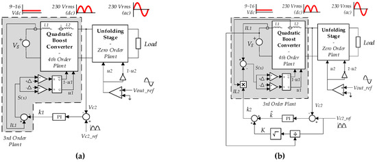
Figure 6.
Output voltage regulation. Proposed sliding surfaces: (a) using the microinverter input current , (b) inducing a self-oscillating motion .
3. “Fast-Slow” Microinverter Analysis
Figure 4 shows the schematic of the proposed “fast-slow” step-up inverter based on the cascade connection of two boost circuits. The goal is to achieve a sinusoidal voltage signal, v0(t), of a given RMS value and frequency from a low DC input voltage, vg(t). To do that, the voltage at the output of the quadratic boost stage, vc2(t), must be kept at a given reference value vref(t) despite disturbances, see Equation (1).
Only the quadratic boost stage is analyzed due to the zero dynamics of the unfolding stage. The fast stage is a fourth-order variable structure system with its two commutation cells in synchronous operation. Continuous conduction mode (CCM) operation was assumed. As shown in Figure 7, this converter has two equivalent circuit configurations for CCM operation during a switching period.
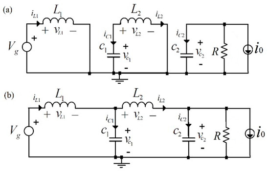
Figure 7.
Cascade-boost converter topologies: (a) ON, and (b) OFF.
In the equation set, current source i0(t) models load disturbances, R models the converter nominal load, and L1, L2, C1, and C2, stand for the inductances and capacitances values, respectively. Thus, the dynamic expressions in state-space at each position of the switch are characterized as,
where Ai and Bi (i∈{1, 2}) are the state matrices and the input vector respectively, and for each subinterval (Ton and Toff), and where x(t) = [iL1, iL2, vC1, vC2]T is the state vector, which groups the inductor currents and capacitor voltages.
Thus, Equation (2) can be compacted into a single bilinear form, see Equation (3):
where the discrete control variable stands for the gate signal of the low-side controlled switches of the two-cascade-boost circuits, which force the commutation between Ton and Toff.
In summary, the converter switching dynamics can be written as
Replacing the control variable u(t) in Equation (4) by its averaged value, the duty cycle D(t), the ideal quadratic-boost converter quasi-static gain M[D(t)], operating in CCM, can be obtained using Equation (5). The corresponding permanent-regime averaged state vector x(t) = [iL1(t), iL2(t), vC1(t), vC2(t)] is given in Equation (6). Realize that switching frequency is at least three orders of magnitude higher than the variation frequency of the sinusoidal averaged state variables.
Finally, to obtain a regulated output voltage, rejecting input voltage perturbations and load variations, a two-loop system is required. The outer-loop regulates the output voltage with a PI controller. For the inner-loop two sliding mode surfaces are proposed: an input current surface (Equation (7)) analyzed in Section 4, and a self-oscillating one (Equation (8)) studied in Section 5.
4. Microinverter Control with Input Current Approach
In this mode of operation, the control law forces the input current,
, to track a signal of the form k(t) = Ksin2(ωot). Realize that this fact is in perfect agreement with the state vector in permanent regime (Equation (6)), the sliding mode control-law described in Equation (7), and the PoPi behavior of any converter. Figure 8 depicts the block diagram of input current control strategy.
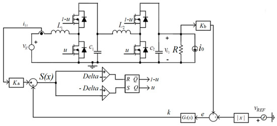
Figure 8.
Input current control strategy.
The outer-loop establishes the reference of the inner loop by means of a PI compensator GC(s) processing the voltage error e(t). Figure 8 illustrates the hysteresis-based two-loop control, where the inner current loop is defined by means of a sliding surface (Equation (7)), which drives the converter to a stable desired point.
Assuming the frequency is considerably lower than the switching frequency, i.e., the evolution of the sliding surface is much slower than the transients among states, it can be considered that the input inductor current follows its reference k1(t).
The discontinuous switching function u(t) that yields sliding motion is given in Equation (11).
Based on the sliding surface (Equation (7)) and applying the invariance conditions (S1(x,t) = 0 and dS1(x,t)/dt = 0) to the converter equation set (Equation (4)), the equivalent control (Equation (12)) is obtained. The control will exist unconditionally since vC1(t) > 0, ∀t > 0.
Now, by replacing the expression of the equivalent control (Equation (12)) in the converter equation set (Equation (4)) and considering the surface (Equation (7)), iL1(t) = k1(t), the resulting ideal sliding dynamics is obtained. As the input current iL1(t) dynamics is given by the external reference k1(t), the remaining system dynamics is reduced one order once the surface is reached.
The nonlinear behavior of the ideal sliding dynamics is depicted in Equation (13). To synthesize an appropriate controller using a small-signal model, a linearization around the equilibrium point is required. By means of a quasi-static approximation [16] the state vector x(t) evolution can be modelled as a succession of equilibrium points that evolve according the output voltage sinusoid value, that it f(θ) = |sin(θ)| = |sin(ωot)|. By nullifying the derivatives in Equation (13), the succession of equilibrium points (Equation (14)) is obtained.
Once the equilibrium points are calculated, the linearization of the ideal sliding dynamics (Equation (13)) to get a small-signal linear model around a given equilibrium point (Equation (14)) is a well-known procedure. The equation set of Equation (15) is the linearized version of Equation (13).
The corresponding coefficients of the linearized model (Equation (15)) are calculated by means of the Jacobian matrix and given in Equation (16).
Placing the coefficient values (Equation (16)) in the linearized model (Equation (15)) and taking the Laplace transform the corresponding small-signal model transfer functions are obtained. Figure 9 shows the closed-loop small-signal diagram block. The controller box GC(s) included in Figure 9 accounts for the PI integrator that closes the voltage loop.
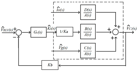
Figure 9.
Block diagram of the output voltage regulation loop.
Then, considering the PI controller transfer function is GC(s) = kP + kIn/s, the closed-loop transfer function is derived (Equation (17)), where Ka and Kb represent the input current and output voltage sensor gains, respectively. The model polynomials A(s), B(s), C(s) and D(s) are given in Equation (18). As can be deduced from Equation (18) the converter poles, zeros, and gains are found to vary along the AC output sinusoid.
4.1. Parameter Variation Analysis
To appropriately design the PI coefficients kP and kIn, it is convenient to realize a parametric study of the root-locus of the open-loop control-to-output transfer function . Two different average output powers are considered: the nominal case (100 W) and twice that power.
The main converter parameters are R = {250, 1000} Ω, Vg = 13 V, L1 = 8 μH, L2 = 800 μH, C1 = 0.5 μF, C2 = 0.8 μF, ωo = 100π rad/s, Ka = 0.2 V/A, Kb = 0.01 V/V, 2.5° < θ < 90°. Figure 10a charts the poles and zeros placement for 100 W (K1 = 16.67 A) and Figure 10b shows it for twice the power (K1 = 33.33 A).
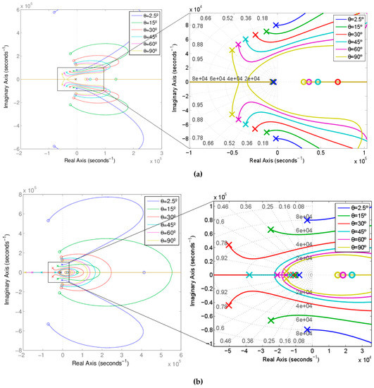
Figure 10.
Root locus of (a) for 100 W, (R = 484 Ω, K1 = 16.67 A); (b) for 200 W, (R = 242 Ω, K1 = 33.33 A)
By inspection of Figure 10a, it is clear the existence of a real dominant pole on the left half-plane for θ > 7.5°, and a pair of complex conjugate poles whose damping increases when the output voltage or the angular parameter θ increase. The dominant pole location is proportional to the mean output power. Thus, for 100 W the pole is at s = −5·103 rad/s, whereas for 200 W it is close to s = −104 rad/s.
The behavior for 100 and 200 W is similar. In both cases there are real right half-plane zeros and all the poles are in the left half-plane. Nevertheless, as depicted in Figure 10b, in the 200 W case, there is a dominant pole while θ < 60°, but for θ > 60°, the system exhibits is a second order dominance with a pair of complex conjugate poles with a damping factor close to 1.
4.2. Synthesis of the Voltage Regulation Loop
To assure at least local closed-loop stability for all operation ranges ωot = θ ∈ [0, π/2], the Routh–Hurwitz criterion is applied to the closed-loop characteristic polynomial (Equation (19)) of the voltage regulation transfer function (Equation (17)).
According to the Routh criterium, the small-signal stability of the system can be ensured if the following set of constraints is satisfied:
From the aforesaid procedure, a stable region in the kP − kIn plane can be derived. Given the nominal input voltage, output voltage, and load R, Figure 11 charts the PI controller constants to assure stability (Equation (21)) for a representative set of θ values. In the nominal case, stability is assured if kP ∈ [0, 1.23] and kIn ∈ [0, 4·105]. Equivalent plots were considered for other load and input voltage values. Finally, to enhance the transient performance, and assure stability, the following gains were selected kP = 1, and kIn = 2·104.
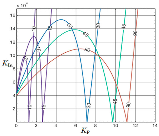
Figure 11.
Evaluation of the stability region in the kP - kIn plane, for the nominal case.
5. Microinverter Control with Self-Oscillating Approach
As in the previous case, an invariant rectified sine signal of and 100 Hz at the output of the two cascaded-boosts stage is required. Unlike in the previous input current control, the reference output voltage is achieved establishing a proportional relationship k2(t) among both inductor currents, iL1(t) and iL2(t). In this case, differently from previous works [15,16,17], k2(t) is a time-variant signal modulated by an external reference signal.
The self-oscillation approach implies that a system is self-switching, with any external reference causing the converter state changes, and the resulting output voltage gain depends only on the value of the proportionality constant. However, in this particular case, as the quadratic-boost output voltage must track a given reference voltage, in a quasi-static approximation, the proportionality constant k2(t) must also change slowly to assure that the output voltage is a sinusoidal signal. To find the required steady-state link between the two inductor currents K2(ωot), the following conditions need to be considered: (i) the converter exhibits a PoPi behavior (Vg·IL1 = VC1·IL2), and (ii) the medium voltage capacitor is the geometric mean of the input and output voltage (Equation (6)).
It is worth mentioning that load perturbations will not affect the proportionality constant K2(ωot). As a result, this control-law should assure ideal load regulation, and by means of the implicit nonlinear Vg feedforward (Equation (22)), an ideal line regulation could also be expected. Nevertheless, as converter losses exist, and intending to compensate those losses or any other perturbation, a PI controller is used, resulting in the aforesaid sliding surface (Equation (8)).
The main difference between Equations (7) and (8) is that the voltage regulation PI controller of the input current approach is in charge of computing the reference current completely by itself, whereas in the self-oscillating approach we establish the equilibrium point of the converter by means of K2(θ) (Equation (22)), and therefore the output of the PI compensator will be zero unless a disturbance arises. Furthermore, to perform an effective line regulation in Equation (8), a feedforward control loop is required to update the steady-state relationship among inductor currents (Equation (22)) effectively and rapidly.
The main interest of this control method is that it is possible to fix the output voltage through a correct selection of the transformation ratio (Equation (23)), despite output power requirements (transformer characteristic). Hence, no feedback control loop would be required if there were no conversion losses. Figure 12 depicts the control block diagram of the self-oscillating strategy.
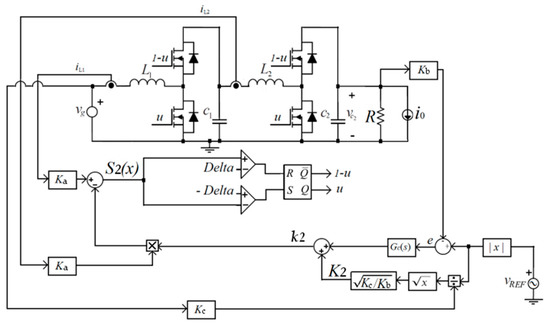
Figure 12.
Self-oscillating control strategy.
Based on the sliding surface (Equation (8)) and applying the invariance conditions in the dynamics of the converter (Equation (4)), leads to the equivalent control (Equation (23)).
Unlike in the input current control, where there is an unconditional transversality, the self-oscillating surface has a conditional transversality, and the existence of an equivalent control must be ensured through a correct design of both inductors. A possible solution for that is given in Equation (24).
From the equivalent control expression (Equation (23)), the converter equation set (Equation (4)), and the surface (Equation (8)), the resulting ideal sliding-mode dynamics of the converter (Equation (25)) can be derived.
The equilibrium point (Equation (26)) is derived by nullifying the derivatives in the nonlinear dynamics (Equation (25)). As shown in Equation (26) it has a variable transformer characteristic, with turns ratio n = VC2/Vg = K2(θ). The small signal control block diagram is shown in Figure 13.
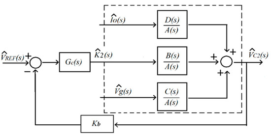
Figure 13.
Block diagram of the output voltage regulation loop.
By linearizing the ideal dynamics (Equation (25)) around the equilibrium point (Equation (26)), it is possible to obtain a small signal model (Equation (27)),
where coefficients are defined in Equation (28).
As in the previous case, the linearized dynamics (Equation (27)) allows to determine the open-loop transfer functions of the small signal model depicted in Figure 13. Note that in this case, the output of the controller is understood as the variation of the ratio among inductor currents instead of the variation of the input current reference amplitude, as in the input current surface.
The polynomials A(s), B(s), C(s), and D(s), defining the small signal model transfer functions are shown in Equation (29), and as in the previous case, the poles and zeros have also a clear dependence of K2, R, Vg, and sin(θ). The characteristic polynomial of the closed-loop transfer functions is defined in Equation (30).
5.1. Parameter Variation Analysis
Figure 14a,b depict the root locus of the open-loop control-to-output (plant) transfer function = B(s)/A(s) in the same test conditions and with the converter component parameters used in the previous case, the input current surface.
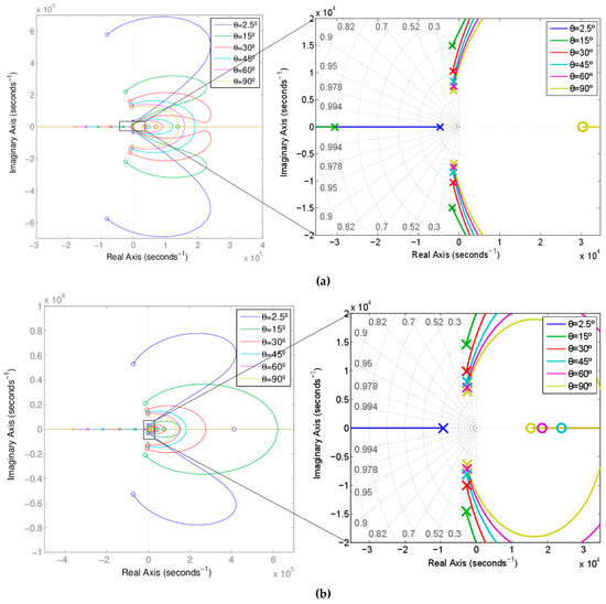
Figure 14.
Root locus of for (a) 100 W, (R = 484 Ω), (b) for 200 W, (R = 242 Ω).
The charts of Figure 14 show the existence of a pair of complex conjugate dominant poles on the left half-plane. Just as in the input current control case, the real part of the dominant complex conjugate poles is proportional to the output power. Thus, for 100 W the real part is Re[s] = −1380 rad/s and for the 200 W case Re[s] = −2640 rad/s. As in the preceding case, the damping factor ζ of the dominant poles increases with the load instantaneous power, this means when ωot = θ increases from 0° to 90°. On the contrary, in the preceding case, the damping factor could reach ζ = 1, and here the damping never exceeds 0.38, and the dynamics is more oscillatory.
Nevertheless, and this is the most important, with the first control technique, the plant of the converter could be approximated by means of a first order system whose dynamics are four times faster than in the self-oscillating approach. In addition, the proximity of the dominant complex poles to the imaginary axis in the self-oscillating approach in conjunction with the non-minimum phase behavior further complicates the design of the control loop due to the lower bandwidth.
5.2. Synthesis of the Voltage Regulation Loop
In a similar way to the previous case, the Routh–Hurwitz criterion is used to assure, at least, local stability in closed-loop. Once the Routh criterion is applied to the characteristic polynomial P(s) (Equation (30)), the corresponding stability constraints are given in Equation (31), and the kP-kIn chart is also obtained.
Similarly, as is done with the input current control surface, from the aforesaid procedure, a stable region in the kP - kIn plane can be derived. Given the nominal input voltage, output voltage, and load R, Figure 15 charts the PI controller constants to assure stability (Equation (31)) for a representative set of θ values. In the nominal case, stability is assured if kP ∈ [0, 0.72] and kIn ∈ [0, 2·103]. Equivalent plots were considered for other load and input voltage values. Finally, to enhance the transient performance, and assure stability, the following gains were selected kP = 0.5, and kIn = 103.
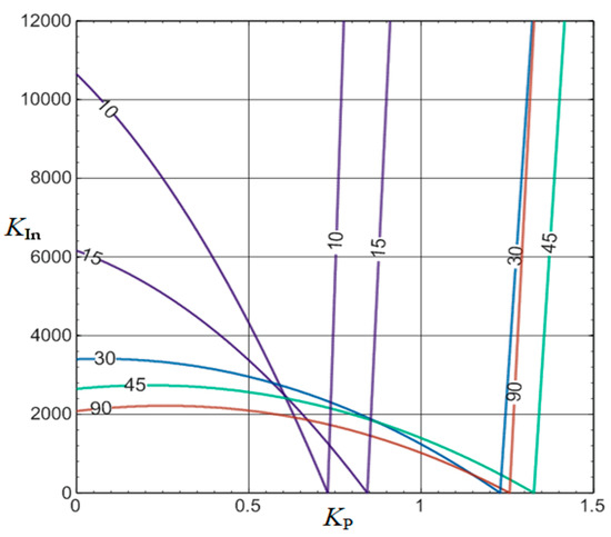
Figure 15.
Evaluation of the stability region in the KP - KIn plane for the nominal case.
6. Inverter Realization
In this section, the realization of a 100 W a “fast-slow” inverter prototype using two cascaded-boost circuits and an unfolding-stage is discussed, and the resulting power stage and control circuit schematics will be given. Nevertheless, the quadratic step-up nature of the microinverter first stage, makes the minimum output voltage of this stage equal to the input voltage Vg. Then, as this voltage cannot reach zero, the inverter output voltage changes instantaneously from Vg to −Vg and/or vice-versa each time where ωot = k·π, causing a zero-cross distortion. This is the first issue to solve.
6.1. Solving the Zero-Cross Distortion of the “Fast-Slow” Approach
The first option could be a hybrid operation of the microinverter second stage. During most of the sinusoidal cycle the full-bridge can operate as unfolding stage. However, at the vicinity of the zero-crossing instants ωot = k·π, the full-bridge output could be PWM modulated to smooth the output voltage in the zero-cross region. However, to be operative a PWM requires that a second-order low-pass output filter is required. If the filter operates the whole sinusoidal cycle, the positive effects of the “fast-slow” approach are eliminated, that is, the zero-order dynamics of the unfolding stage. If the filter only operates in the zero-cross region, the complexity of the control circuit increases.
A second solution consists of connecting the unfolding stage in differential mode to the microinverter first stage. In other words, the ground of the unfolding stage is connected to the input voltage terminal Vg. This solution is depicted in Figure 16a.
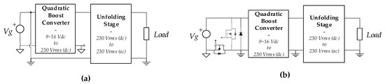
Figure 16.
Solutions for the output voltage distortion in the “fast-slow” approach: (a) Unfolding stage differential connection, and (b) introducing a Buck-switch cell.
Figure 16b depicts the chosen solution. A buck-switch stage is connected between the input source and the microinverter first stage. This buck-switch disconnects the first stage from the input source voltage some hundreds of microseconds around the zero-crossing instants ωot = k·π. During these disconnection periods, the quadratic-boost input voltage is zero, the output voltage can reach zero voltage, and the zero-cross distortion is eliminated.
6.2. Power-Stage Circuits and Implementation
The inverter was designed to deliver an output regulated voltage of 230 Vrms/50 Hz for an input voltage range from 9 to 16 V, and an output load range from 50 to 200 W. The converter component values are L1 = 8 μH, L2 = 800 μH, C1 = 0.5 μF, and C2 = 0.8 μF. Capacitor C1 is implemented with a set of 10 parallel 47 nF multilayer ceramic capacitors (MLCC) and capacitor C2 with a set of eight parallel 100 nF tantalum electrolytic type ones. Both types are characterised by a low series resistance and high voltage capability, appropriate for switching applications.
The following MOSFET transistors were selected: (a) the IRFB4110PBF (180 A, 100 V, 4 mΩ) for the Buck-switch cell, (b) the IPP110N20NA (88 A, 200 V, 9.9 mΩ) for the high-side and low-side switches of the first boost cell, (c) the SiC MOSFETs C3M0120090D (23 A, 900 V, 120 mΩ) for the second boost cell, and finally (d) for the unfolding stage switches, the SPW47N60C3 device (47 A, 650 V, 70 mΩ) was used.
Several driver ICs are used: two IR2110 are used in the quadratic boost, two IR21834 are used in the unfolding stage, and a low-side only driver MCP1407P is employed in the buck-switch stage. The free-wheeling MOSFET of the buck-switch stage is driven by a complementary bipolar transistor pair (ZTX653/ZTX753), for the free-wheeling MOSFET. Figure 17, Figure 18, Figure 19 and Figure 20 depict the power stage circuits.
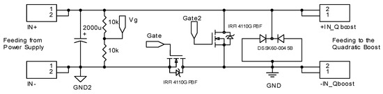
Figure 17.
Power stage circuit of the Buck-switch cell.
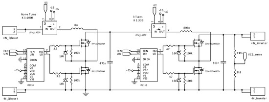
Figure 18.
Power stage circuit of the proposed Quadratic Boost.
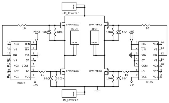
Figure 19.
Power stage circuit and drivers of the unfolding/inverter stage.
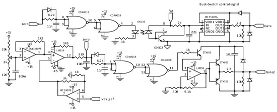
Figure 20.
Zero-crossing detection circuit and Buck-switch control drivers.
6.3. Control-Surfaces and Voltage-Loop Implementation
To implement the proposed sliding mode control surfaces, a hysteretic comparator is required. For practical reasons to be explained in Section 7, and related to the experimental results, two different type of hysteresis are available for test purposes: constant and variable. The inverter will be able to operate with any of them. The constant hysteresis width Δdc, can be adjusted in the range Δdc = [0.1,0.3]. In the variable hysteresis type Δ(t) = Δdc+Δv·|sin(θ)|, the offset Δdc and the amplitude Δv can be adjusted, where Δv = [0.1,0.5]. The hysteresis parameters have a considerable impact in the microinverter switching losses and conversion efficiency. Figure 21, Figure 22 and Figure 23 depict the control circuits.
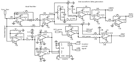
Figure 21.
Generator of ancillary signals.
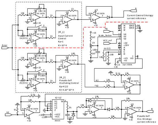
Figure 22.
Control-loop and surface generator.

Figure 23.
Sliding surface selection and hysteretic comparator.
Figure 21 depicts diverse ancillary functions. Taking a sinusoidal signal from a function generator, this circuit board generates (a) the output voltage reference signal vref(θ) = |sin(θ)| by means of an ideal rectifier, (b) the output voltage error e(t) = vref(t)-vC2(t), (c) the unfolding-stage switching signals HIN2 and LIN2, and finally (d) both hysteresis widths, the constant one and the variable.
7. Experimental Results
Figure 24 shows a photograph of the microinverter prototype and the experimental set-up. This test environment includes a Delta Elektronika SM70-45-D (3 kW, 70 V, 45 A) power supply for the power stage, a TENMA 72-10505 (90 W, 30 V, 3 A) to supply the control circuit, a Yokogawa DLM4038 (2.5 GS/s, 350 MHz) oscilloscope with Tektronix TCP2020 (20 Arms) current probes and Yokogawa 700924 (±1400 V) differential probes to measure and capture the electrical variables.
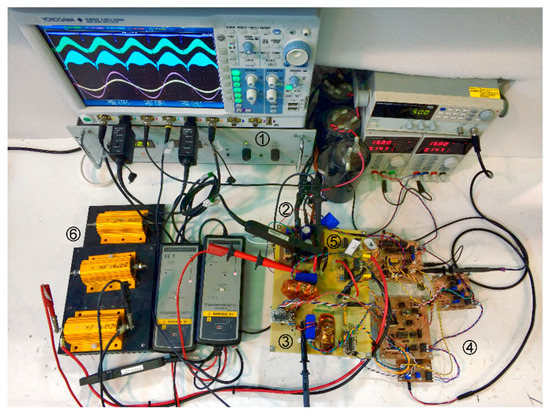
Figure 24.
Experimental setup and microinverter prototype.
The reference vref(t) is a rectified sinusoidal signal, provided by the ancillary circuit of Figure 22 that rectifies a sinusoidal voltage given by an external function generator.
The items displayed in Figure 24 are (1) the power supply SM70-45-D, (2) the buck-switch stage, (3) the two cascaded-boosts, (4) the ancillary and control PCBs, including both surfaces; (5) the unfolding stage; and finally the (6) load resistances (50–200 W). The oscilloscope, the function generator, and the power supply for the control boards are also shown.
Concerning the microinverter output waveforms, the results are very similar despite the control surface used or the hysteresis type. As both control surfaces are designed to do the same, a proof of their good performance is that the experimental results are practically identical.
The effect of the buck-switch to solve zero-cross distortion can be seen in Figure 25. The dark-blue color signal Vg is the quadratic-boost input voltage, the light-green signal is Vc1, the cyan signal is Vc2, the red one is the unfolding output voltage Vout, and finally the pink color signal is the reference voltage Vref. Realize that the introduction of the quadratic-boost supply allows that all voltage variables go to zero at crossing-instants reducing the distortion effects.
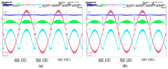
Figure 25.
Input current surface with constant-width hysteresis. Microinverter variables traces, (a) without the Buck-switch, and (b) including the Buck-switch.
A load transient from 50 to 150 W was carried out to see the dynamic response, and similar results were obtained for both surfaces. Constant or variable hysteresis width have no influence in dynamic response for input current surface case (Equation (7)). Nevertheless, the self-oscillating surface requires a very small hysteresis width when both current variables iL1 and iL2, are near to zero to start oscillating, and to avoid excessive switching losses a variable hysteresis width is used.
In the caption of Figure 26, the load current is the orange color signal, and the microinverter output voltage is depicted in red.
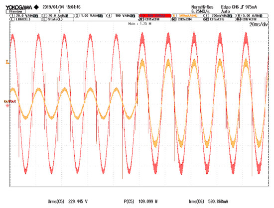
Figure 26.
Load transition of 50 to 150 W.
Next oscilloscope captions, see Figure 27, depict the experimental inverter waveforms at 100 W, for both surfaces and different hysteresis types to illustrate their effect on the inverter output. Captions are given in two types. On the left side, there is always the oscilloscope captions in sample mode. In the right side, we include the same experiment when the oscilloscope is averaging 256 samples. This allows to see the real averaged value of all the variables, neglecting their high-frequency ripple.
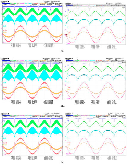
Figure 27.
Microinverter captions at 100 W under different conditions. (a) Input current control and constant hysteresis. (b) Input current surface and variable hysteresis, and (c) self-oscillating surface and variable hysteresis.
As can be seen in all the figures, the output voltage and current, shown in red and orange colors respectively, are always equal, despite the selected hysteresis and control surface type.
The input current iL1(t), depicted in light-green color, and the intermediate capacitor voltage vC1(t), in cyan color, show clearly the effect of the hysteresis type, as can be observed comparing the different ripple amplitudes in the left captions (sample mode). On the contrary, in the right side captions, where digital oscilloscope averaging is applied, the input current iL1(t) shows clearly a sin2(ωot) waveform type, whereas the vC1(t) exhibits a waveform of type |sin(ωot)|1/2, as expected from the state vector (Equation (6)) reproduced here in Equation (33).
Figure 28 and Figure 29, Figure 30 and Figure 31 give, respectively, the inverter efficiency, and the minimum and maximum switching frequency, and the average switching frequency for diverse output powers P(W) = {25, 50, 75, 100, 125, 150}. Different control surfaces and hysteresis types are used. The input current surface with variable hysteresis exhibits the best efficiency, around 90%.
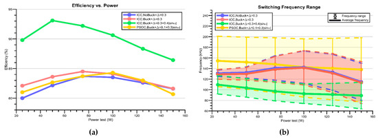
Figure 28.
Microinverter results at different output powers, (a) efficiency, and (b) switching frequency.

Figure 29.
Microinverter efficiency in %.
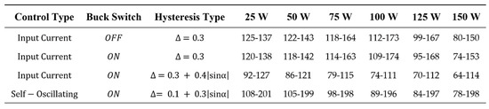
Figure 30.
Microinverter maximum and minimum switching frequency in kHz.
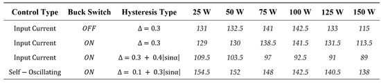
Figure 31.
Microinverter average switching frequency in kHz.
8. Conclusions
A quadratic-boot based microinverter is presented in this work. The first stage is a cascaded boost converter, and the second stage is a full-bridge. In the classical approach (slow-fast), the cascaded boost converter output is a 350–400 DC voltage that supplies a full-bridge inverter. This work explores a new alternative, the “fast-slow” strategy. In this approach, the first stage delivers a sinusoidal rectified voltage of 230 Vrms to the full-bridge unfolding stage to get the AC output.
Comparing both strategies, in the classical approach, the sinusoidal voltage is obtained by PWM modulation. Thus, the full-bridge stage must switch at high frequency to deliver a low THD sinusoidal output. In contrast, in the “fast-slow” approach the full-bridge is switching at 50 Hz, as operates as unfolding stage, and the switching losses of this stage are negligible.
If the first stage output voltage in both strategies is compared, in the classical approach this voltage is 350–400V, but for the approach presented here, the peak value is 325 V and its rms value is 230 Vrms. This means that the stress of the switching devices is lower, and therefore, at equal switching frequency, the switching losses will be lower.
Now, if the dynamics involved in both approaches are compared, in the classical approach, the microinverter plant has 6th order dynamics, whereas in the “slow-fast” approach, as the unfolding stage lacks the second order filter, and the plant has only 4th order dynamics.
Next, if PWM control is applied in the “slow-fast” case, three PI regulators are required to operate the inverter, two for the first stage (inner current loop and voltage loop) and the third PI for the full-bridge inverter voltage loop. This implies that the whole microinverter would have 9th order dynamics. Applying PWM control to the “fast-slow” strategy means two PI regulators for the first stage, the whole system becoming dynamics of the 6th order.
To conclude, it is important to remark that the dynamics of the cascaded-boost is highly nonlinear, and the small-signal output voltage to control transfer function, and therefore, the plant poles, depend strongly on the complementary converter duty cycle (D’ = 1-D). As a result, in the “slow-fast” approach the pole position is quite constant, and only depends on the input voltage variations. Oppositely, in the “fast-slow” approach, as the first stage output voltage is following a sinusoidal waveform, and the plant poles are continuously changing making practically impossible a classical control approach using PWM techniques.
Sliding mode control is a non-linear control technique with inherent robustness to parametric variations and perturbations, very simple to implement (only a hysteretic comparator is required), and it produces a system-order reduction. When this control technique is applied to the “fast-slow” microinverter, the 4th order plant, becomes a 3rd order one. Besides, to regulate the inverter output voltage, only one external loop is required, the first-stage PI controller. Thus, the closed-loop microinverter becomes finally a 4th order system.
Two different sliding control surfaces were proposed. An input current surface, and a self-oscillating surface. Both surfaces were analyzed, and the corresponding PI regulators were designed. The input current surface is relatively classic and is based on controlling the converter input energy. The converter with the self-oscillating approach behaves like a variable transformer, with ideal rejection of load and line disturbances, and directly establishes the sinusoidal output voltage. In fact, the voltage regulation loop is only required to compensate the converter losses.
The input current surface has a first order dominant pole at low output voltage that evolves to a pair of critically damped (ζ = 1) real poles, whereas the self-oscillating surface exhibits a second order dominance with a pair of undamped complex conjugated poles. At both surfaces the pole position is practically proportional to the mean load power, whereas the damping ratio increases with the output voltage. In addition, as the dominant pole (5·103–104 rad/s) of the input current surface is five times faster than the real part of the self-oscillating surface dominant poles (103–2·103 rad/s), the input current surface bandwidth is higher, and the closed-loop dynamic response is faster.
The validity of the proposed “fast-slow” approach with any of the proposed surfaces was demonstrated with several oscilloscope captions. Two types of hysteresis were considered, constant and variable. According to the experimental results, the input current surface with a variable hysteresis width exhibits the better efficiency results.
Author Contributions
Conceptualization, H.V.-B.; Data curation, E.R.-R. and X.G.-M.; Formal analysis, H.V.-B., E.R.-R. and C.O.; Funding acquisition, H.V.-B.; Investigation, H.V.-B., E.R.-R., C.O. and X.G.-M.; Methodology, H.V.-B. and C.O.; Project administration, H.V.-B.; Resources, H.V.-B.; Supervision, H.V.-B. and C.O.; Validation, H.V.-B., E.R.-R. and X.G.-M.; Visualization, H.V.-B., E.R.-R. and X.G.-M.; Writing—original draft, H.V.-B., E.R.-R., C.O. and X.G.-M.; Writing—review & editing, H.V.-B. and C.O.
Funding
This research was funded by the Spanish Agencia Estatal de Investigación (AEI) and the Fondo Europeo de Desarrollo Regional (FEDER) under research projects DPI2015-67292-R (AEI/FEDER, UE).
Conflicts of Interest
The authors declare no conflict of interest. The funders had no role in the design of the study; in the collection, analyses, or interpretation of data; in the writing of the manuscript, or in the decision to publish the results.
References
- Zhao, Z.; Xu, M.; Chen, Q.; Lai, J.-H.; Cho, Y. Derivation, analysis, and imlementation of a boost-buck coverter-based high-efficiency PV inverter. IEEE Trans. Power Electron. 2012, 27, 1304–1311. [Google Scholar] [CrossRef]
- Oldenkamp, H.; de Jong, I. The Return of the AC Module Inverter. In Proceedings of the 24th European Photovoltaic Solar Energy Conference, Hamburg, Germany, 21–25 September 2009; pp. 3101–3104. [Google Scholar]
- Hasan, R.; Mekhilef, S.; Seyedmahmoudian, M.; Horan, B. Grid-connected isolated PV microinverters: A review. Renew. Sustain. Energy Rev. 2017, 67, 1065–1080. [Google Scholar] [CrossRef]
- Choudhury, T.R.; Nayak, B. Comparison and analysis of cascaded and quadratic boost converter. In Proceedings of the IEEE Power, Communication and Information Technology Conference (PCITC), Bhubaneswar, India, 15–17 October 2015; pp. 1065–1080. [Google Scholar]
- Lopez, D.; Flores-Bahamonde, F.; Renaudineau, H.; Kouro, S. Double voltage step-up photovoltaic microinverter. In Proceedings of the 2017 IEEE International Conference on Industrial Technology, Toronto, ON, Canada, 22–25 March 2017; pp. 406–411. [Google Scholar]
- Fornage, M. Method and Apparatus for Converting Direct Current to Alternating Current. US Patent 7,796,412, 14 September 2010. [Google Scholar]
- Yuhao Luo, J. Alternating Parallel Fly Back Converter with Alternated Master-Slave Branch Circuits. US Patent App. 13/807,0532, 9 June 2011. [Google Scholar]
- Cáceres, R.O.; Barbi, I. A Boost DC-AC Converter: Analysis, Design, and Experimentation. IEEE Trans. Power Electron. 1999, 14, 134–141. [Google Scholar] [CrossRef]
- Sanchis, P.; Ursæa, A.; Gubía, E.; Marroyo, L. Boost DC-AC inverter: A new control strategy. IEEE Trans. Power Electron. 2005, 20, 343–353. [Google Scholar] [CrossRef]
- Flores-Bahamonde, F.; Valderrama Blavi, H.; Garcia, G.; Martinez Salamero, L. Análisis de un Ondulador Boost basado en Control en Modo Deslizamiento para Energías Renovables. In Proceedings of the SAAEI’s 14, Tangiers, Morocco, 25–27 June 2014. [Google Scholar]
- Galigekere, V.P.; Kazimierczuk, M.K. Analysis of PWM Z-Source DC-DC Converter in CCM for Steady State. IEEE Trans. Circuits Syst. I Regul. Pap. 2012, 59, 854–863. [Google Scholar] [CrossRef]
- Lopez Santos, O.; Martinez Salamero, L.; Garcia, G.; Valderrama Blavi, H. Robust Sliding-Mode Control Design for a Voltage Regulated Quadratic Boost Converter. IEEE Trans. Power Electron. 2015, 30, 2313–2327. [Google Scholar] [CrossRef]
- Lopez Santos, O.; Martinez Salamero, L.; Garcia, G.; Valderrama Blavi, H.; Sierra Polanco, T. Comparison of the Quadratic Boost Topologies Operating under Sliding-Mode Control. In Proceedings of the Brazilian Power Electronics Conference (COBEP), Gramado, Brazil, 27–31 October 2013. [Google Scholar]
- López Santos, O.; Martínez Salamero, L.; García, G.; Valderrama Blavi, H.; Mercuri, D.O. Efficiency Analysis of a Sliding-Mode controlled Quadratic Boost Converter. IET Power Electron. 2013, 6, 364–373. [Google Scholar] [CrossRef]
- Erickson, R.W.; Maksimovic, D. Fundamentals of Power Electronics, 2nd ed.; Kluwer Academic: Dordrecht, The Netherlands.
- Martinez-salamero, L.; Valderrama-blavi, H.; Giral, R. Self-Oscillating DC-to-DC Switching Converters with Transformer Characteristics. IEEE Trans. Aerosp. Electron. Syst. 2005, 41, 710–716. [Google Scholar] [CrossRef]
- Kocher, M.J.; Steigerwald, R.L. An AC-to-DC Converter with High Quality Input Waveforms. IEEE Trans. Ind. Appl. 1983, IA-19, 586–599. [Google Scholar] [CrossRef]
© 2019 by the authors. Licensee MDPI, Basel, Switzerland. This article is an open access article distributed under the terms and conditions of the Creative Commons Attribution (CC BY) license (http://creativecommons.org/licenses/by/4.0/).