1. Introduction
In portable and processor applications, there is a continuous demand for a fast output voltage transient response. Therefore, a lot of control strategies are proposed for different DC-DC power converters. Among many strategies, the well-known
V2 controls have been widely used in industrial applications, and they can achieve a great control loop bandwidth [
1,
2,
3]. Predictive controls acquire state variables ahead of time, which allow earlier actions to stabilize the system [
4,
5]. Adaptive controls can achieve optimized performance in different conditions, which is ensured by online tunings for control parameters [
6,
7]. Current mode controls are effective approaches to simplify compensator design, and they can achieve fast transient performance with over current protection [
8,
9,
10]. Multiloop controls are popular for their closed-loop stability and flexible load/line transient optimizations [
11,
12]. Sliding mode and hysteretic controls are non-linear strategies to optimize large-signal transient responses, and they are not only robust to parameter deviations, but also easy for implementation [
13,
14,
15].
To achieve time-optimal output voltage transient responses, various control strategies have recently been investigated, such as time-optimal sliding-mode control [
16,
17], bang-bang and geometric control [
18], programmable deviation current control [
19], etc. Among many strategies, a practical approach to achieve time-optimal control is through capacitor charge balancing method [
20,
21,
22]. These controls adopt variable switching-on and switching-off durations to balance the charge on output capacitor, and achieve optimal output voltage transient response. Furthermore, various methods are proposed to carry out the control with digital circuits [
23,
24,
25,
26]. However, these control strategies induce a variable switching frequency, which challenges the converter modeling and EMI suppression [
27,
28]. Besides, all above charge balance controls are limited for buck converters operating in continuous conduction mode (CCM).
When a converter operates in discontinuous conduction mode (DCM), the discontinuous inductor current provides potential advantages of high stability, simple compensation, compact and low-cost inductor, etc. [
29,
30]. For DC-DC converters operating in DCM, a novel control strategy based on estimation and charge balance principle is proposed in [
31]. This forms the discrete charge balance (DCB) control where all control variables are updated once every cycle. The approach is based on digital pulse wide modulation (DPWM) with a fixed switching frequency, and suits various converters, such as boost and flyback converters, etc. Furthermore, with comprehensive consideration of parasitics, the control accuracy is improved in [
32,
33]. However, all above DCB algorithms are non-linear, and they induce complicated calculations. Besides, the calculations must be carried out in serial, i.e., charge estimation, charge compensation and charge regulation. These not only increase the hardware cost, but also cause considerable calculation lag that limits the switching frequency.
In order to solve above mentioned issues, a linearized discrete charge balance (LDCB) control strategy is proposed in this paper, which is acquired through linearizing conventional DCB controller. By deriving the differential functions of the DCB algorithm, the small signal relationship between the input and output of DCB controller is explored. Furthermore, the LDCB controller is formed through three independent feed loops, where the outputs are summarized as duty ratio. In this way, the LDCB controller eliminates several complicated calculations, such as divisions and square roots. Besides, since the relationship between the input and output is explicitly revealed, all loops can be carried out in parallel. Both the simplified algorithm and the parallelism help to save the hardware cost, reduce the calculation lag, and provide potential to improve the switching frequency. Furthermore, since the LDCB controller shares the same small signal model as that of DCB controller, it achieves similar control loop bandwidth and transient performance. The stability and robustness under LDCB control are proved by closed-loop modeling, transient analyses and zero/pole plots.
The paper is organized as follows. In
Section 2, control scheme and algorithm of the conventional DCB control strategy is introduced. The proposed LDCB controller is given in
Section 3, where the small signal relationship between the input and output of DCB controller is explored. In
Section 4, detailed closed-loop modeling under LDCB control is derived. Furthermore, the stability and robustness are proved by zero/pole plots and transient analyses. Experimental results and comparisons are given in
Section 5 to verify effectiveness of the proposed LDCB controller. Finally, a brief conclusion is given in
Section 6.
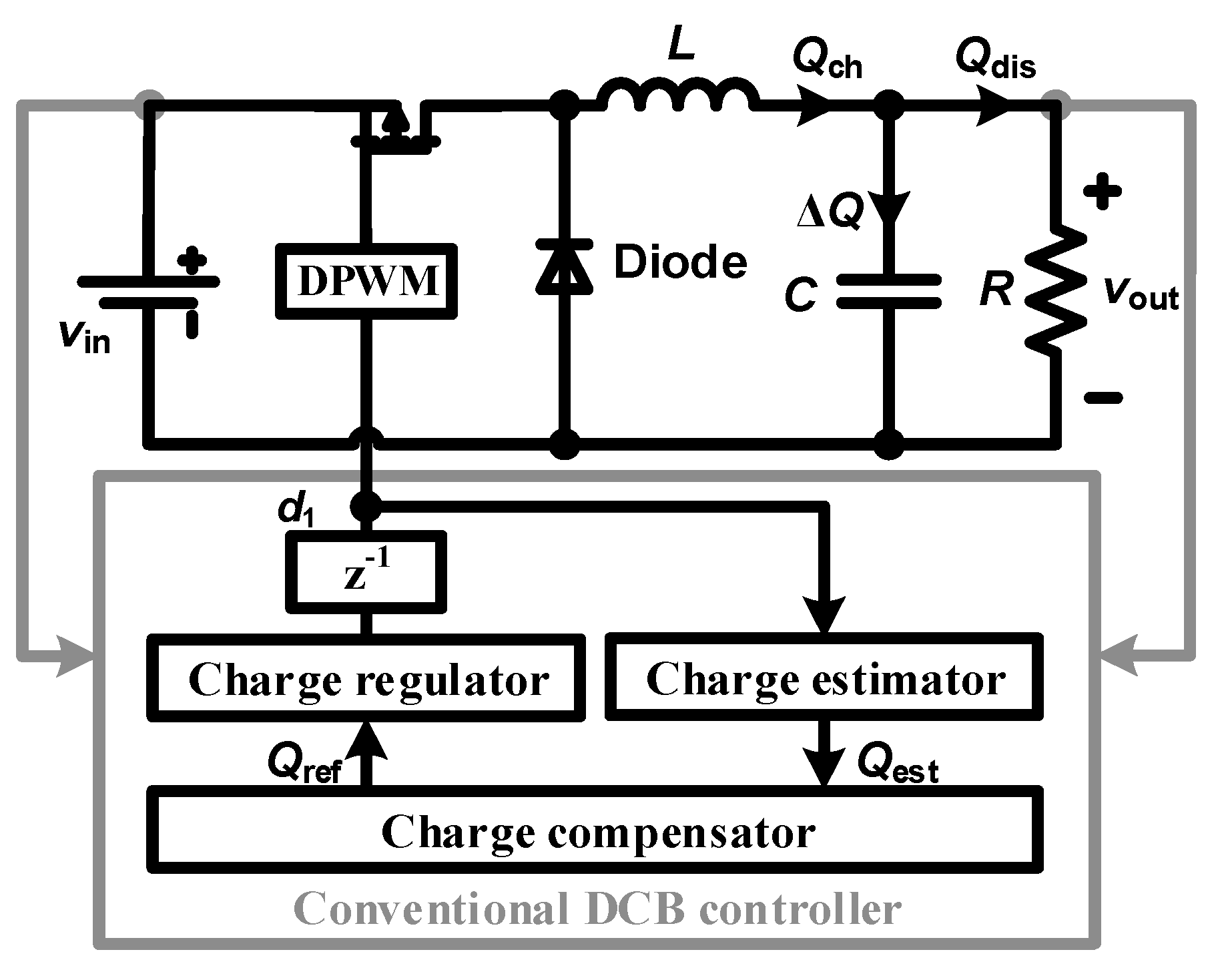
2. Conventional Discrete Charge Balance Control
For switched mode power converters, the output capacitor is charged and discharged periodically. At steady state, the charge and discharge are equal, which ensures a constant output voltage. When operating in DCM, the charge can be strictly controlled by the duty ratio of DPWM signal. Therefore, the output voltage can be controlled by balancing the charge on the output capacitor [
31,
32,
33]. This forms the DCB control strategy, and a buck converter under conventional DCB control is shown in
Figure 1.
The DCB controller consists a charge estimator, a charge compensator and a charge regulator. First, the charge estimator calculates the charge to output capacitor, denoted as the estimated charge . An appropriate charge estimator ensures that , where is the actual output charge. Second, to balance the charge on output capacitor, the charge compensator outputs a reference for output charge, denoted as . Algorithm of the compensator determines the output voltage transient responses to load and input. Finally, the charge regulator adjusts a suitable duty ratio to ensure that tracks in the next switching cycle.
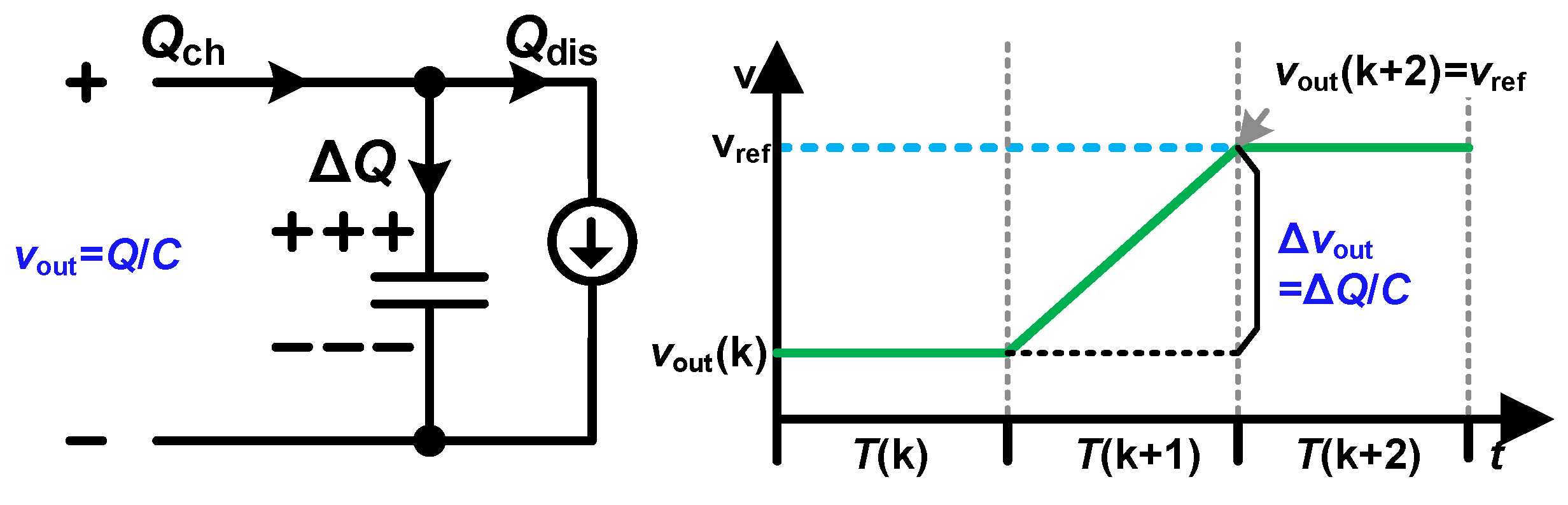
As shown in
Figure 2, the output voltage is controlled by increasing or decreasing the charge on output capacitor. Since the voltage across the capacitor is
, the voltage increment is given by
where
is the discharge of the capacitor. Furthermore,
can be regulated by
since
varies slow owing to the filtering effect of
. For example, when
is lower than
in the
switching cycle, the DCB controller increases
to generate a positive
. Finally, the output voltage is regulated to its reference value in the
switching cycle.
2.1. Charge Compensator
The charge compensator regulates the output voltage by compensating the charge on output capacitor. For discrete-time analyses, the voltage increment
is transformed as
Since the discharge is determined by
, (1) is derived as
Furthermore, iterating (2) gives
Nevertheless, is comparable to the output voltage ripple ratio, which is much smaller than unity in most DC-DC applications [
34], thus (3) approximates
To regulate the output voltage to its reference value in the
switching cycle, the charge compensator should provide a reference charge
that ensures
. Therefore, taking
,
and
into (4) gives
Based on (5), a reference charge for the switching cycle is calculated, which makes the output voltage tracking the reference voltage in two switching cycles. Furthermore, to carry out the algorithm in (5), a charge estimator must be derived to estimate , while a charge regulator should also be provided to calculate an appropriate .
2.2. Charge Estimator and Charge Regulator
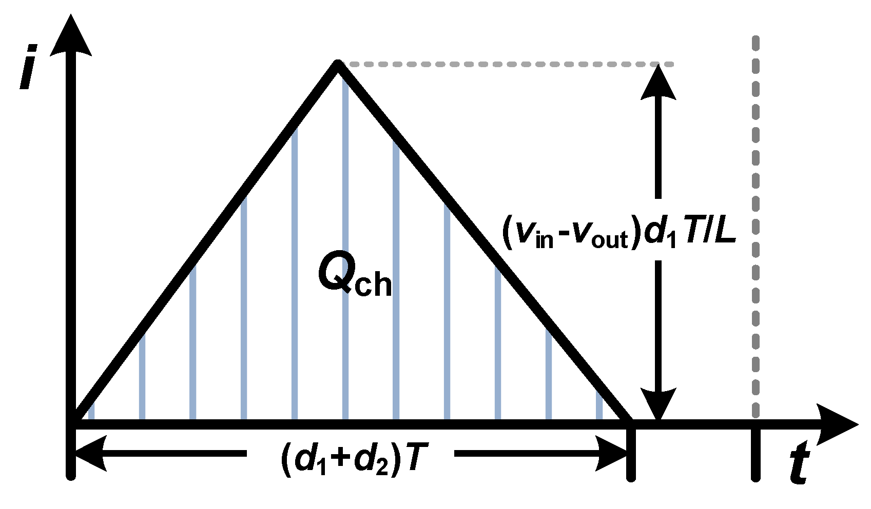
The DCB controller carries out charge estimation, charge compensation and charge regulation in serial. The charge estimator is required to estimate the output charge, while the charge regulator is needed to calculate an appropriate duty ratio. For DCM buck converter, the output charge in a switching cycle is determined by the inductor current. As shown in
Figure 3, the inductor current rises linearly when the main switch is on, and it falls linearly when the main switch is off.
The output charge is the integration of inductor current, i.e., the shadow area in
Figure 3. For buck converter, the inductor current peak value is
while
is always valid. Therefore, the output charge is given by
Based on (6), the charge estimation and regulation algorithms are derived as
These algorithms can ensure accurate charge estimation and charge regulation under DCM operation. However, they are relatively complicated owing to the square-root and division operations. Besides, the charge compensator and charge regulator are dependent on the charge estimator, thus the calculations must be processed in serial. These not only increase the hardware cost, but also cause considerable calculation lag that limits the switching frequency.
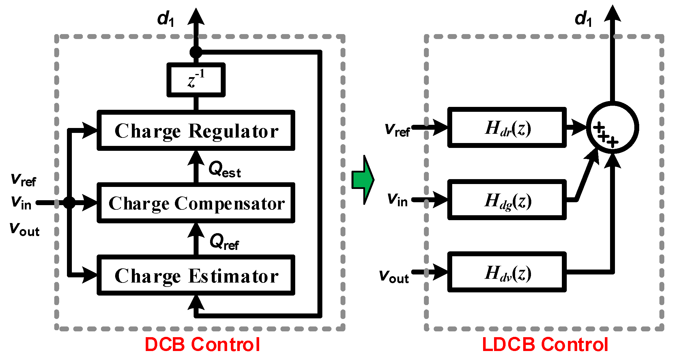
3. Linearized Discrete Charge Balance Control with Simplified Algorithm
Although conventional DCB controller can greatly optimize the control loop bandwidth and the output voltage transient response, it suffers a complicated algorithm and the serial calculations. These greatly increase the overall cost and the requirement for a high-performance digital control unit. A large calculation lag also limits the achievable switching frequency.
In order to solve above mentioned issues, the LDCB controller is proposed in this section. By deriving the differential functions of the DCB control algorithm, small signal relationship between the input and output of DCB controller is explored. Furthermore, the LDCB controller is formed through three independent feed loops, where the outputs are summarized as duty ratio. In this way, the LDCB controller eliminates several complicated calculations, such as divisions and square roots. Since the relationship between the input and output is explicitly revealed, all loops are carried out in parallel. Both the simplified algorithm and the parallelism help to save the hardware cost, reduce the calculation lag, and provide potential to improve the switching frequency.
3.1. Linearization of Conventional DCB Controller
To linearize DCB control, a partial differential function
is derived from the charge estimator, charge compensator, and charge regulator. Based on (7), differential function of the estimated charge is given by
where
,
and
denote partial differential functions
,
and
, respectively.
Since the charge controller uses
to calculate
, similar differential function is derived for the charge regulator:
In (9), a unit delay
is induced, since the duty ratio is pre-calculated for the next switching cycle. Furthermore, based on (5), differential function of
is given by
Finally, combining (8)–(10), a partial differential function
is derived as
This equation explicitly reveals the relationship between and . Based on (11), the LDCB controller can be realized by three independent feedback and feed forward loops.
3.2. Realization of LDCB Control
Similar to conventional DCB control, the LDCB controller regulates the output voltage with three inputs, i.e.,
,
and
. Each of the inputs has an independent feeding loop to
, as shown in
Figure 4.
Furthermore, since the LDCB controller maintains the same small signal model as conventional DCB controller, it achieves similar control loop bandwidth and transient performance. Besides, without calculating state variables (such as
and
), the LDCB controller has a simplified algorithm and features parallel calculations, as shown in
Table 1.
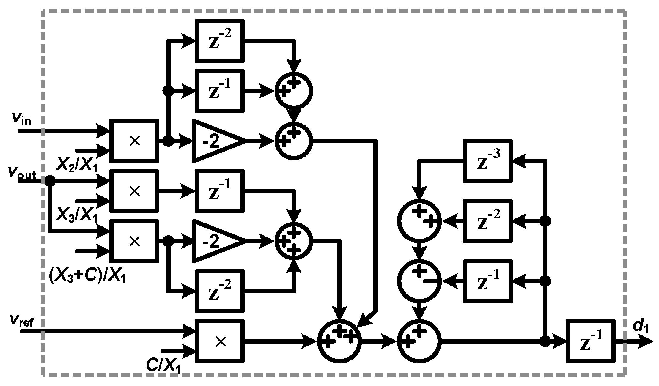
Based on (11), a further simplified implementation of LDCB controller is given in
Figure 5. This implementation requires only six multipliers and nine adders. Moreover, all feeding loops calculations are processed in parallel, which greatly reduces the calculation lag. Therefore, compared with conventional DCB controller, the LDCB controller can reduce the hardware cost, while providing potential for a higher switching frequency.
4. Closed-Loop Analysis and Robustness of LDCB Controller
To verify the stability under LDCB control, closed-loop small signal model is derived to investigate zeros and poles of the system. Since the LDCB controller is derived through linearizing conventional DCB controller, they share the same closed-loop small signal model at the typical operation point. However, when the operation point deviates, the system under LDCB control may fail owing the deviated model. Therefore, robustness of LDCB controller is further verified with ±30% deviation of the operation point. Since the controller is digital, all analyses and simulations are carried out in discrete-time domain.
4.1. Closed-Loop Small Signal Model
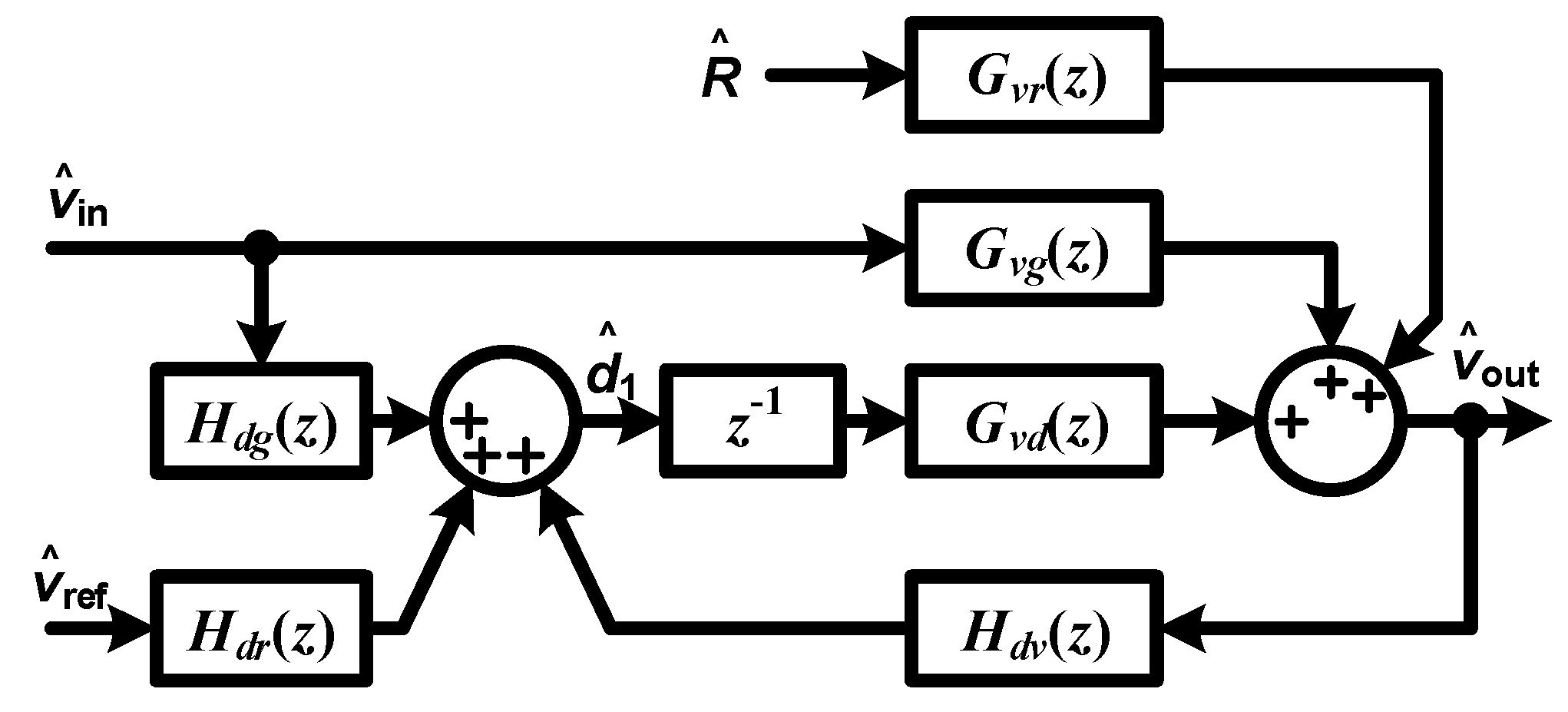
Since
,
and
are independent variables in a DC-DC converter, their impacts to
are modulated by three transfer functions, namely
,
and
, respectively. Under LDCB control, the duty ratio is acquired through
. Therefore, the closed-loop small signal model under LDCB control is given by
Figure 6.
Based on transfer function of the output filtering network, the relationship between
and
is given by
Based on (12), differential function of
is given by
Furthermore, to derive the discrete-time transfer functions, (13) is transformed to its
z domain, as shown in (14).
where
. Since the charge to output is
, substituting
into (14) gives
Obviously, all the functions are first-order, and they share the same pole. Furthermore, based on
Figure 6, closed-loop transfer functions from input voltage, reference voltage and load to the output voltage are given by
Substituting (15) and (11) into (16) gives
This discrete-time closed-loop model reveals the output voltage responses to different signals, i.e., input voltage, reference voltage and load resistance.
4.2. Stability Analysis
Substituting
into (17) gives out an explicit form of the closed-loop model, as shown below
where
M denotes
. Furthermore, the discrete-time responses to input voltage, reference voltage and load are solved by introducing an input of unit step signal
, as shown below
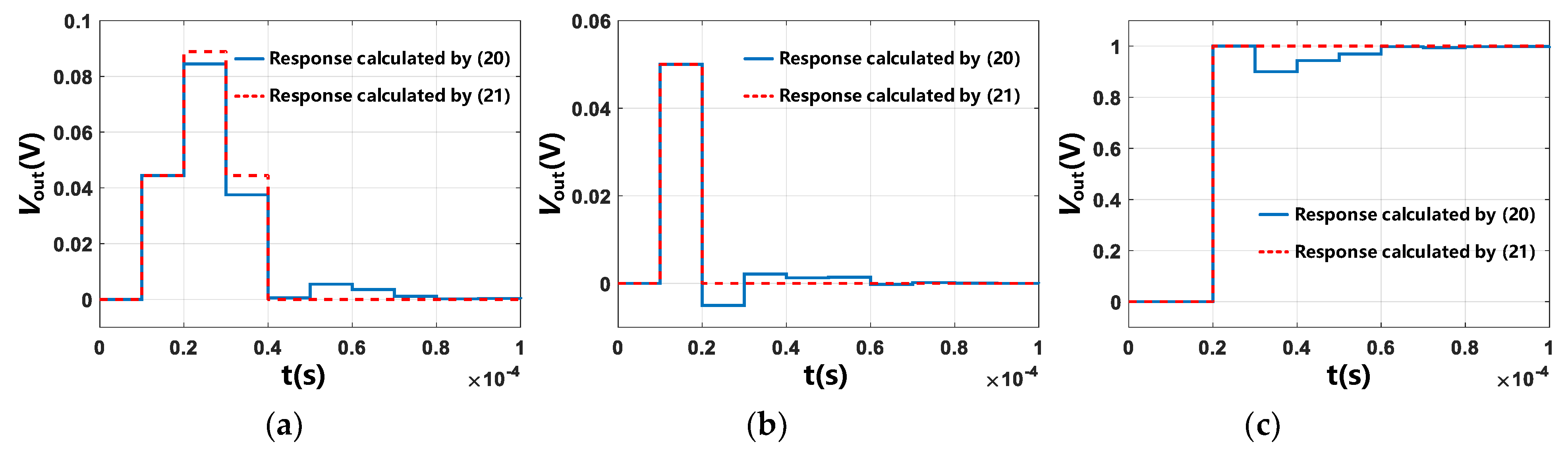
Through synthetic division, the discrete-time responses are derived as (20). Without approximation, (20) provides accurate analyses for different transients. It indicates that the output voltage will stabilize in five switching cycles during an input voltage step, five switching cycle during a reference voltage step, and seven switching cycles during a load step.
To reveal the main characteristics of the transients, most items that contains
are neglected, since magnitude of
is usually much smaller than unity. Furthermore, the discrete-time transient responses approximate
Although (21) is less accurate than (20), it reveals the main characteristics of (20). According to (21), when the load steps by a unit, the output voltage deviates by maximum, and stabilizes in three switching cycles. When a unity step of input voltage occurs, the output voltage will deviate by and it lasts for only one switching cycle. When the reference voltage steps, the output voltage tracks it and stabilizes in two switching cycles.
Furthermore, based on specifications in
Section 5, different transients are calculated from (20) and (21), respectively. As shown in
Figure 7, both approaches derive similar results. Comparatively, (20) is more accurate and it shows details, while (21) reveals the main characteristics of (20). During an unit
R step, the output voltage deviates by 0.085 V and re-stabilizes in seven switching cycles. During an unit
vin step, the output voltage deviates by 0.05 V, and re-stabilizes in six switching cycles. During an unit
vref step, the output voltage tracks
vref in five switching cycles.
4.3. Robustness to Deviated Operation Point
Although the LDCB and DCB controls have the same small signal model at the typical operation point, they are not equivalent when the operation point is deviated. Therefore, the robustness of LDCB controller must be verified with deviations of input voltage, output voltage and load.
Closed-loop small signal model of the system under deviated operation point is given in
Figure 8. The LDCB controller is modeled at a fixed operation point of
, whereas the main power stage operates at a deviated point of
.
Based on specifications in
Section 5, the typical operation point is at
, and the LDCB controller is derived with this point. However, the power stage can operate at other conditions. Thus, it is modeled with more than
deviations of operation point, i.e.,
,
,
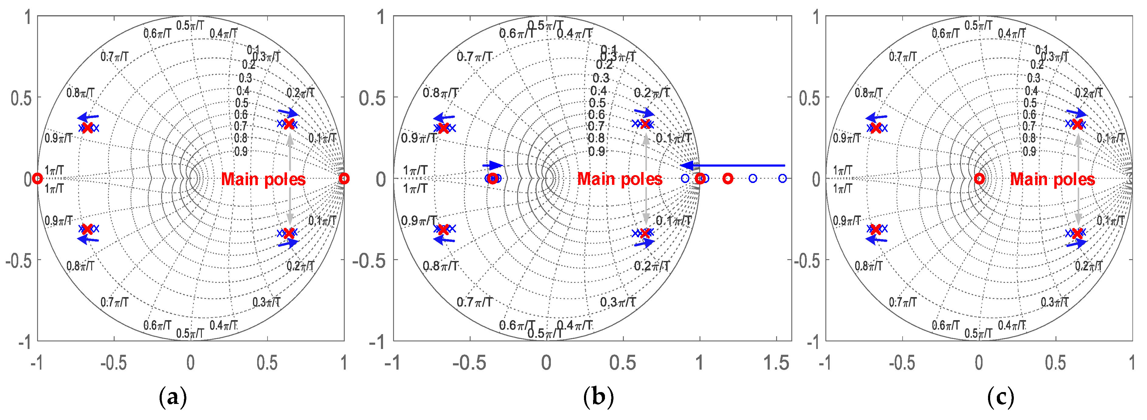
. The mismatched operation point causes change of the closed-loop model, which is simulated to verify the robustness of LDCB controller. With deviated operation point, zeros and poles of
,
and
are plotted in
Figure 9,
Figure 10 and
Figure 11 respectively.
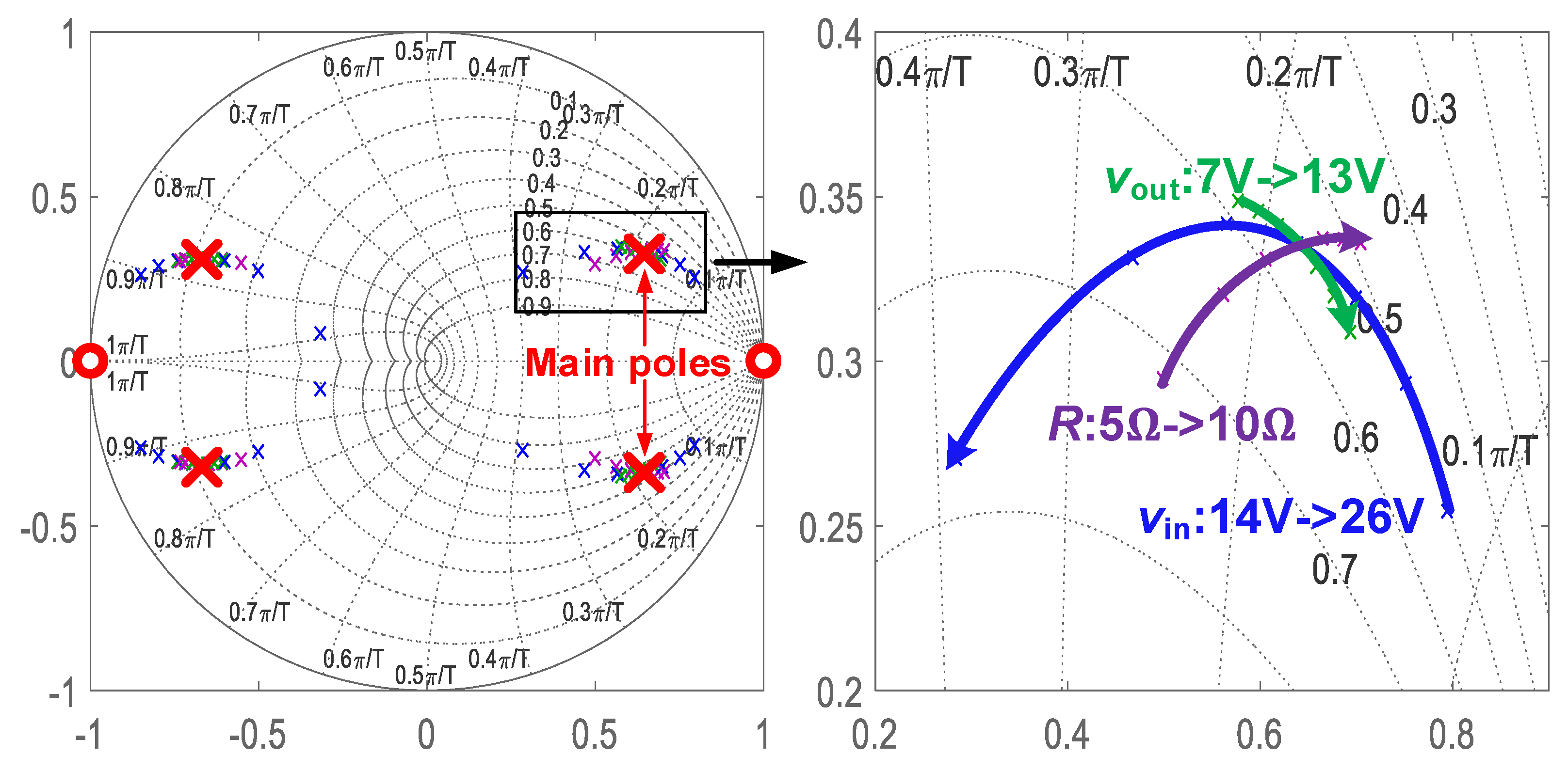
As shown in
Figure 9, two main poles of
Fvl(
z) locate at 0.639 ± j0.336, which are conjugate and they dominate the output voltage transient response to a load step. When the input voltage increases from 14 V to 26 V, migrations of the main poles indicate a higher bandwidth and damping factor. When the load resistance and output voltage changes by ±30%, variations of the main poles are relatively small. A zero at
z = 1 shows that
, which indicates zero DC gain to load. Therefore, the output voltage steady state value is not influenced by the load resistance.
Under the same deviations of operation point, zeros and poles of
are given in
Figure 10. Migrations of two main poles are exactly the same as those in
Figure 9. A zero at
z = 1 indicates that
or differential characteristic, thus the output voltage steady state value is not influenced by the input voltage.
Zeros and poles of
under the same deviations are given in
Figure 11. Migrations of the two main poles are exactly the same as those in
Figure 9 and
Figure 10. For
, substituting
z = 1 into (18) gives
, which indicates unity DC gain to the reference voltage. Therefore, the output voltage tracks
vref at steady state.
All above plots share the same poles, where two main poles indicate that the achieved bandwidth is about 0.18π/
T. This bandwidth is relatively high for DC-DC applications, and it suggests a transient response time around 0.35/(0.18π/
T) ≈ 6
T. This matches with that of the results in
Figure 7.
4.4. Robustness to Inductance Deviation
In order to verify the LDCB control robustness to inductance deviation, zero/pole trajectories are simulated when the inductance deviates from 0.8
L to 1.2
L, as shown in
Figure 12.
In all simulated results, the poles remain inside the unit cycle, and the variations are relatively small. This indicates that inductance deviation has minor influences to the output voltage transient responses. For both Fvl(z) and Fvg(z), the zero at z = 1 is not changed, which indicates zero DC gain to load and line voltage. Therefore, with deviated inductance, the output voltage steady state value is still not influenced by load and line voltage. For Fvg(z), a zero outside the cycle moves inside, which changes the gain at low frequency. However, the influence to line transient is minor, since line transient is dominated by the main poles. All results prove that LDCB control is capable to maintain the transient performance with inductance deviation of ± 20%, which is an adequate margin for most inductors.
5. Experimental Results
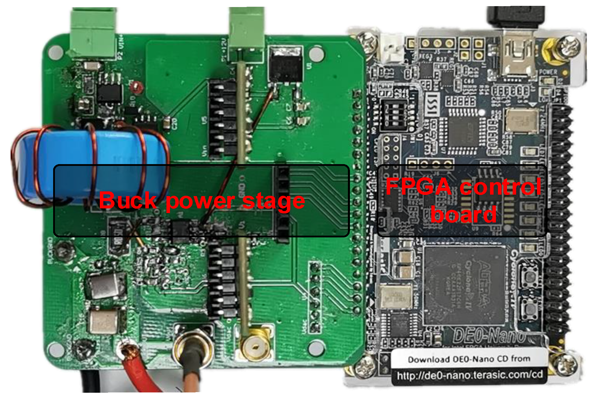
All analyses and simulations prove the stability and robustness of the converter under LDCB control. The results indicate a fast and stable transient response. In this section, transient performance of the converter is further verified through experiments. A buck converter prototype is constructed as the power stage, and the main specifications are given in
Table 2.
The switching frequency is 100 kHz, and the converter operates at DCM. A photograph of the prototype is shown in
Figure 13. The control board adopts a FPGA (Cyclone IV EP4CE22F17C6) to carry out all control algorithms. The input and output voltages are sampled by ADC LTC2314.
In the following, different transients under conventional proportion-integral (PI) control, DCB control and LDCB control are compared. Furthermore, the hardware and calculation lags under different controls are also compared.
5.1. Output Voltage Transient Responses under Different Controls
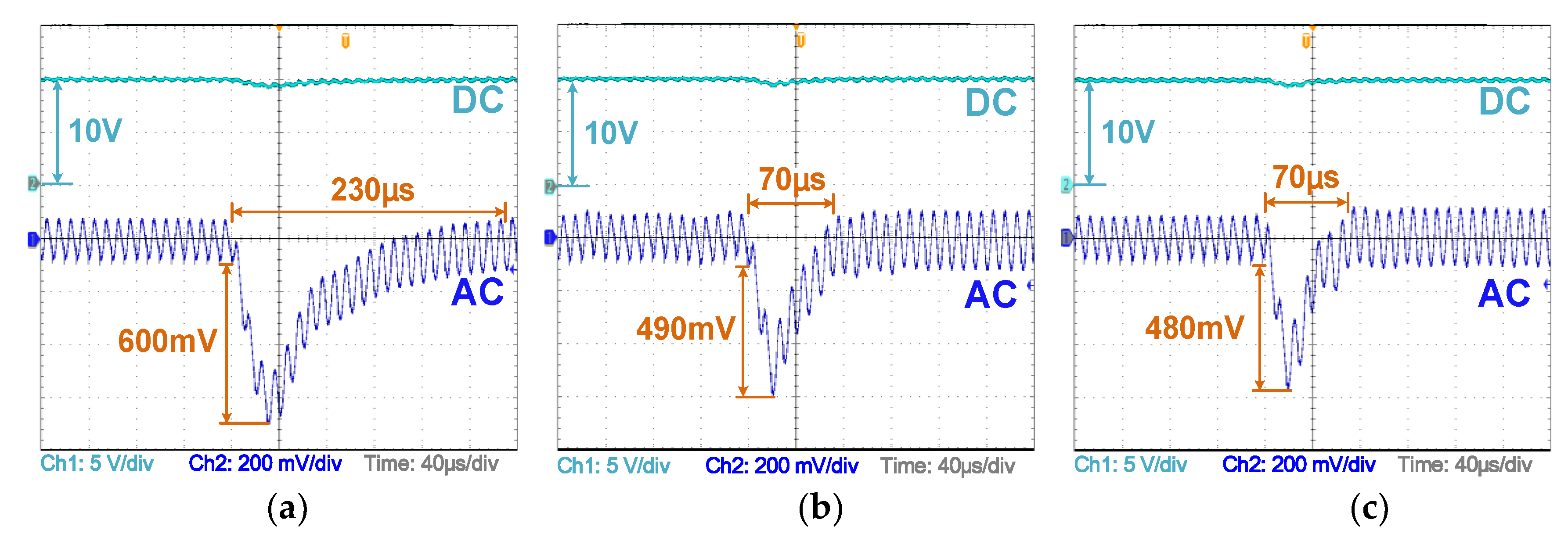
The output voltage transient responses to load under different controls are verified when
R steps from 10 Ω to 5 Ω. According to analyses in
Section 4, the output voltage under LDCB control deviates by 0.085 V maximum under a unit
R step, and it re-stabilizes in seven switching cycles. Therefore, the output voltage is expected to deviate by −0.43 V maximum when
R steps from 10 Ω to 5 Ω, and it should re-stabilize in 70 μs. The experimental results are given in
Figure 14. With PI control, the output voltage deviates by −0.6 V maximum, and it re-stabilizes in 230 μs. The DCB and LDCB controls achieve similar transient performance. Under either control, the output voltage re-stabilizes in 70 μs, while the maximum deviations are very close. The results match with that of analyses in
Section 4.
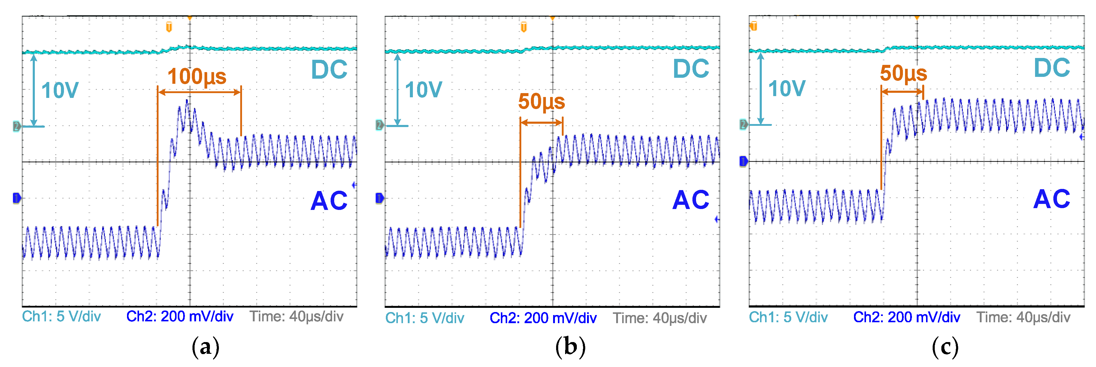
The output voltage transient responses to input voltage under different controls are verified when vg steps from 20 V to 18 V, as shown in
Figure 15. With PI control, the output voltage deviates by −0.24 V maximum, and it re-stabilizes in 130 μs. Based on analyses in
Section 4, the output voltage under LDCB control should deviate by −0.1 V maximum when vin steps from 20 V to 18 V, and it should re-stabilize in 60 μs. In the experiment, both DCB and LDCB controllers achieved very small output voltage deviations. The results highly match with that of simulations and analyses. With DCB and LDCB controls, the output voltage returns to 10 V in two switching cycles. After a minor oscillation, it re-stabilizes in 70 μs and 60 μs, respectively.
Output voltage transient responses to the reference voltage under different controls are verified when
vref steps from 10 V to 10.5 V, as shown in
Figure 16. With PI control, the output voltage tracks
vref in 80 μs, and an overshoot of 0.2 V, i.e., 40 %, is induced. The DCB and LDCB controllers achieve similar results in this transient. Both output voltages track
vref in 50 μs, and the result matches with that of analyses in
Section 4.
5.2. Hardware and Lag Analyses for Different Control Algorithms
Both DCB and LDCB controllers achieve much better transient performance than that of PI controller. Compared with DCB control, advantage of the proposed LDCB controller mainly lies in its simplified algorithm and improved parallelism, which save the hardware cost and reduce the calculation lag. Detailed comparisons of hardware and calculation lags under different controls are given in
Table 3. All algorithms have been optimized with the least calculations, and they are based on the same FPGA control board, i.e., Cyclone IV EP4CE22F17C6 (operating at 200 MHz).
Conventional PI controller induces the minimum calculations, i.e., three adds and two multiplies, which results in the least hardware cost, i.e., 2575 logic elements and 1866 registers. The DCB control algorithm is complicated owing to the division and square root calculations, which lead to the highest hardware cost, i.e., 4339 logic elements and 3109 registers. The LDCB controller requires nine adds and six multiplies, resulting in a medium hardware cost of 2964 logic elements and 2232 registers. Compared with conventional DCB controller, the LDCB controller reduces the hardware cost by 31.7% in logic elements and by 28.2% in registers. Furthermore, although LDCB controller requires 15 calculation elements, i.e., nine adds and six multiplies, 12 of them can be carried out in parallel. The parallelism of LDCB controller results in the least calculation lag of 275 ns, which is even less than that of PI controller. The overall lag is 575 ns, which provides potential for the highest switching frequency of 1.7 MHz.
As a conclusion, the proposed LDCB controller achieves similar transient performance to that of DCB controller. While algorithm of LDCB controller is simplified, resulting in a reduced hardware cost and calculation lag. Furthermore, the reduced lag provides potential for a higher switching frequency under the same hardware speed.
6. Conclusions
This paper presents a LDCB control strategy for DCM buck converter. The control algorithm and scheme are derived through linearizing conventional DCB controller. Since the LDCB controller has the same small signal model as that of DCB controller, it achieves similar control loop bandwidth and transient performance. Furthermore, benefiting from the simplified algorithm and parallel calculations, the LDCB controller provides advantages of a simplified algorithm and a reduced calculation lag. Compared with conventional DCB controller, the hardware cost is greatly reduced, where the logic elements are reduced by 31.7%, and the registers are reduced by 28.2%. Besides, the calculation lag is decreased from 600 ns to 275 ns, which provides potential for a higher switching frequency. The stability under LDCB control is verified by closed-loop analyses, while ±30% deviation of operation point and ±20% deviation of inductance are introduced. In all deviated conditions, migrations of the main poles are relatively small, which prove the robustness of LDCB control. Finally, experimental results shown that the proposed LDCB controller achieves similar transient performance to DCB controller. While compared with conventional PI controller, the LDCB controller reduces the transient response time by more than 50%.


