Author Contributions
Conceptualization, H.V.-B.; methodology, H.V.-B. and M.M.-R.; software, M.M.-R.; validation, H.V.-B., M.M.-R., and C.R.; formal analysis, H.V.-B., M.M.-R., and C.R.; investigation, H.V.-B. and M.M.-R.; resources, H.V.-B., M.M.-R., and C.R.; data curation, M.M.-R.; writing—original draft preparation, H.V.-B., M.M.-R., and C.R.; writing—review and editing, H.V.-B., M.M.-R., M.R., and C.R.; visualization, H.V.-B., M.M.-R., M.R., and C.R.; supervision, H.V.-B.; project administration, H.V.-B.; funding acquisition, H.V.-B.
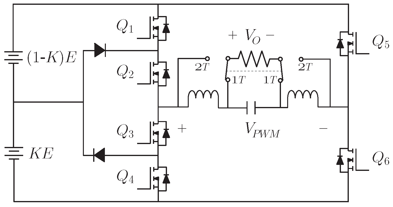
Figure 1.
Asymmetric full-bridge multilevel inverter (AFBMI).
Figure 1.
Asymmetric full-bridge multilevel inverter (AFBMI).
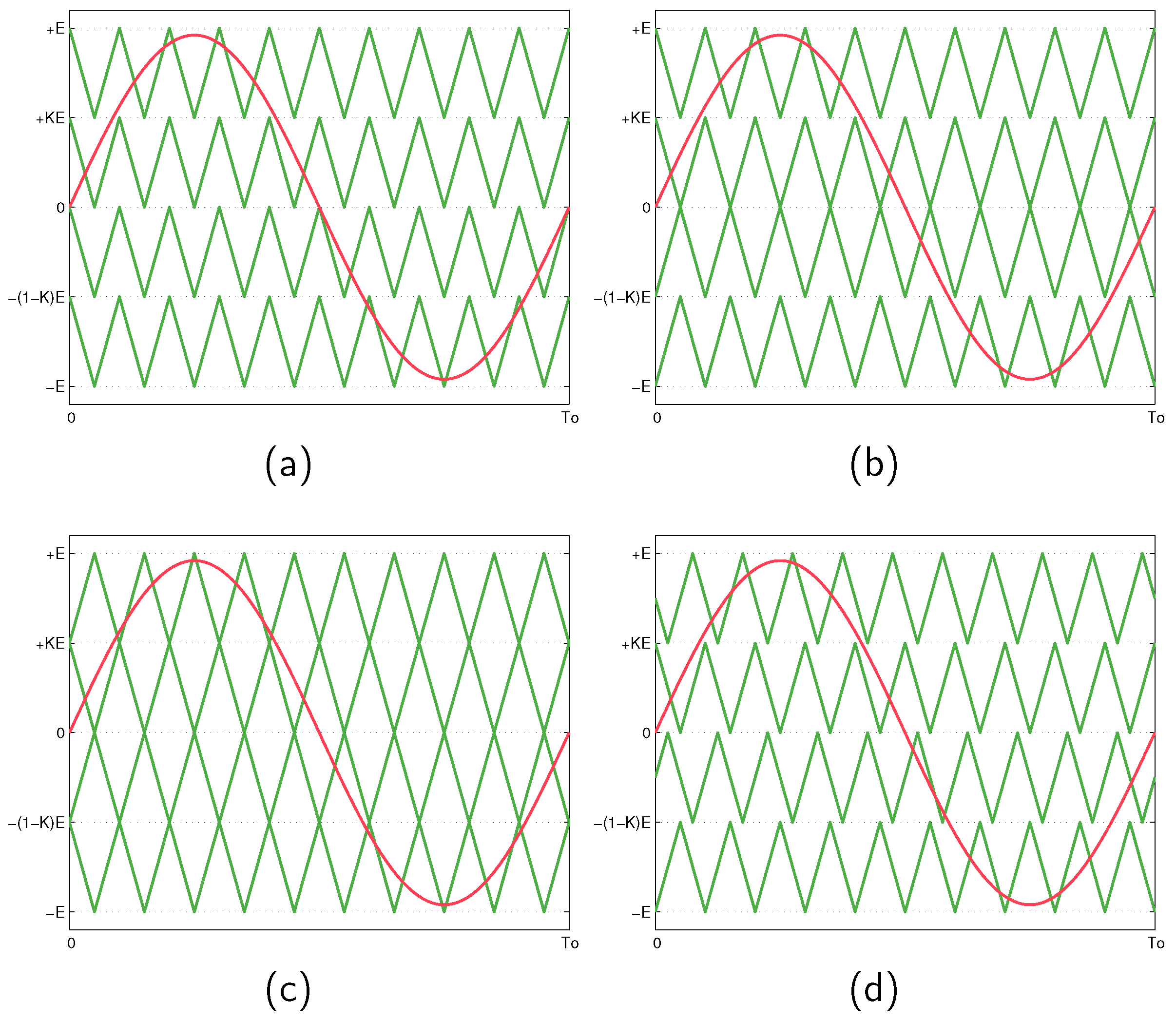
Figure 2.
Types of disposition for vertical multicarrier sinusoidal pulse width modulation (SPWM): (a) phase disposition (PD), (b) phase opposition disposition (POD), (c) alternative phase opposition disposition (APOD), and (d) phase shift (PS). In the vertical axis, there are carriers for N levels. is selected for the horizontal axis for the sake of easiness. Note that there are switching intervals. Only one of the carriers is active for comparison with the modulating signal .
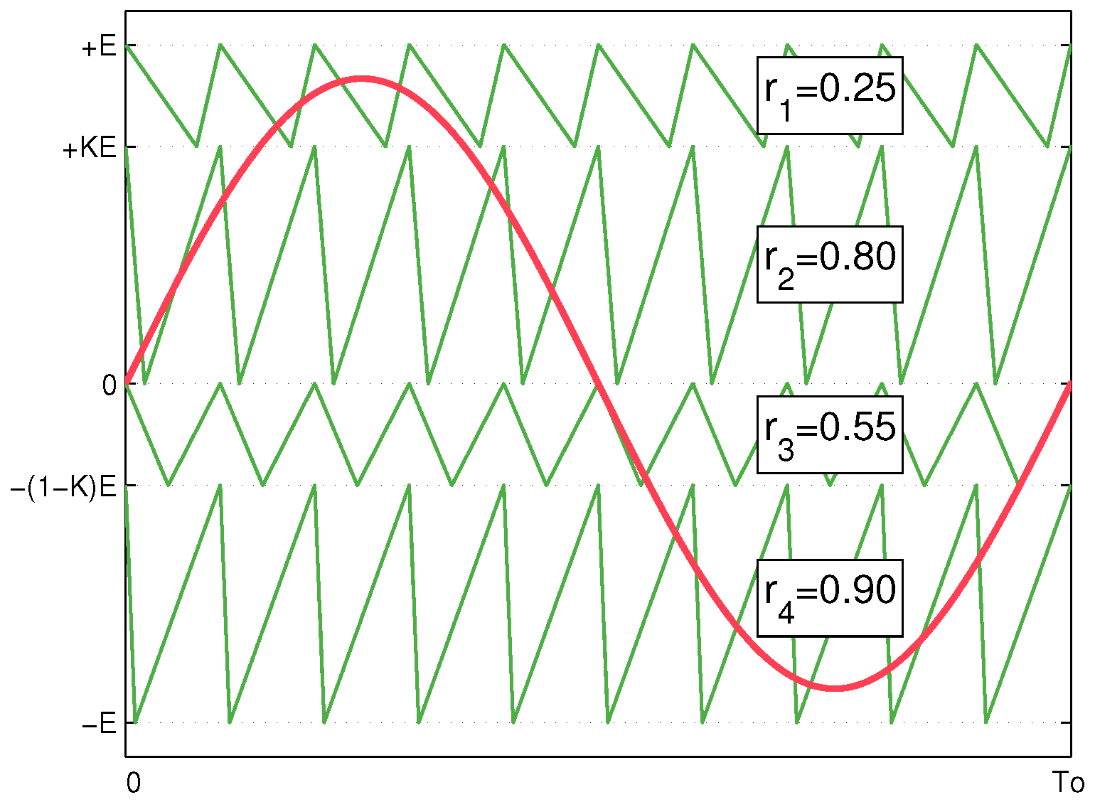
Figure 3.
Five-level PD-SPWM with modified carrier slopes: Note that the carrier ratios do not represent standard carriers. Each carrier controls one switching zone as follows: , , , and .
Figure 3.
Five-level PD-SPWM with modified carrier slopes: Note that the carrier ratios do not represent standard carriers. Each carrier controls one switching zone as follows: , , , and .
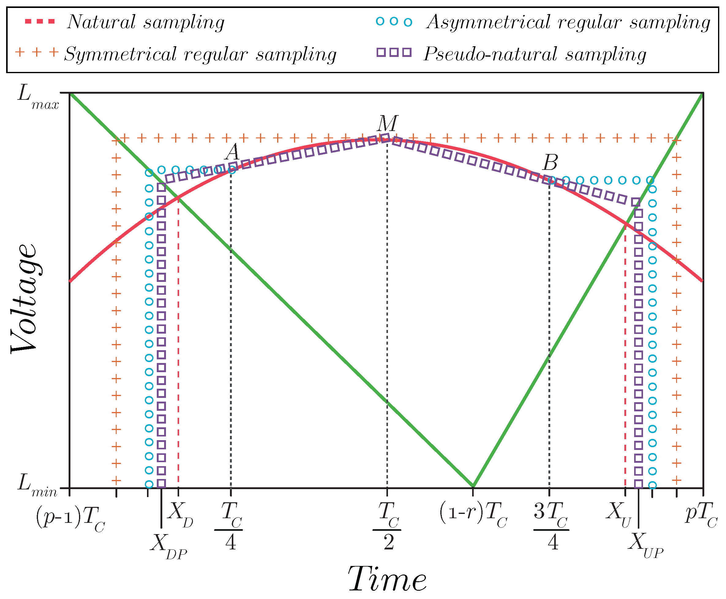
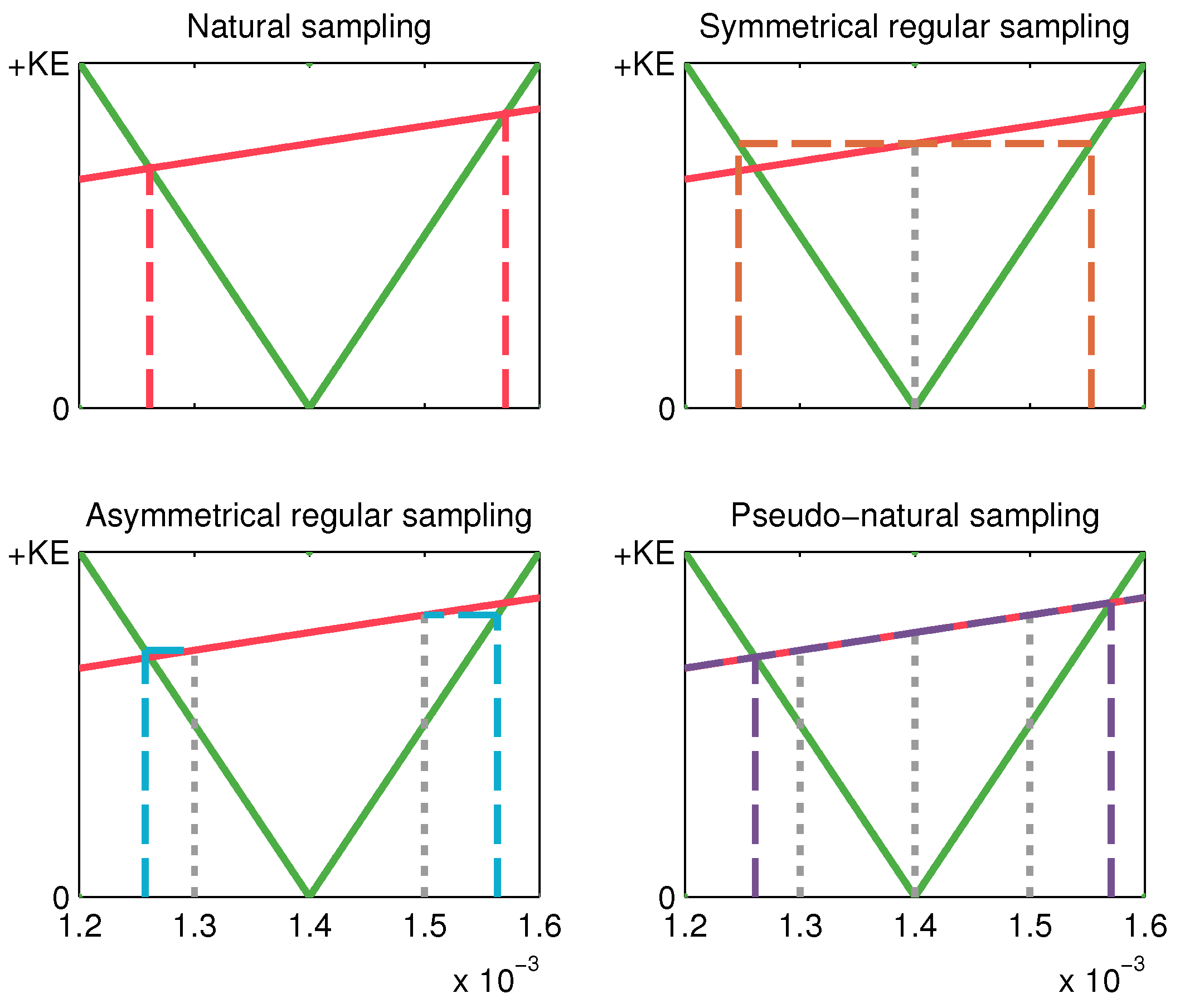
Figure 4.
Sampling methods for a given switching interval: Comparison of natural, symmetrical regular, asymmetrical regular, and pseudo-natural sampling methods for SPWM.
Figure 4.
Sampling methods for a given switching interval: Comparison of natural, symmetrical regular, asymmetrical regular, and pseudo-natural sampling methods for SPWM.
Figure 5.
Switching interval and switching instants yield by four sampling techniques corresponds with the square shown in
Table 2 for case (a).
Figure 5.
Switching interval and switching instants yield by four sampling techniques corresponds with the square shown in
Table 2 for case (a).
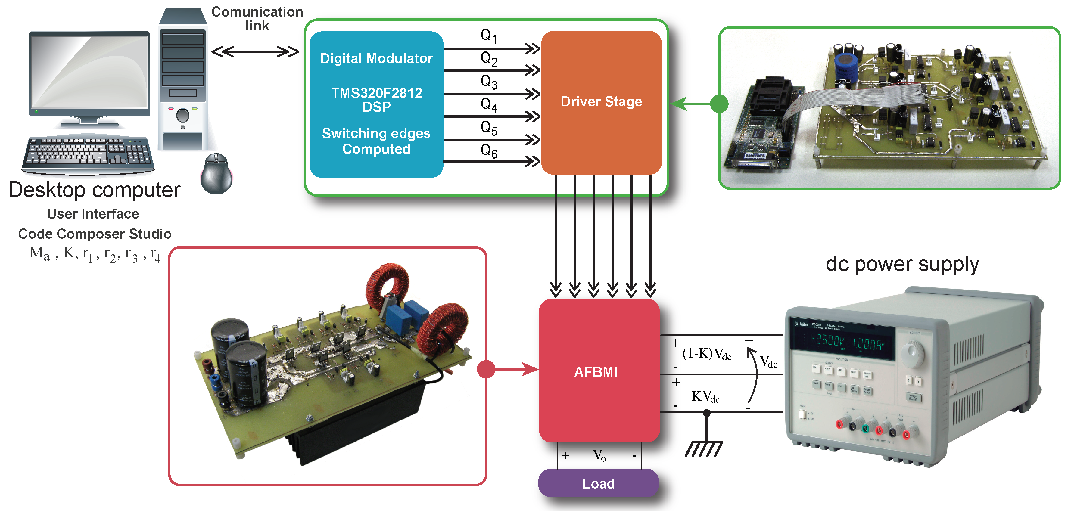
Figure 6.
Block diagrams of the open loop system prototype.
Figure 6.
Block diagrams of the open loop system prototype.
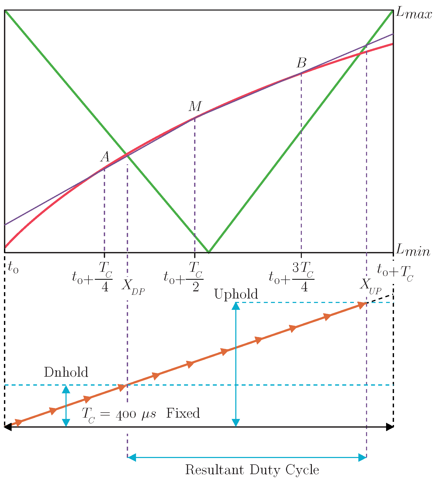
Figure 7.
Generation of switching edges and .
Figure 7.
Generation of switching edges and .
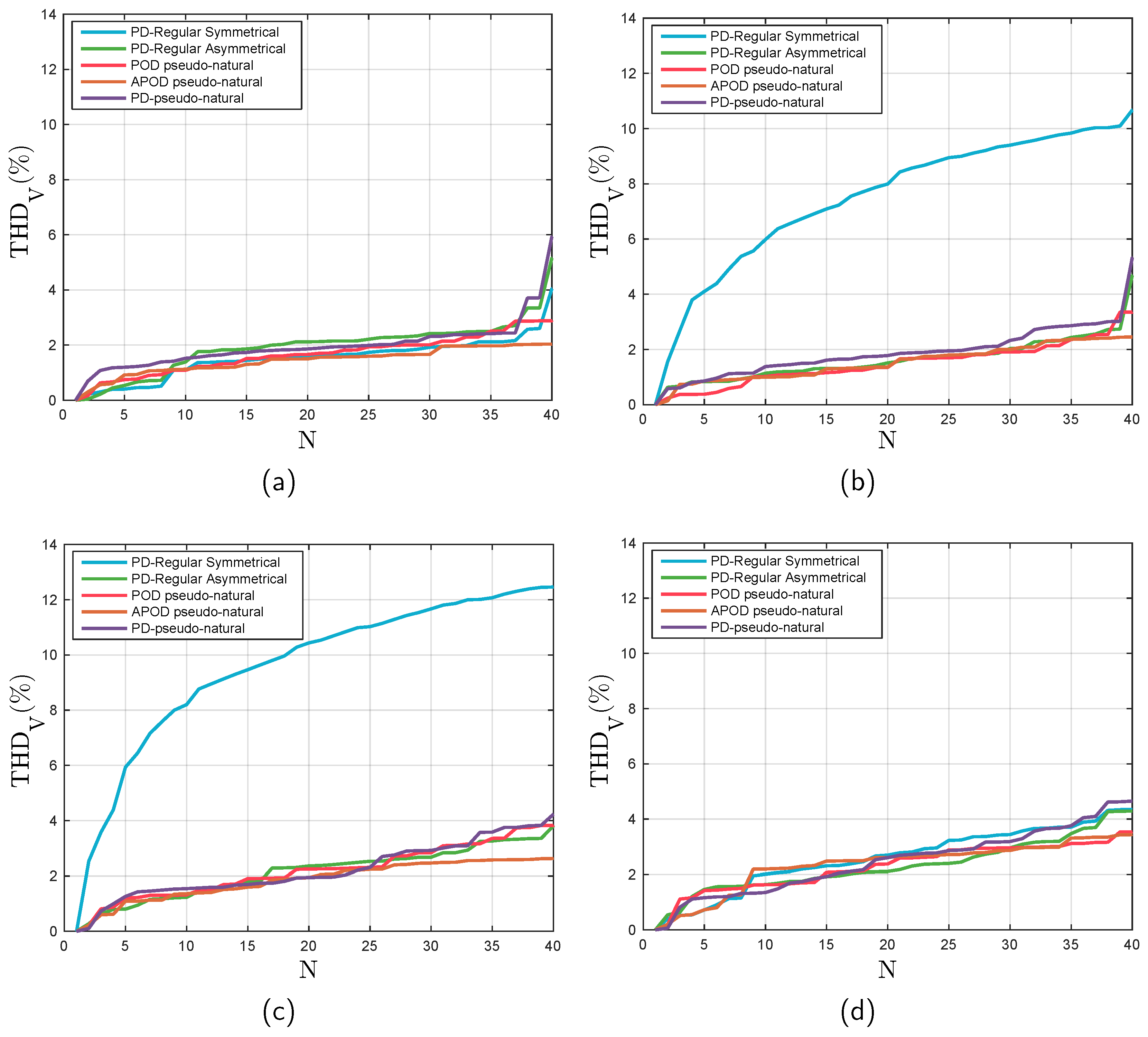
Figure 8.
of PD, POD, and APOD with pseudo-natural sampling and of PD with regular symmetrical and asymmetrical sampling with level distribution , , and modulation index Ma: (a) 0.9, (b) 0.8, (c) 0.7, and (d) 0.6.
Figure 8.
of PD, POD, and APOD with pseudo-natural sampling and of PD with regular symmetrical and asymmetrical sampling with level distribution , , and modulation index Ma: (a) 0.9, (b) 0.8, (c) 0.7, and (d) 0.6.
Table 1.
Comparison of sampling methods when the modulator is within the angle . , , and . Switching instants are obtained from MATLAB and Pspice simulations.
Table 1.
Comparison of sampling methods when the modulator is within the angle . , , and . Switching instants are obtained from MATLAB and Pspice simulations.
| Switching Time | Natural Sampling | Pseudo-Natural Sampling | Symmetrical Regular Sampling | Asymmetrical Regular Sampling |
|---|
| Value | Percent Error | Value | Percent Error | Value | Percent Error |
|---|
| 179.74 s | 179.7 s | 0.022% | 177.43 s | 1.29% | 188.73 s | 5.00% |
| 225.54 s | 225.48 s | 0.027% | 222.66 s | 1.28% | 233.93 s | 3.72% |
| 45.8 s | 45.78 s | 0.044% | 45.23 s | 1.25% | 45.2 s | 1.31% |
Table 2.
Comparison of sampling methods in the time and frequency domains with V, , , , and for (a) PD-SPWM, (b) POD-SPWM, and (c) APOD-SPWM.
Table 3.
Comparison of sampling methods in the time and frequency domains: Regular symmetrical, regular asymmetrical, and pseudo-natural against natural sampling with PD-SPWM, V, , , and for (a) , (b) , and (c) .
Table 4.
Comparison of sampling methods in the time and frequency domains: Regular symmetrical, regular asymmetrical, and pseudo-natural against natural sampling with PD-SPWM, V, , , and for (a) , (b) , and (c) .
Table 5.
Switching states and voltage levels.
Table 5.
Switching states and voltage levels.
| State | Level | | | | | | | | |
|---|
| E | 1 | 1 | X | 0 | 0 | 1 | 0 | 0 |
| | 0 | 1 | 1 | 0 | 0 | 1 | 1 | 1 |
| 0 | 0 | 0 | 1 | 1 | 0 | 1 | 0 | 0 |
| 0 | 1 | 1 | 0 | 0 | 1 | 0 | 0 | 0 |
| | 0 | 1 | 1 | 0 | 1 | 0 | 1 | 1 |
| | 0 | X | 1 | 1 | 1 | 0 | 0 | 0 |
Table 6.
Pseudo-natural against natural sampling with PD-SPWM, V, , and for (a) and ; (b) and ; abd (c) , , , , and .


