1. Introduction
Crystalline silicon heterojunction (SHJ) solar cells have attracted significant attention in recent years, as they can provide high performance together with the prospect of low-cost fabrication and a decrease of silicon wafer thickness below 100 µm [
1]. The advantage of the heterojunction between amorphous and crystalline silicon was first introduced into the so-called HIT concept (Hetero-junction with Intrinsic Thin-layer) by the former company SANYO (Osaka, Japan) (currently part of the company Panasonic) in 1992 [
2]. The SHJ HIT solar cell is composed of a single thin crystalline silicon wafer surrounded by ultra-thin intrinsic amorphous silicon (a-Si:H) and n-type and p-type doped a-Si:H layers, which can be deposited at temperatures below 200 °C and thus can be used in the processing of thin wafers. On the two doped layers, transparent conducting oxide (TCO) layers and metal electrodes are formed with sputtering and screen-printing methods, respectively. The TCO layer on the top also works as an anti-reflection layer.
One of the key technologies of the SHJ solar cells is the interface defect density between the silicon wafer and a-Si:H layers. For n-type crystalline silicon-based SHJ, the p-type a-Si:H is used as an emitter, and it is well-known that the doped a-Si:H layers contain a significantly high defect density. The interface defects between the wafer and the doped a-Si:H is high, and thus a very thin intrinsic a-Si:H is required to be inserted at the interface. Considerable efforts have been made to reduce the carrier recombination rate at the a-Si:H/c-Si interface [
3,
4,
5,
6]. Due to the higher band gap of a-Si:H (about 1.7 eV) compared to that of c-Si, a carrier-selective emitter can be formed, which repels electrons by using a high barrier presented in the conduction band, while the holes can tunnel through the interface to the p-type a-Si:H emitter [
7]. Typically, in n-type SHJ solar cells, the band mismatch is about 0.15–0.2 eV for the conduction band, and is about 0.45 eV for the valence band. The p-type emitter is also important for SHJ solar cells, which should have a low absorption coefficient as the light absorbed in this emitter would not contribute to the device current due to the high defects in the doped a-Si:H [
8]. The emitter requires high conductivity in order to decrease the series resistance (R
s) and to increase the carrier collection. There is increasing interest in developing various materials to replace a-Si:H emitters, such as nanocrytalline silicon [
9] to increase conductivity and silicon carbide [
10,
11] to increase the band gap.
In this study, p-type amorphous silicon oxide (a-SiOx) films are prepared using inductively-coupled plasma chemical vapor deposition (ICPCVD). The a-SiOx:H thin films having low light absorption, a wide band gap, and high conductivity are suitable for the use as a window layer of the SHJ solar cells. The objective of this work is to deposit a-SiOx:H films with different band gaps and conductivity by varying the carbon dioxide (CO2) gas flow rate and to investigate their effects on SHJ solar cell performance.
2. Materials and Methods
Boron-doped a-SiO
x films were deposited using a 13.56 MHz ICPCVD system using a gas mixture of B
2H
6, SiH
4 and CO
2. The substrate temperature was kept at 200 °C. The CO
2 gas flow rate was varied from 2 to 10 standard cubic centimeters per minute (sccm). The power density was 0.03 W/cm
2. Detailed deposition parameters are summarized in
Table 1. The films were deposited on flat glass substrates for optical, electrical, and structural characterization. The band gap (
Eg) of the films was obtained by using a Tauc plot using the following equation [
12]:
where
α is the absorption coefficient determined from transmission and reflection spectra measured by a UV-visible spectrometer,
hv is the photon energy,
n is 1/2 for direct band gap materials or 2 for indirect band gap materials, and
A is the band tailing parameter. The plotting of (
αhυ)^(1/
n) versus
hυ gives a straight line in a certain region. The extrapolation of this straight line intercepts the (
hυ)-axis to give
Eg. The atomic ratio of oxygen to silicon of the a-SiO
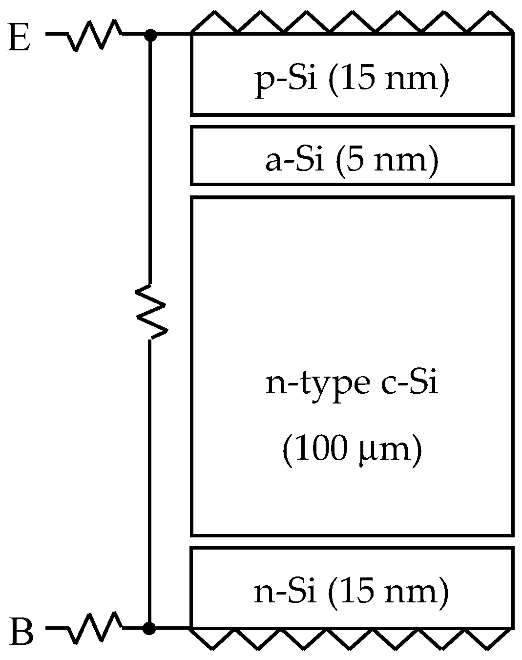
x films was measured by using X-ray photoelectron spectroscopy (XPS). The conductivity of the films was measured in a perpendicular direction of the films. PC1D simulation software (version 5.9, University of New South Wales, Sydney, Australia) was used. The device structure was p-type a-SiO
x (15 nm)/intrinsic a-Si:H (5 nm)/n-type c-Si (100 μm)/n-type a-Si:H (15 nm). The front and rear textured surfaces, with depths of 3 μm and angles of 54.74°, were applied. The device scheme is shown in
Figure 1. The minimum set of the simulation parameters is summarized in
Table 2, where
Na is acceptor concentration,
Nd is donor concentration,
μn is electron mobility,
μp is hole mobility, and
Seff is the surface recombination rate.
3. Results
Figure 2 shows the O/Si atomic ratio and band gap of the a-SiO
x films deposited at a different CO
2 flow rate. It can be seen that the O/Si ratio is about 14.7% at the CO
2 flow rate of 2 sccm. The ratio increases by increasing the CO
2 flow rate. The ratio reaches 44% when the flow rate increases to 10 sccm. This result indicates that the oxygen content in the films increases when the flow rate increases. For a typical a-Si:H film deposited by plasma chemical vapor deposition, the band gap of the films is about 1.6–1.7 eV depending on hydrogen incorporation [
13]. The low CO
2 gas flow rate of 2 sccm leads to an O/Si ratio of 14.7%, and this oxygen incorporation increased the band gap of the film to 1.78 eV, which is slightly higher than a-Si:H films (about 1.7 eV). At a CO
2 flow rate of 6 sccm, the film with O/Si ratio of 34.3% corresponds to a band gap of 1.95 eV. Further increasing the flow rate to 10 sccm, or O/Si ratio up to 44.1%, gives a band gap of 2.1 eV. When a higher band gap material is used for an emitter of n-type SHJ solar cells, the mismatch at the conduction band and valence band could help formation of a selective contact. When a wider band gap p-type material is in contact with n-type c-Si, the band at the interface of the c-Si side will bend downward. The Fermi-level at the interface region is, then, much closer to the valence band compared to the conduction band, and this forms a minority carrier inversion layer that could significantly lower the interface recombination rate and eventually enhance the open-circuit voltage (
Voc) [
14]. Furthermore, the
Voc of an n-type SHJ can be expressed as [
15]:
where
φB is the effective barrier height for recombination,
A is the ideality factor,
q is the electron charge, k is the Boltzmann constant,
T is the absolute temperature,
Nc is the effective densities of state of the conduction band,
Sn is the surface recombination rate for electrons, and
Jsc is the short-circuit current density. The
φB is the distance from the Fermi level to conduction band at the interface. Thus, a higher band gap emitter could in turn have more band bending that increases
φB and eventually
Voc. The a-SiO
x films with the highest band gap of 2.1 eV are expected to have a higher
Voc among others. In addition, the high band gap will also allow more incident light to enter the device, and this may enhance
Jsc.
Figure 3 shows the perpendicular conductivity of the a-SiO
x films deposited at a different CO
2 gas flow rate. It can be seen that the conductivity reduces from 4.1 to 2.5 S/cm when the CO
2 flow rate increases from 2 to 10 sccm. The increase of the oxygen content in the films reduces the conductivity. The O/Si ratio of the films increases as the CO
2 flow rate increases. The film structure would be relatively close to SiO
2, and thus the conductivity would decrease. The overall series resistance of SHJ devices should be the sum of the resistances of indium tin oxide (ITO), the p-type emitter, the n-type c-Si, and the n-type a-Si:H (resistances of metal contacts are neglected). The perpendicular conductivity of the p-type emitter can be used as an indicator to evaluate the series resistance contributed by the p-type emitter. The lower oxygen content films have a high conductivity, and thus are expected to have a low series resistance and, ultimately, a higher fill factor (FF). Therefore, there is a tradeoff between the gain in
Voc brought by the increased band gap and the loss in FF due to the decreased conductivity at an increasing CO
2 flow rate.
To determine the best film for the p-type emitter among the a-SiO
x films with different CO
2 flow rates, the properties of the films are input into simulation software. The absorption coefficient spectra of the films were analyzed using the transmittance spectra. The reflectance spectra are input according to the measured data for the structure of ITO/p-type a-SiO
x/intrinsic a-Si:H/n-type c-S/n-type a-Si:H structure, where the ITO was deposited using a DC magnetron sputter system. We prepared an intrinsic a-Si:H thin film by plasma enhanced chemical vapor deposition using H
2 and SiH
4 on the both sides of c-Si. The intrinsic a-Si:H layer had a hydrogen content of about 10% and a band gap of 1.7 eV. The measured minority carrier lifetime (using Sinton WCT120) was 344 μs, corresponding to a surface recombination rate of 0.15 cm/s. In the simulation, by assuming the ideal passivation of the intrinsic a-Si:H on c-Si for simplification, the surface recombination rate of the c-Si interface is not considered. The deposition of different p-type a-SiO
x:H layers might not change the i-layer properties, and thus the hydrogen and oxygen in the p-layer would not significantly affect the c-Si surface’s passivation quality. Therefore, the simulation may present an overestimated result, but the trend and influence of the p-type emitter layers on device performance are still validated.
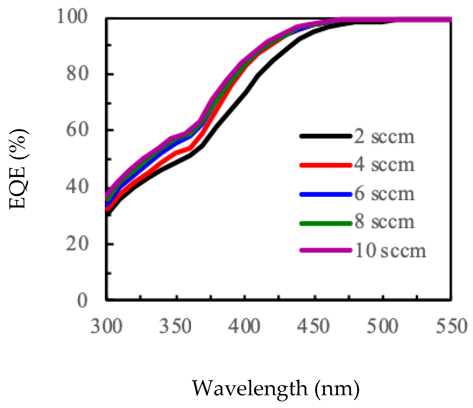
Figure 4 shows the external quantum efficiency (EQE) in a wavelength range of 300–550 nm for SHJ solar cells with different p-type emitters. The difference between the curves with wavelengths higher than 550 nm is neglected, so the spectral response in the long wavelength region is not shown. It is also noted that as the light is incident from the p-type emitter side, the impact of the emitter is mainly at the short-wavelengths. It can be seen that the EQE response increases with increasing the CO
2 flow rate. This enhancement is mainly explained by the increased band gap and accordingly reduced absorption of the light in the emitter region. Note that the light absorbed in the emitter would not contribute to the device current. The relationship between
Jsc and EQE is given by
where
h is the Planck constant,
λ is the wavelength, and
P(
λ) is the sun spectra at the AM1.5G condition. Therefore, a higher EQE response gives a higher
Jsc. This evidences the expectation that higher band gap emitter can improve the
Jsc of the device. It is noted that when the CO
2 flow rate is greater than 6 sccm, corresponding to a band gap of 1.95 eV, the EQE curves are similar. This might indicate that light absorption in emitter is already too low to gain further improvement.
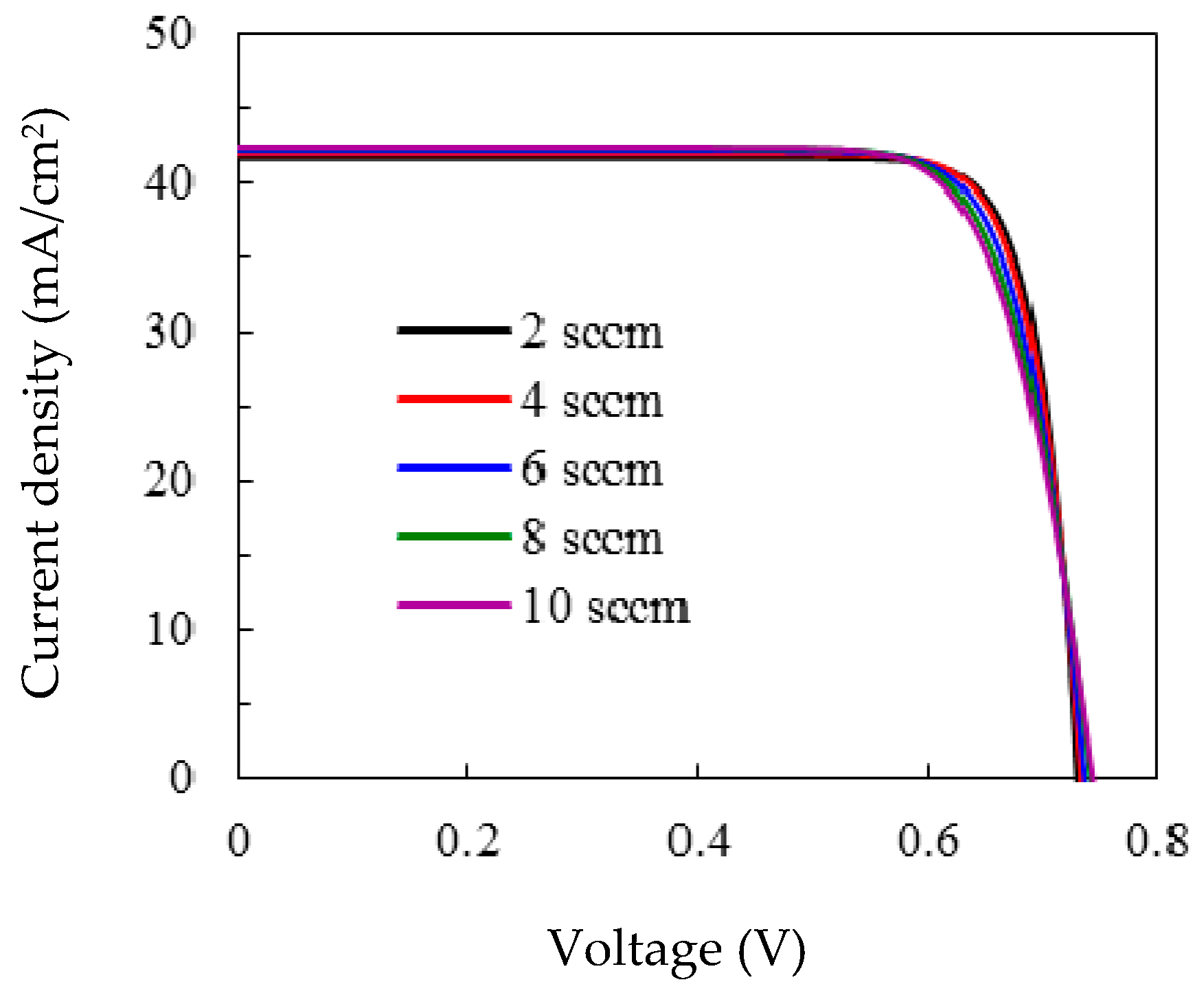
The simulated current density-voltage (J-V) curves of the SHJ solar cells with different p-type emitters are shown in
Figure 5. The extracted photovoltaic external parameters, such as
Voc,
Jsc, FF and conversion efficiency (
η), are listed in
Table 3. It can be seen that the
Jsc increases from 41.63 to 42.31 mA/cm
2 when the CO
2 flow rate increases from 2 to 8 sccm. The FF, on the other hand, reduces from 0.825 to 0.785 after increasing the CO
2 flow rate from 2 to 8 sccm. It is noted that one main factor affecting the solar cell’s FF is R
s, which is related to the conductivity in each layer, carrier transport through the junction, and the contact resistivity of the TCO/p-layer/i-layer stack to c-Si. The carrier transport is influenced by i and p layer thickness, their band gap, the activation energy of doped layer, and work function of the TCO layer [
16]. In this simulation, the TCO layer is not considered. The front and rear electrodes are assumed to be perfectly conductive and transparent. The contact resistivity of the TCO/p-layer/i-layer stack to c-Si is also not considered. The total R
s is, therefore, mainly influenced by p-layer conductivity. The case of 10 sccm shows a nearly 5% drop in FF compared to the case of 2 sccm. The reduction in FF is mainly attributed to the decreased p-layer conductivity due to the increase in the oxygen content of the emitter layer. In contrast,
Jsc increases by 1.6%, which is much lower than the drop of FF. The
Voc increases from 730 to 745 mV when the CO
2 flow rate increases from 2 to 8 sccm. The solar cell
Voc might be affected by Si surface passivation and the band bending at the a-Si/c-Si interfaces. The latter is related to the band gap, activation energy, and work function of TCO layer. The TCO layer is not considered in the simulation. The activation energies of the p-layers deposited at the CO
2 flow rate of 2, 4, 6, 8, and 10 sccm are 52, 54, 58, 67, and 73 meV, respectively. Overall, the value of
η increase from 25.07% to 25.58% by increasing the CO
2 flow rate from 2 to 6 sccm, and further increasing the flow rate from 6 to 10 sccm leads to a reduction in
η from 25.58% to 24.74%. From this result, it can be seen that the gain in
Jsc and
Voc due to using a large band gap emitter will possibly be offset by the loss in FF. The emitter properties should, therefore, be carefully controlled. In the present study, solar cells featuring an a-SiO
x emitter with a band gap of 1.95 eV have the best
η.


