Development and 24 Hour Behavior Analysis of a Peak-Shaving Equipment with Battery Storage

 ,
,  ,
,  ,
, 
Abstract
1. Introduction
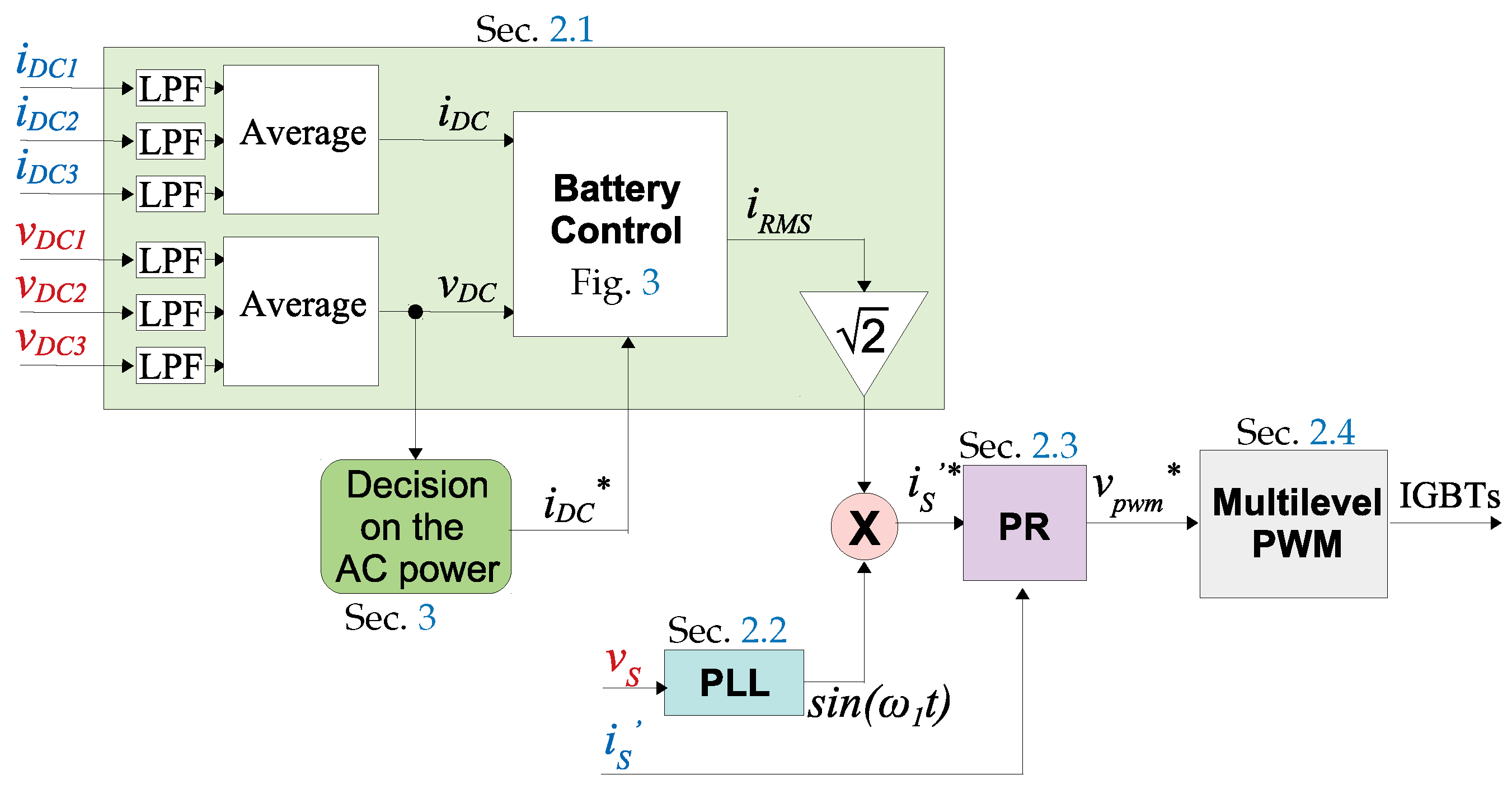
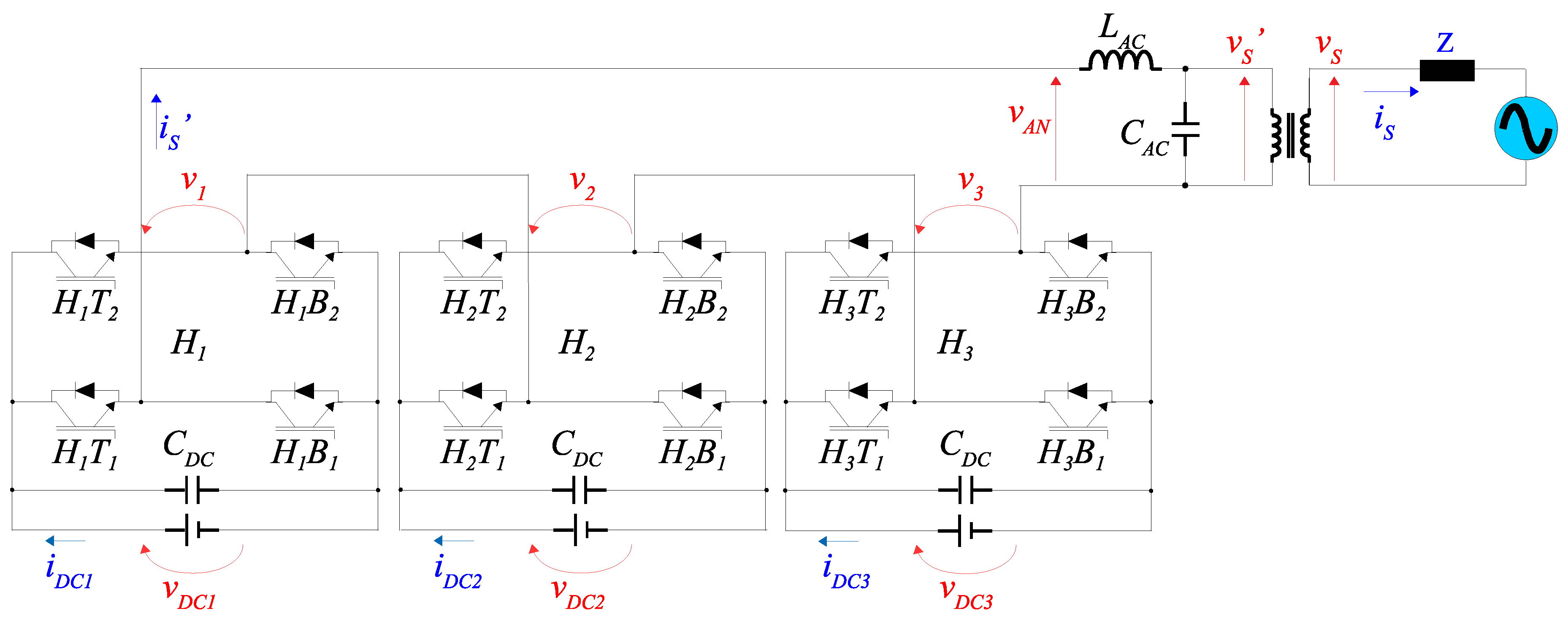
2. Developed Equipment for Peak-Shaving
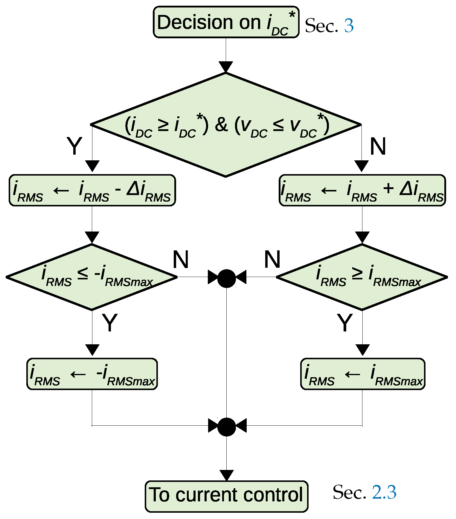
2.1. Batteries Charge and Discharge Control
- Stage I: The battery voltage (where x indicates the bridge number) increases gradually, while a constant current is imposed by the controller;
- Stage II: The battery voltage is kept constant by the controller, while its current drops to near zero;
- Stage III: The battery voltage is kept constant by the controller, while a minimum current is drawn only to maintain the charge. At this stage, the battery is already fully charged and is said to be ”floating”.
2.2. Phase Locked Loop
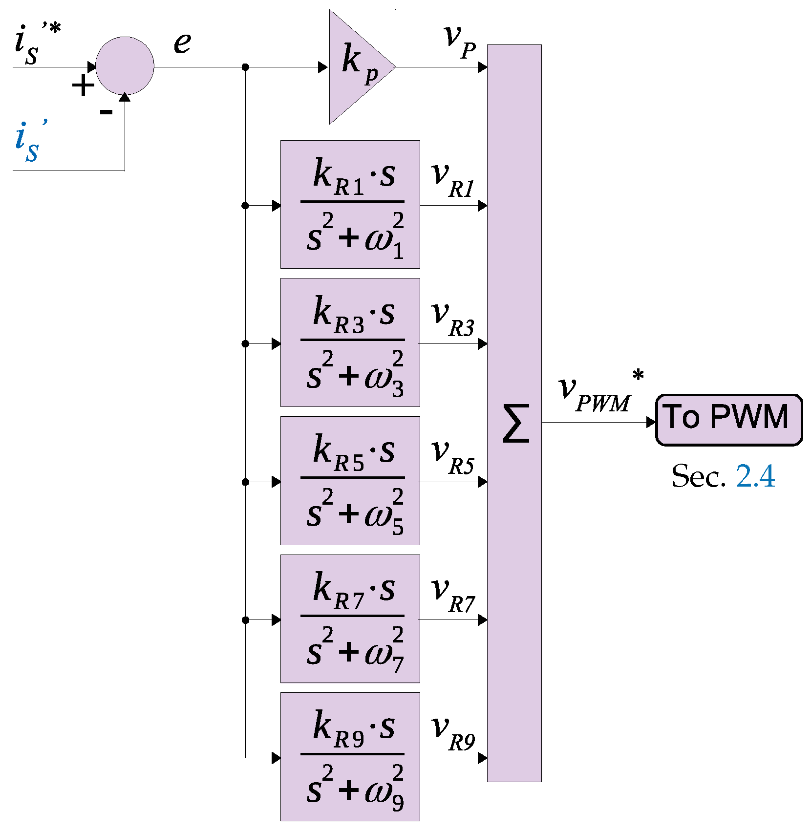
2.3. AC Control Loop
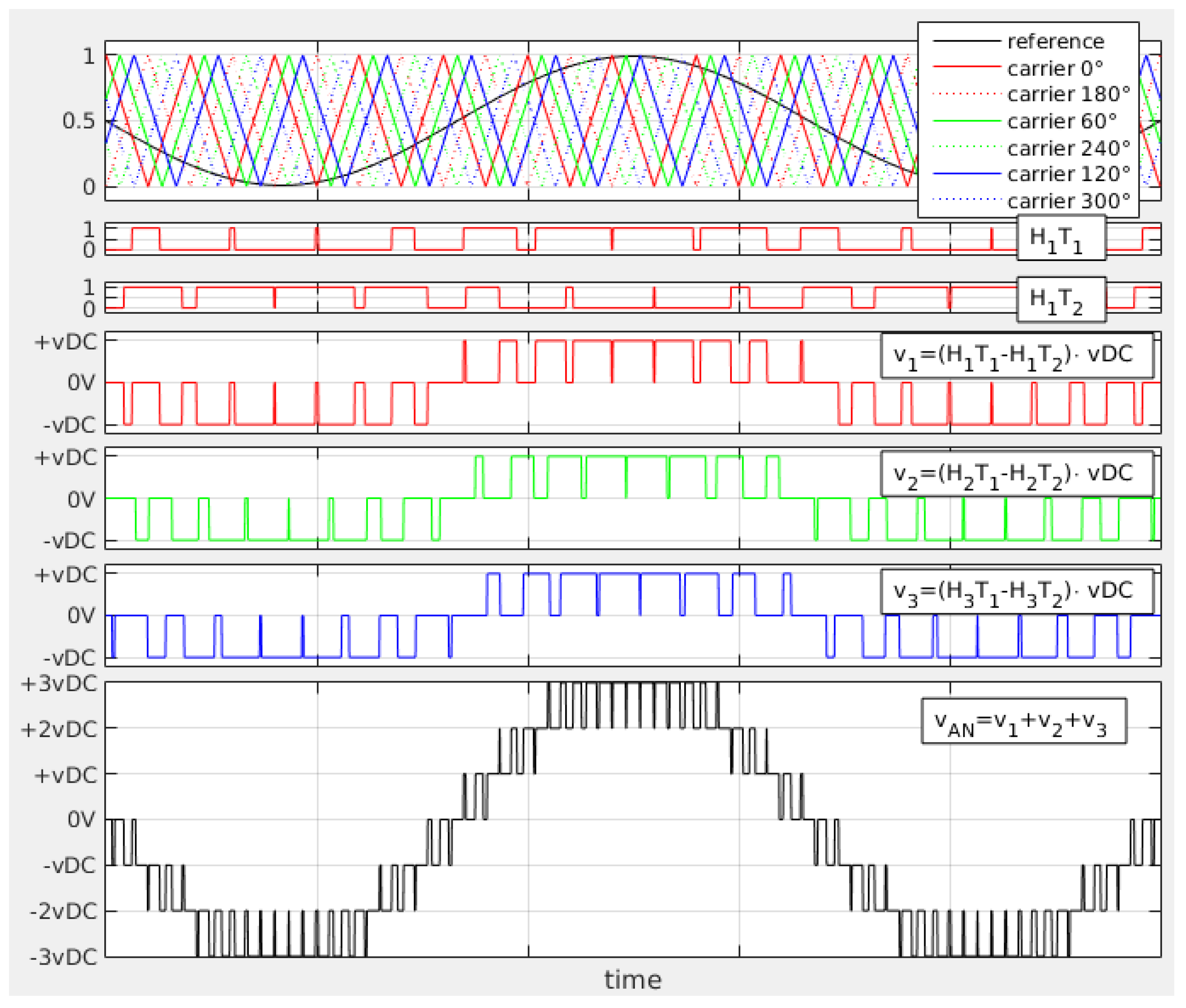
2.4. Multilevel Pulse Width Modulation
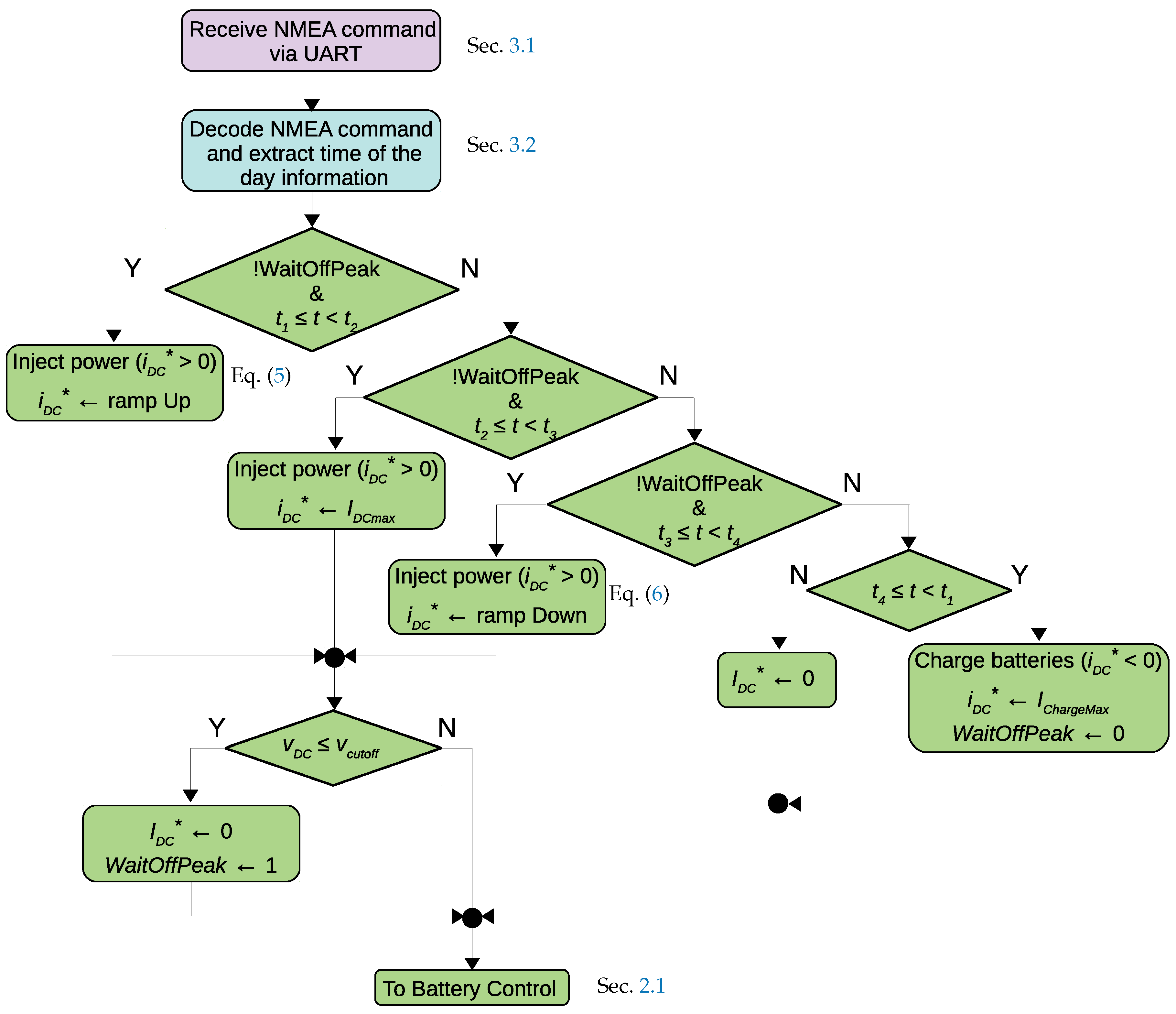
3. Decision on the AC Power
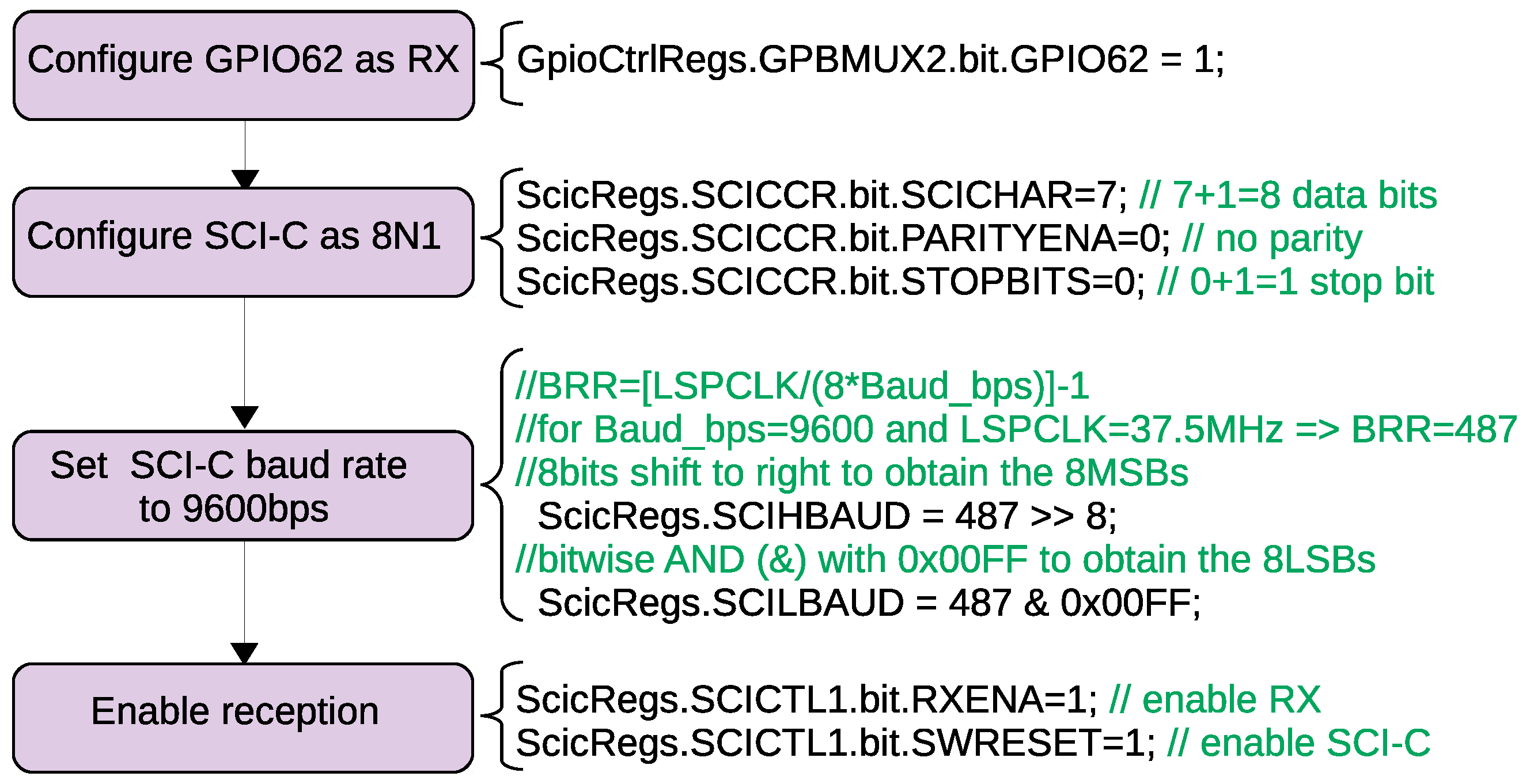
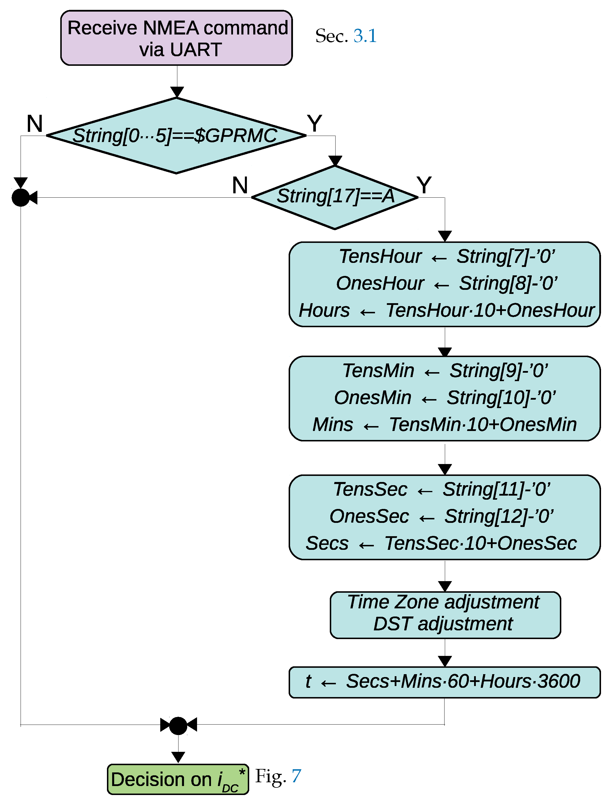
3.1. UART Serial Communication between the Adafruit GPS Module and the TMS320F28335 DSP
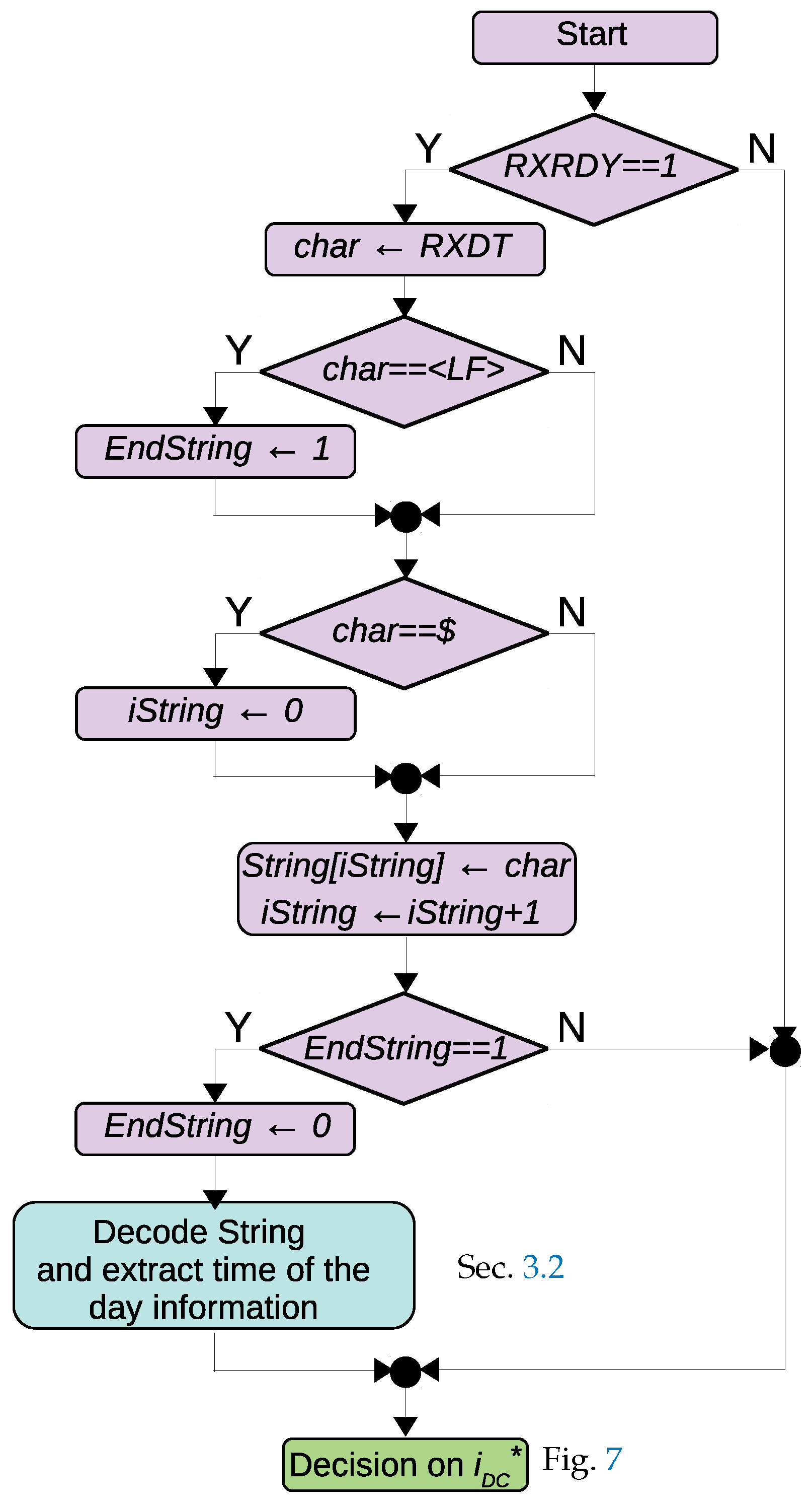
3.2. Decoding of GPS Commands
4. Experimental Setup
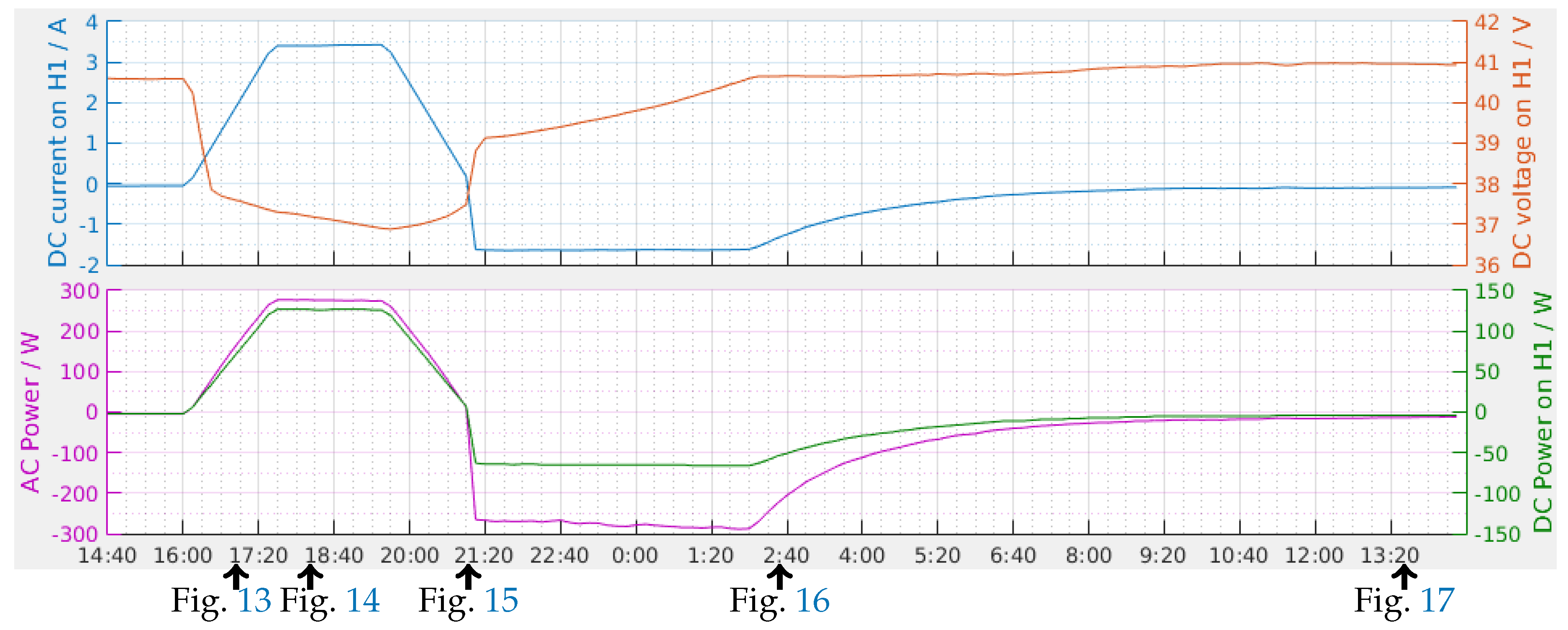
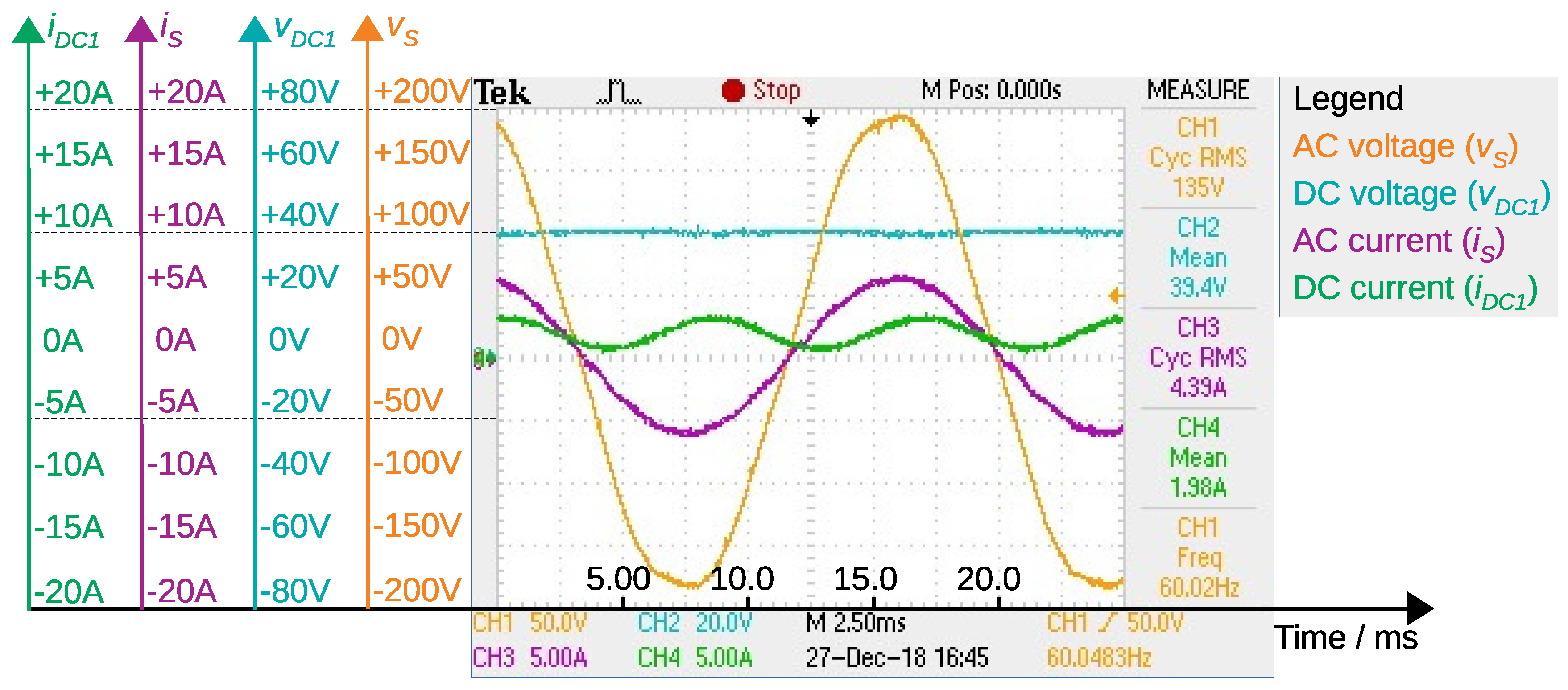
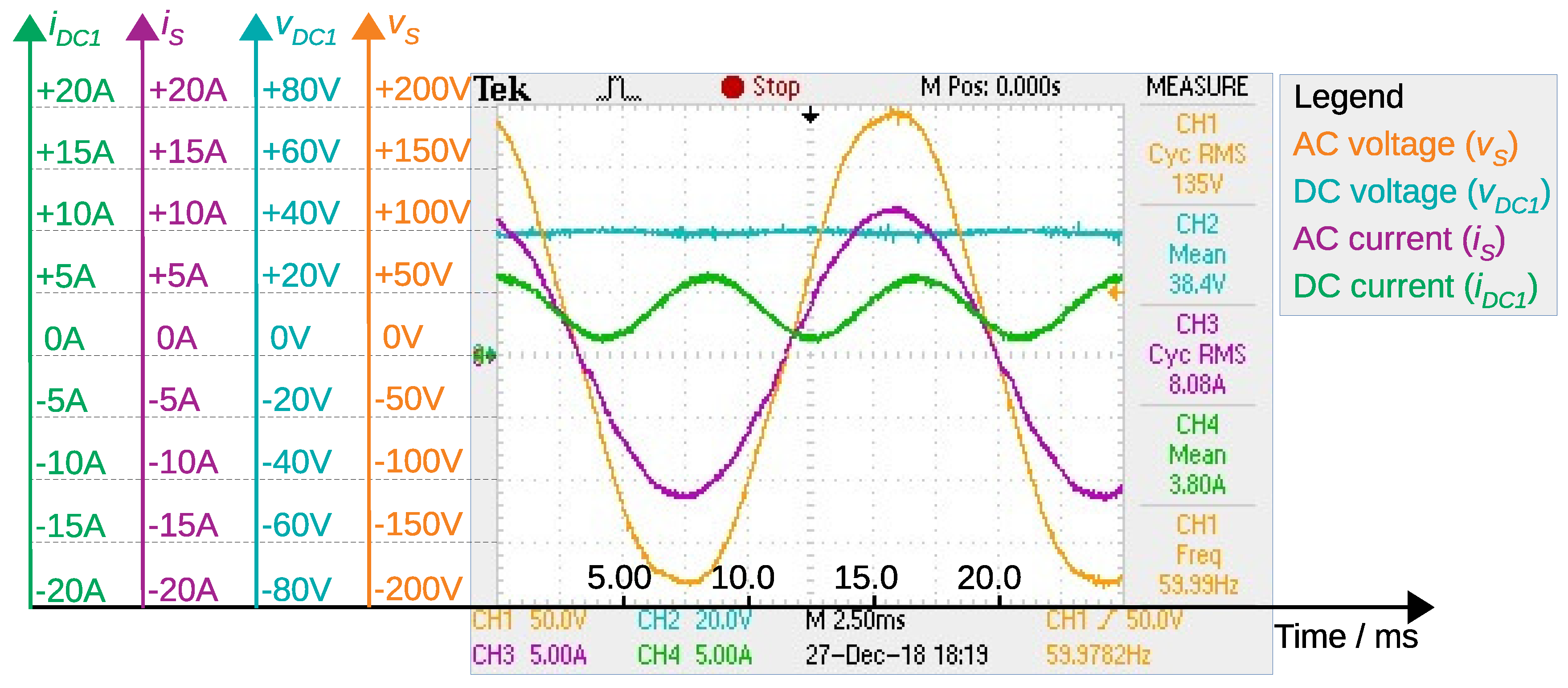
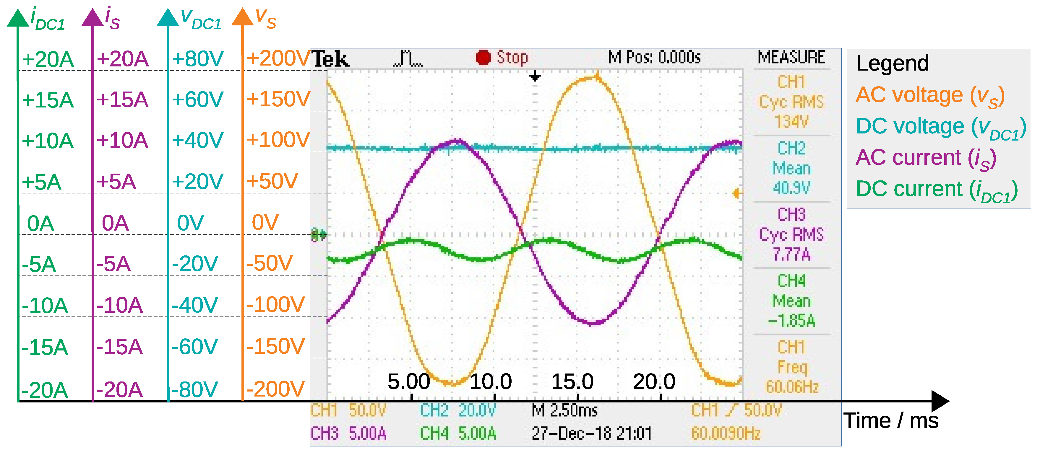
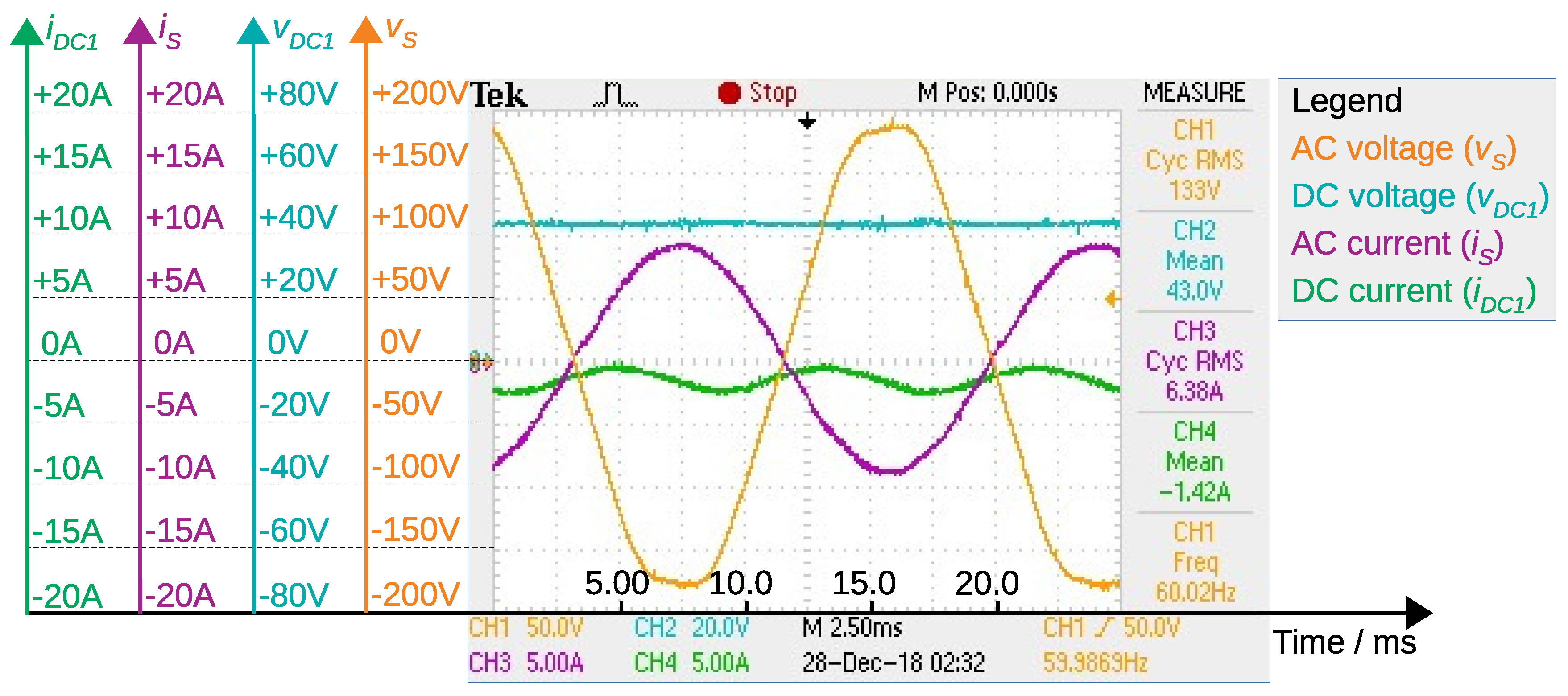
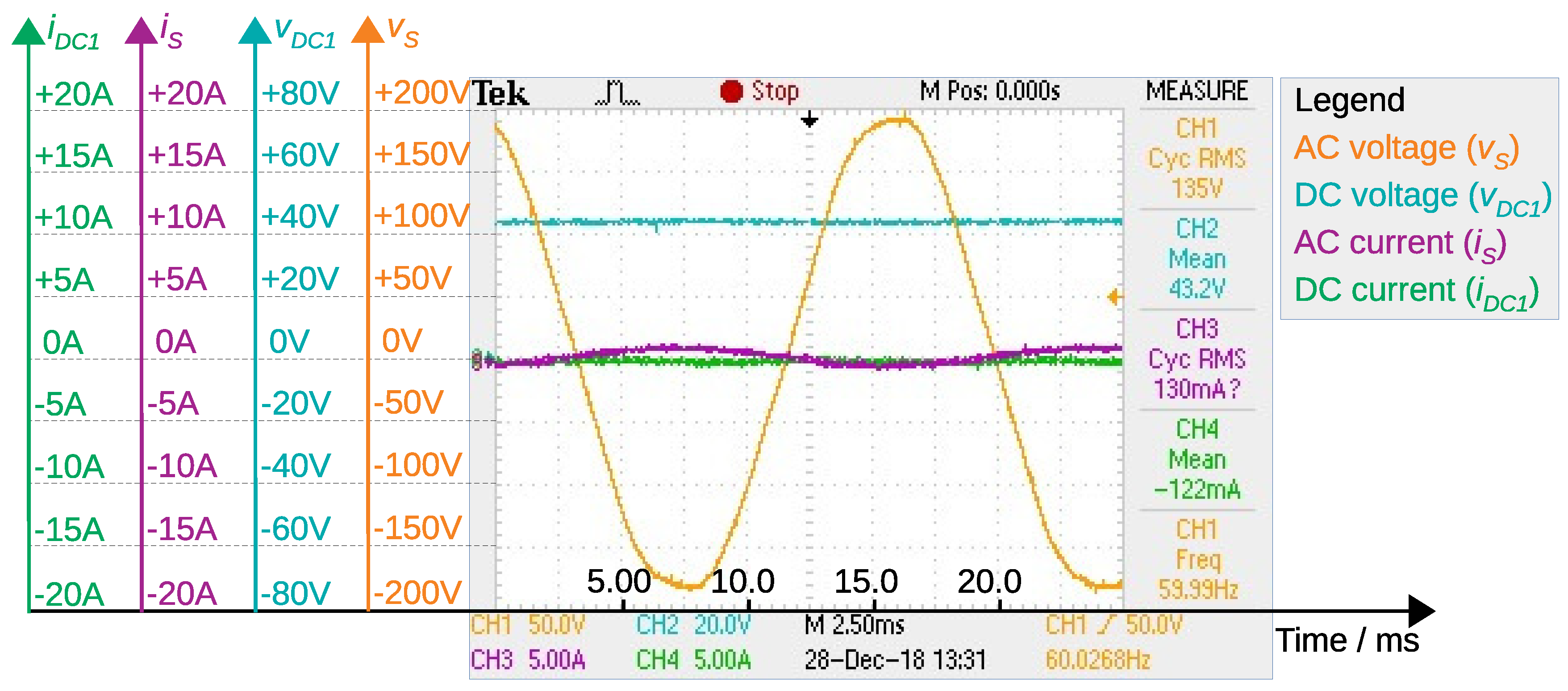
5. Experimental Results
6. Conclusions
Author Contributions
Acknowledgments
Conflicts of Interest
Abbreviations
| ASCII | American Standard Code for Information Interchange |
| CAES | Compressed Air Energy Storage |
| DSP | Digital Signal Processor |
| DST | Daylight Saving Time |
| GPS | Global Positioning System |
| IGBT | Insulated Gate Bipolar Transistor |
| LPF | Low Pass Filter |
| NMEA | National Marine Electronics Association |
| PHS | Pumped Hydroelectric Storage |
| PI | Proportional Integral controller |
| PLL | Phase Locked Loop |
| PR | Proportional plus Resonant controller |
| PWM | Pulse Width Modulation |
| RTC | Real Time Clock |
| SCI | Serial Communication Interface |
| SMES | Superconducting Magnetic Energy Storage |
| UART | Universal Asynchronous Receiver-Transmitter |
| UTC | Coordinated Universal Time |
List of Symbols
| Step size of AC current reference | A | |
| Maximum number of samples allowed for PLL phase error | - | |
| PLL phase error | rad | |
| Resonant frequency of PR controller of harmonic order h | rad/s | |
| , , | Autoregressive coefficients of discretized resonant transfer functions of order h | - |
| A | Nominal amplitude of utility voltage | V |
| Input coefficients of discretized resonant transfer functions of order h | - | |
| AC filter capacitor | F | |
| DC capacitors at each H-bridge | F | |
| e | PR controller current error | A |
| Nominal frequency of utility voltage | Hz | |
| Sampling frequency | Hz | |
| i | PLL look-up table pointer | - |
| Maximum DC current at battery charge | A | |
| DC currents on battery banks 1, 2 and 3 | A | |
| Averaged DC current of the battery banks | A | |
| DC current reference of the battery banks | A | |
| Maximum DC current at battery discharge | A | |
| RMS value of AC current reference | A | |
| Maximum RMS value of AC current reference | A | |
| AC current at utility side of the transformer | A | |
| AC current at converter side of the transformer | A | |
| AC current reference for PR controller | A | |
| Proportional gain of PR controller | V/A | |
| Resonant gain of PR controller of harmonic order h | V/A | |
| Gain for conversion of PLL phase error to number of samples | 1/rad | |
| AC filter inductor | H | |
| PLL phase error converted to number of samples | - | |
| Oscillating component of PLL quadrature signal | V | |
| Constant component of PLL quadrature signal | V | |
| t | Time of the day | s |
| Start time of ramp-up current injection | s | |
| Start time of maximum current injection | s | |
| End time of maximum current injection | s | |
| End time of ramp-down current injection | s | |
| Sampling period | s | |
| Individual output voltages of H bridges | V | |
| Composed multilevel output voltage | V | |
| Cut-off voltage of battery banks | V | |
| DC voltages at battery banks 1, 2 and 3 | V | |
| Averaged DC voltage of the battery banks | V | |
| DC floating voltage reference of the battery banks | V | |
| Output of PR controller | V | |
| Output of resonant transfer function of harmonic order h | V | |
| AC voltage at utility side of the transformer | V | |
| AC voltage at converter side of the transformer | V |
References
- Strbac, G. Demand side management: Benefits and challenges. Energy Policy 2008, 36, 4419–4426. [Google Scholar] [CrossRef]
- Lai, C.S.; Jia, Y.; Lai, L.L.; Xu, Z.; McCulloch, M.D.; Wong, K.P. A comprehensive review on large-scale photovoltaic system with applications of electrical energy storage. Renew. Sustain. Energy Rev. 2017, 78, 439–451. [Google Scholar] [CrossRef]
- Hesse, H.C.; Schimpe, M.; Kucevic, D.; Jossen, A. Lithium-Ion Battery Storage for the Grid—A Review of Stationary Battery Storage System Design Tailored for Applications in Modern Power Grids. Energies 2017, 10, 2107. [Google Scholar] [CrossRef]
- Boicea, V.A. Energy Storage Technologies: The Past and the Present. Proc. IEEE 2014, 102, 1777–1794. [Google Scholar] [CrossRef]
- Akinyele, D.; Belikov, J.; Levron, Y. Battery Storage Technologies for Electrical Applications: Impact in Stand-Alone Photovoltaic Systems. Energies 2017, 10, 1760. [Google Scholar] [CrossRef]
- Kharel, S.; Shabani, B. Hydrogen as a Long-Term Large-Scale Energy Storage Solution to Support Renewables. Energies 2018, 11, 2825. [Google Scholar] [CrossRef]
- Rodriguez, A.; Huerta, F.; Bueno, E.J.; Rodriguez, F.J. Analysis and Performance Comparison of Different Power Conditioning Systems for SMES-Based Energy Systems in Wind Turbines. Energies 2013, 6, 1527–1553. [Google Scholar] [CrossRef]
- Piorkowski, P.; Chmielewski, A.; Bogdzinski, K.; Mozaryn, J.; Mydlowski, T. Research on Ultracapacitors in Hybrid Systems: Case Study. Energies 2018, 11, 2551. [Google Scholar] [CrossRef]
- Hedlund, M.; Lundin, J.; De Santiago, J.; Abrahamsson, J.; Bernhoff, H. Flywheel Energy Storage for Automotive Applications. Energies 2015, 8, 10636–10663. [Google Scholar] [CrossRef]
- Pavesi, G.; Cavazzini, G.; Ardizzon, G. Numerical Analysis of the Transient Behaviour of a Variable Speed Pump-Turbine during a Pumping Power Reduction Scenario. Energies 2016, 9, 534. [Google Scholar] [CrossRef]
- Wang, J.; Lu, K.; Ma, L.; Wang, J.; Dooner, M.; Miao, S.; Li, J.; Wang, D. Overview of Compressed Air Energy Storage and Technology Development. Energies 2017, 10, 991. [Google Scholar] [CrossRef]
- Rahmann, C.; Mac-Clure, B.; Vittal, V.; Valencia, F. Break-Even Points of Battery Energy Storage Systems for Peak Shaving Applications. Energies 2017, 10, 833. [Google Scholar] [CrossRef]
- Mutarraf, M.U.; Terriche, Y.; Niazi, K.A.K.; Vasquez, J.C.; Guerrero, J.M. Energy Storage Systems for Shipboard Microgrids-A Review. Energies 2018, 11, 3492. [Google Scholar] [CrossRef]
- Vazquez, S.; Lukic, S.M.; Galvan, E.; Franquelo, L.G.; Carrasco, J.M. Energy Storage Systems for Transport and Grid Applications. IEEE Trans. Ind. Electron. 2010, 57, 3881–3895. [Google Scholar] [CrossRef]
- Sant’Ana, W.; Gonzatti, R.; Lambert-Torres, G.; Bonaldi, E.; Pereira, R.; da Silva, L.E.B.; Silva, C.H.; Pinheiro, G.; Mollica, D.; Filho, J.S. Suporte e formação de micro-redes através de conversor multinível. In Proceedings of the Anais do XXII Congresso Brasileiro de Automática—CBA2018, Joao Pessoa, Paraiba, Brazil, 9–12 September 2018. [Google Scholar] [CrossRef]
- TMS320F2833x, TMS320F2823x Digital Signal Controllers (DSCs)—SPRS439N. 2016. Available online: http://www.ti.com (accessed on 20 February 2019).
- Adafruit Ultimate GPS. 2018. Available online: http://www.adafruit.com (accessed on 20 February 2019).
- Sant’Ana, W.C.; Gonzatti, R.B.; Pereira, R.R.; Lambert-Torres, G.; Bonaldi, E.L.; da Silva, L.E.B.; Pinheiro, G.G.; Guimaraes, B.P.B.; da Silva, C.H.; Mollica, D.; et al. Equipamento para corte de picos de demanda baseado em conversor multinível e armazenamento por baterias. In Proceedings of the XVIII Encontro Regional Ibero-americano do Cigré-ERIAC 2019, CIGRÉ-Brasil, Foz do Iguacu, PR, Brazil, 19–23 May 2019. [Google Scholar]
- Da Silva, C.H.; Pereira, R.R.; da Silva, L.E.B.; Lambert-Torres, G.; Bose, B.K.; Ahn, S.U. A Digital PLL Scheme for Three-Phase System Using Modified Synchronous Reference Frame. IEEE Trans. Ind. Electron. 2010, 57, 3814–3821. [Google Scholar] [CrossRef]
- Sant’Ana, W.; Gonzatti, R.; Lambert-Torres, G.; Bonaldi, E.; Pereira, R.; Borges-da Silva, L.E.; Pinheiro, G.; Silva, C.H.; Mollica, D.; Filho, J.S. Implementacao de Funcionalidade de Amortecimento de Propagacao Harmonica em Equipamento de Armazenamento e Suporte de Rede. Revista Eletronica de Potencia 2019. [Google Scholar] [CrossRef]
- Mohan, N.; Undeland, T.M.; Robbins, W.P. Power Electronics—Converters, Applications and Design, 2nd ed.; John Wiley & Sons, Inc.: Hoboken, NJ, USA, 1995. [Google Scholar]
- Wu, B. High-Power Converters and AC Drives; John Wiley & Sons, Inc.: Hoboken, NJ, USA, 2006. [Google Scholar]
- TMS320x2833x, 2823x Enhanced Pulse Width Modulator (ePWM) Module—SPRUG04a. 2009. Available online: http://www.ti.com (accessed on 20 February 2019).
- Sant’Ana, W.; Gonzatti, R.; Guimaraes, B.; Lambert-Torres, G.; Bonaldi, E.; Pereira, R.; da Silva, L.E.B.; Ferreira, C.; de Oliveira, L.; Pinheiro, G.; et al. Development of a multilevel converter for power systems applications based on DSP. In Proceedings of the Simposio Brasileiro de Sistemas Eletricos (SBSE), Niteroi, Brazil, 12–16 May 2018. [Google Scholar] [CrossRef]
- NMEA 0183—Standard for Interfacing Marine Electronic Devices—v.3.01. 2002. Available online: http://www.nmea.org (accessed on 20 February 2019).
- Hammarstron, J.R.; da Rosa Abaide, A.; Blank, B.L.; da Silva, L.N.F. Analysis of the electricity tariffs in Brazil in light of the current behavior of the consumers. In Proceedings of the 2018 53rd International Universities Power Engineering Conference (UPEC), Glasgow, UK, 4–7 September 2018; pp. 1–6. [Google Scholar] [CrossRef]
- TMS320x2833x, 2823x System Control and Interrupts—Reference Guide SPRUFB0D. 2010. Available online: http://www.ti.com (accessed on 20 February 2019).
- TMS320x2833x, 2823x Serial Communications Interface (SCI) SPRUFZ5A. 2009. Available online: http://www.ti.com (accessed on 20 February 2019).


| iString | 0 | 1 | 2 | 3 | 4 | 5 | 6 | 7 | 8 | 9 | 10 | 11 | 12 | 13 | 14 | 15 | 16 | 17 | 18 | … |
| String[] | $ | G | P | R | M | C | , | h | h | m | m | s | s | . | s | s | , | A | , | … |
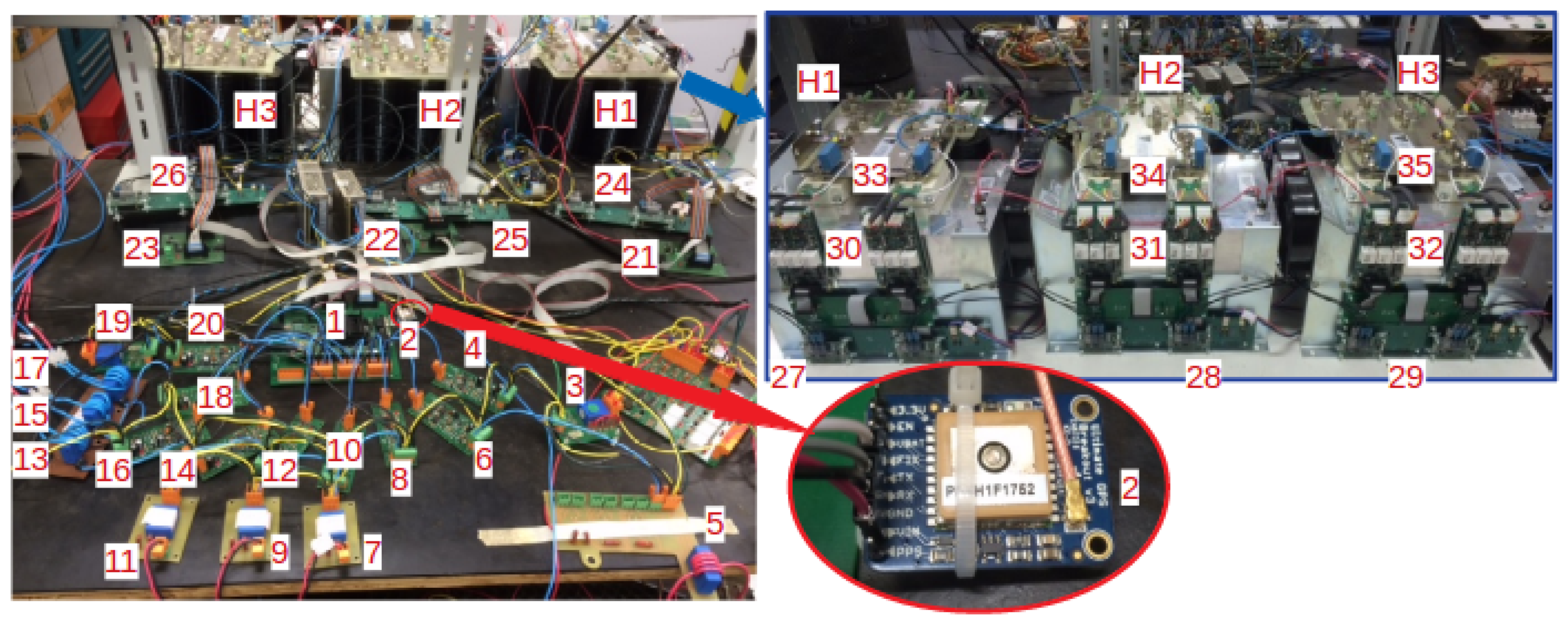
| 1 | TMS320F28335 DSP |
| 2 | Adafruit GPS module |
| 3 | Hall effect sensor |
| 4 | Signal conditioning with OpAmps |
| 5 | Hall effect sensor |
| 6 | Signal conditioning with OpAmps |
| 7, 9, 11 | Hall effect sensor |
| 8, 10, 12 | Signal conditioning with OpAmps |
| 13, 15, 17 | Hall effect sensor |
| 14, 16, 18 | Signal conditioning with OpAmps |
| 19, 20 | Spare boards—not in use |
| 21, 22, 23 | Conversion 3.3V⇔15V |
| 24, 25, 26 | Fiber Optic Transmitters |
| 27, 28, 29 | Fiber Optic Receivers |
| 30, 31, 32 | Gate drivers |
| 33, 34, 35 | IGBT power blocks |
| Source | 127 V (±10%) − 60 Hz |
| Transformer | 127 V/ 440 V − 2.5 kVA |
| Maximum RMS current allowed on | 10 A |
| Filter Inductor | 2.77 mH |
| Filter Capacitor | 10 μF |
| Battery banks (at each H-bridge) | series connection of 3 12V-Lead-Acid-60Ah |
| Battery bank floating voltage reference | 40.5 V |
| Battery bank cut-off voltage | 35 V |
| Maximum DC current injection | +3.8 A |
| Maximum DC current on battery charge | −1.6 A |
© 2019 by the authors. Licensee MDPI, Basel, Switzerland. This article is an open access article distributed under the terms and conditions of the Creative Commons Attribution (CC BY) license (http://creativecommons.org/licenses/by/4.0/).
Share and Cite
Sant’Ana, W.C.; Gonzatti, R.B.; Lambert-Torres, G.; Bonaldi, E.L.; Torres, B.S.; de Oliveira, P.A.; Pereira, R.R.; Borges-da-Silva, L.E.; Mollica, D.; Santana Filho, J. Development and 24 Hour Behavior Analysis of a Peak-Shaving Equipment with Battery Storage. Energies 2019, 12, 2056. https://doi.org/10.3390/en12112056
Sant’Ana WC, Gonzatti RB, Lambert-Torres G, Bonaldi EL, Torres BS, de Oliveira PA, Pereira RR, Borges-da-Silva LE, Mollica D, Santana Filho J. Development and 24 Hour Behavior Analysis of a Peak-Shaving Equipment with Battery Storage. Energies. 2019; 12(11):2056. https://doi.org/10.3390/en12112056
Chicago/Turabian StyleSant’Ana, Wilson Cesar, Robson Bauwelz Gonzatti, Germano Lambert-Torres, Erik Leandro Bonaldi, Bruno Silva Torres, Pedro Andrade de Oliveira, Rondineli Rodrigues Pereira, Luiz Eduardo Borges-da-Silva, Denis Mollica, and Joselino Santana Filho. 2019. "Development and 24 Hour Behavior Analysis of a Peak-Shaving Equipment with Battery Storage" Energies 12, no. 11: 2056. https://doi.org/10.3390/en12112056
APA StyleSant’Ana, W. C., Gonzatti, R. B., Lambert-Torres, G., Bonaldi, E. L., Torres, B. S., de Oliveira, P. A., Pereira, R. R., Borges-da-Silva, L. E., Mollica, D., & Santana Filho, J. (2019). Development and 24 Hour Behavior Analysis of a Peak-Shaving Equipment with Battery Storage. Energies, 12(11), 2056. https://doi.org/10.3390/en12112056