Article

A Modified Step-Up DC-DC Flyback Converter with Active Snubber for Improved Efficiency

1
Department of Electrical Engineering, Universidad de La Frontera, Temuco 4811230, Chile
2
Department of Electrical Engineering, Pontificia Universidad Católica de Valparaíso, Valparaíso 2362804, Chile
3
Department of Electrical Engineering, Universidad de Concepción, Concepción 4030000, Chile
*
Author to whom correspondence should be addressed.
Energies 2019, 12(11), 2066; https://doi.org/10.3390/en12112066
Submission received: 10 April 2019 / Revised: 23 May 2019 / Accepted: 28 May 2019 / Published: 30 May 2019
(This article belongs to the Special Issue Power Electronic Systems for Efficient and Sustainable Energy Supply)

Abstract

:
The research on DC-DC power converters has been a matter of interest for years since this type of converter can be used in a wide range of applications. The main research is focused on increasing the converter voltage gain while obtaining a good efficiency and reliability. Among the different DC-DC converters, the flyback topology is well-known and widely used. In this paper, a novel high efficiency modified step-up DC-DC flyback converter is presented. The converter is based on a N-stages flyback converter with parallel connected inputs and series-connected outputs. The use of a single main diode and output capacitor reduces the number of passive elements and allows for a more economical implementation compared with interleaved flyback topologies. High efficiency is obtained by including an active snubber circuit, which returns the energy stored in the leakage inductance of the flyback transformers back to the input power supply. A 4.7 kW laboratory prototype is implemented considering four flyback stages with an input voltage of 96 V and an output voltage of 590 V, obtaining an efficiency of 95%. The converter operates in discontinuous current mode then facilitating the output voltage controller design. Experimental results are presented and discussed.

1. Introduction

The flyback converter topology is a well-known and widely-used DC-DC power converter whose applications cover a broad spectrum including DC motor drives [1,2], switching power supplies [3,4], photovoltaic generation [5,6], electric cars [7,8] and fuel cell-based generation systems [9,10], among others [11,12]. For the standard flyback converter topology [13], different modifications have been proposed in the literature. In reference [14] a converter consisting of the integration of basic zeta and flyback converter topologies is presented. This zeta-flyback converter combines the main features of both topologies such as low output voltage and current ripple of the zeta converter with the galvanic isolation provided by the flyback converter configuration. In reference [8], a topology based on a bidirectional flyback converter is proposed. The converter is capable of handling multiple power sources and is intended to manage the energy stored in the batteries of a hybrid vehicle.
Another type of configuration extensively presented in the technical literature consists of splitting a full converter into several standard flyback cells, each managing a part of the converter overall power. These modular converters can be classified into four architectures depending on the connection form of the individual cells, namely input-parallel output-parallel (IPOP), input-parallel output-series (IPOS), input-series output-parallel (ISOP), and input-series output-series (ISOS). Figure 1 shows schemes of the mentioned architectures.
In general, these modular converters are known as flyback interleaved [15,16,17,18,19] and have become the most widely used circuit configuration arisen from the basic flyback topology. Their goal is to increase the effective output switching frequency and to reduce the peak-to-peak voltage ripple.
However, most of the interleaved topologies consider a full standard flyback converter as a basic module; therefore, in a converter built with N cells, the number of every circuit element will be multiplied by N. This will considerably increase the cost and volume of the modular converter compared to the standard topology. Moreover, as the interleaving requires to shift the triggering pulses of the power switches, the control system must produce N independent transistors gate pulses, then increasing the complexity of the control scheme.
On the other hand, in reference [20] a novel N-stages flyback converter with parallel inputs and series outputs is presented. The main feature of this converter is that it considers the series connection of the secondary winding transformers instead of connecting in series the output capacitors of the individual stages, as in the interleaved ISOP topology. Therefore, only one output diode and capacitor are necessary. Furthermore, this converter does not require shifting the transistors triggering pulses, and because of this, the control circuit should produce only one gate pulse for all the power switches, reducing its complexity.
Nevertheless, a drawback of the flyback converter is within the transformer leakage inductances. As the transformers’ secondary windings should manage the overall output current, and the converter must allow or block the current circulation in a short period of time, there could be high voltage peaks in the transformer ( L d i / d t voltages due to leakage inductance). To reduce this effect, a passive snubber network could be used to suppress the voltage transients dissipating the associated energy as heat in a resistor (RCD snubber circuit).
Another type of snubber network uses an auxiliary switch connected in series with a capacitor. This configuration allows to reduce the voltage peaks while the energy stored in the capacitor can be returned to the power supply, thus increasing the operating efficiency of the converter. In this work, a modified flyback converter based on the topology shown in reference [20] is presented. To reduce the voltage transient problems and increase the converter efficiency, active snubber networks are incorporated in every flyback converter transformer. Although simpler and cheaper circuits could be proposed instead of an active snubber (e.g., an auxiliary winding with a diode [21]), the advantage of the active snubber network is that the peak collector-emitter voltage of the switches can be controlled by adjusting the duty cycle of the snubber switch. On the other hand, when using passive snubber networks, the peak voltages in a semiconductor can be damped but this damping is not controllable. Moreover, with active snubbers the recovery of energy is greater than with passive snubbers and the converter efficiency increases [21].
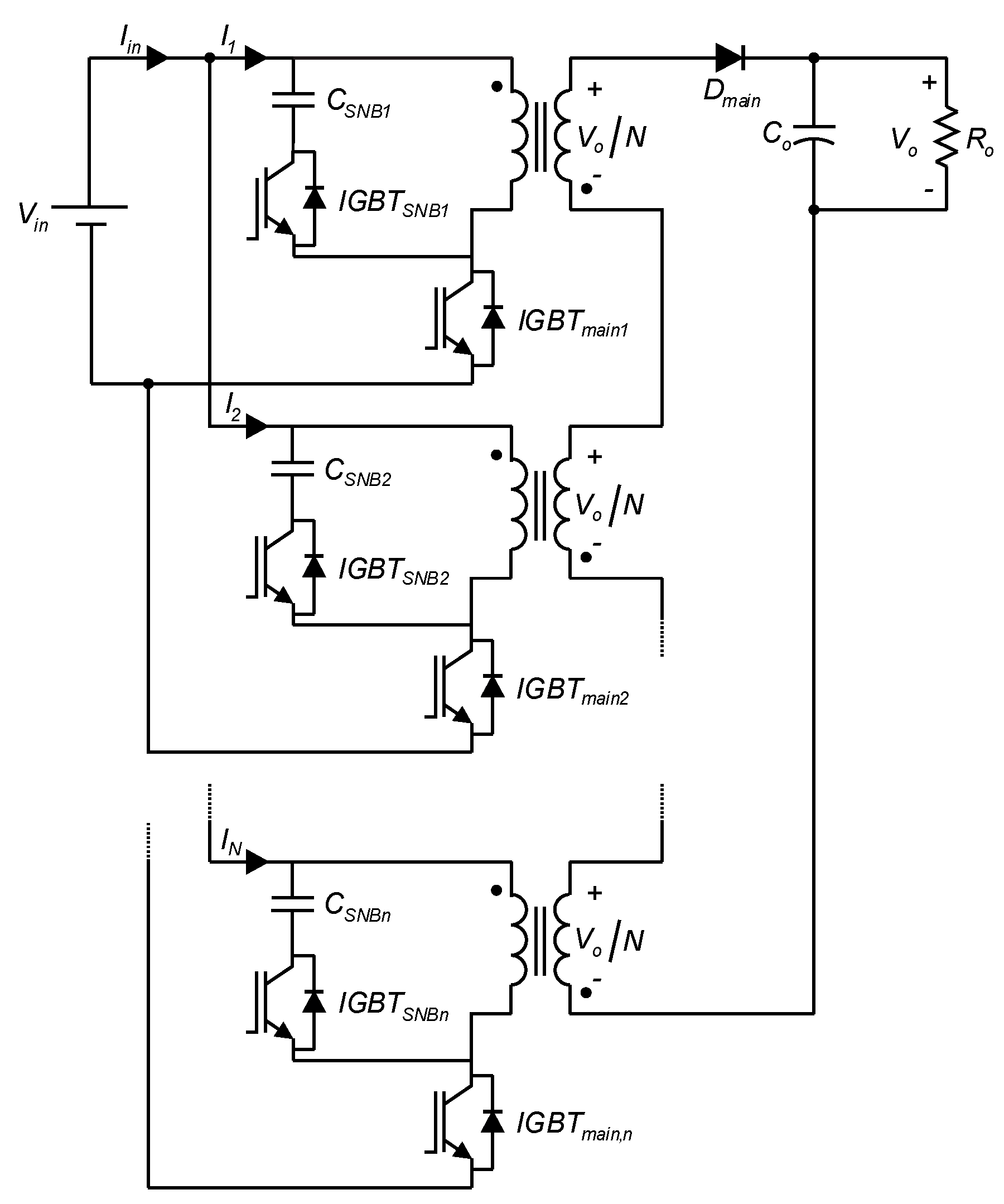
In this sense, the inclusion of active snubber networks is highlighted as an important contribution of this article. The topology proposed is depicted in Figure 2.
The different operation modes of the converter are presented and discussed. To validate the feasibility of the proposed converter, a laboratory prototype of 4.7 kW has been built and experimental results are presented considering a closed-loop voltage control scheme. Moreover, an efficiency analysis for the topology presented is carried out.
The paper is organized as follows. Section 2 describes the operating principle of the converter including voltage and current equations. Section 3 shows a mathematic derivation of the converter voltage transfer ratio. Section 4 describes the control scheme used for the proposed topology, Section 5 shows the experimental results obtained, and Section 6 presents a brief efficiency analysis of the converter. The conclusions of the work are stated in Section 7.

2. Operating Principle

The different operation modes of the proposed converter are analyzed under the following assumptions:
(1)
The output voltage has negligible ripple.
(2)
The coupled inductors (so called “flyback transformers”) are identical and have unity turns ratio.
(3)
The parameters of the flyback transformers are referred to the primary side.
(4)
The windings resistances are neglected.
(5)
The active snubber circuit returns the energy stored in the leakage inductance back to the supply.
(6)
The power semiconductor devices are ideal.
(7)
The converter operates in Discontinuous Conduction Mode (DCM).
(8)
Main switches and snubber switches cannot be closed at the same time. D 1 is the duty cycle for the main switch, and D 2 is the duty cycle for the snubber switch.

2.1. Operating Mode 1 ( 0 t t o n )

In this mode, all the main switches are closed, then the same current circulates in every inductor primary coil and main transistor (Figure 3a). The input voltage is applied to the input magnetizing inductance of every transformer and their leakage inductances store the energy supplied by the source. The diode D m a i n is reverse-biased and the capacitor C o discharges in the load resistor R o the energy stored in the last period. It can be shown that the peak current in every main switch S i with i = 1 N is given by:
I N m a x = V i n   D 1 ( L m + L l )     f s
where V i n is the converter supply voltage, D 1 is the duty cycle of the main switches, L m is the magnetizing inductance of each transformer, L l is the leakage inductance, and f s is the switching frequency of the converter. The voltage in the primary and secondary inductors are given by (2) and (3), respectively:
V p , N = V i n
V s , N = ( V i n a )
The voltage in the main diode is:
V D m a i n = ( N V i n a + V o )
with V o being the converter output voltage, a is the transformers turns ratio, and N is the number of flyback transformers. The output current is:
I o = V o R o = I C o
where I C o is the output capacitor current. On the other hand, the switches of every snubber circuit are opened. However, each snubber capacitor is charged with a voltage V C s n b ( 0 ) from the previous cycle. This voltage is determined by:
V C s n b ( 0 ) = I N m a x   L l 1 tan [ D 2   T s 2 L l   C s n b ] + V o
where T s is the switching period, C s n b is the snubber capacitor, and I N m a x is the maximum current in the main switch.
To obtain (6) it is necessary to define the current when the snubber is activated, which is defined by:
i s n b ( t ) = ( V o V C s n b ( 0 ) ) L l L l C s n b sin ( ω t ) + I ( 0 ) cos ( ω t )
where I ( 0 ) is the initial current (from the previous cycle) and the frequency is ω = 1 / L l C s n b . Then, the voltage V C s n b ( 0 ) shown in (6) is given by evaluating (7) at t = ( D 2 T s ) / 2 considering that the current i s n b ( D 2 T s 2 ) = 0 and I ( 0 ) = I N m a x (see Figure 4).

2.2. Operating Mode 2 ( t o n t t 1 )

In this mode, all the main switches are turned off and the snubbers diodes (in parallel with the snubber IGBTs) are conducting current (Figure 3b) from t = t o n to t = t 1 . However, although it will not conduct any current until t = t 1 , the snubber IGBT is triggered at t = t o n . This is performed for simplicity, since it would be very difficult to know precisely the instant t = t 1 as it depends on the leakage inductance (which is difficult to measure accurately).
The current in the magnetizing inductance L m circulates through the primary winding and the leakage inductance ( L l ). The current in the main diode is given by:
I D m a i n = i L m ( t ) I L l
The magnetizing inductance current i L m decreases linearly until the stored energy falls to zero in an instant t o n . The expression for the magnetizing inductance current is:
i L m ( t ) = ( I L m m a x   V o V i n D 1 T s t + I L m m a x ) + I L l
The current in the leakage inductance i L l equals the current in the snubber capacitor and is given by:
i L l ( t ) = i C s n b ( t ) = V o V C s n b ( 0 ) L l L l C s n b sin ( 1 L l C s n b t ) + I L m m a x cos ( 1 L l C s n b t )
and the voltage in the leakage inductance ( v L l ) is defined by:
v L l ( t ) = L l d i C s n b ( t ) d t = V o / N V C s n b ( 0 ) cos ( 1 L l C s n b t ) I L m m a x L l L l C s n b sin ( 1 L l C s n b t )
In this state, the voltage in the magnetizing inductance is V L m = V o . Then, the snubber capacitor voltage is:
v C S n b = V L l + V L m
At t = t 1 , the current in the snubber capacitor decreases to zero.

2.3. Operating Mode 3 ( t 1 t t 2 )

In this operating mode (Figure 3c), all the snubbers IGBT switches are turned on. There is an energy balance between the snubber capacitor and the leakage inductance. Therefore, the energy delivered by the inductor to the snubber capacitor is returned to the leakage inductance. Hence, the current in the leakage inductance at t = t 2 is maximum of value I L m m a x but with the opposite direction to operating mode 2.
At the end of this period, the output capacitor recovers its initial charge of operating mode 1. The blocking voltage of the main switches is given by:
V C E o f f = V L l ( t ) + V L m V i n = V L l ( t ) V o V i n
and the current in the main diode is defined by:
i D m a i n ( t ) = i L m ( t ) i L l ( t )

2.4. Operating Mode 4 ( t 2 t t 3 )

This operating mode is shown in Figure 3d. In this case, all the main IGBT switches are turned off but their anti-parallel diodes are conducting current. Therefore, the energy stored in the leakage inductance is delivered back to the input voltage source. The leakage inductance current decreases to zero. The main diode current begins to decrease and the voltage in the leakage inductance ( V L l ) is defined by:
V L l = V i n + V o / N
The instant t = t 3 corresponds to the time where the leakage inductance current falls to zero, and can be calculated with:
t 3 t 2 = V L l · D 2 T s 2   ( V i n + V o / N )
where V L l is the average voltage in the leakage inductance.

2.5. Operating Mode 5 ( t 3 t t 4 )

In this operating mode (shown in Figure 3e), the energy stored in the leakage inductance is totally delivered to the input supply. The main diode current decreases to zero at t = t 4 . The period where the main diode is conducting can be calculated as:
Δ t 4 = V i n D 1 T s V o / N
From t = t o n to t = t 4 , the output capacitor C o receives the energy stored in the magnetizing inductance, then its charge increases as well as its voltage.

2.6. Operating Mode 6 ( t 4 t T s )

In this mode, all the switches are turned-off, as shown in Figure 3f. The energy stored in the output capacitor is delivered to the load resistor. The current in the output capacitor is given by:
i C o ( t ) = I o
where the output current I o is imposed by the load.
The main waveforms obtained from the different operating modes are summarized in Figure 4 and Figure 5. In Figure 4, the magnetizing current I L m of the transformers (top), the main switches current I I G B T m a i n (middle) and the snubber switches current I I G B T s n b (bottom) are shown. Figure 5 shows the voltage in the main switches V C E m a i n (top), the current I D m a i n in the main diode (middle), and the gating signals of main and snubber IGBT switches (bottom).

3. Voltage Transfer Ratio

The voltage gain of the power converter is derived assuming equal input and output power P i n = V i n I i n = V o I o = P o = V o 2 / R o (no losses in the converter). The average current of the snubber switches (in a period) is zero (see Figure 4), and the average current of the main IGBT switches is defined by:
I I G B T m a i n = I N m a x D 1 2 I N m a x 2 L l   2   T s ( V i n + ( V o / N ) )
On the other hand, since the expression for I N m a x is given in (1), the total input average current I i n = N I I G B T m a i n is:
I i n = N V i n D 1 2 T s 2 ( L m + L l ) ( 1   L l   V i n   ( L m + L l ) ( V i n + ( V o / N ) ) )
Considering the above equations, it is obtained:
V o 2 V i n 2 = N D 1 2 R o   ( ( L m + L l ) ( 1 + V o V i n N ) L l ) 2 f s   ( L m + L l ) 2   ( V o V i n N + 1 )
Defining X = V o / V i n , Equation (21) can be rewritten as:
X 3 + 1 N X 2 D 2 R o N 2 f s   ( L m + L l ) X D 2 N 2 R o 2 f s ( L m + L l ) ( L l L m + L l + 1 ) = 0
This third-order equation is solved using the Cardano method [22], and for the parameters considered in this work, it has two real negative roots and one positive real root. Since the converter does not invert the polarity of the input voltage, only the positive root is valid, therefore the voltage transfer ratio (VTR) of the topology proposed is:
V o V i n = D 1 N   R o 2   f s   ( L m + L l )

4. Control Scheme

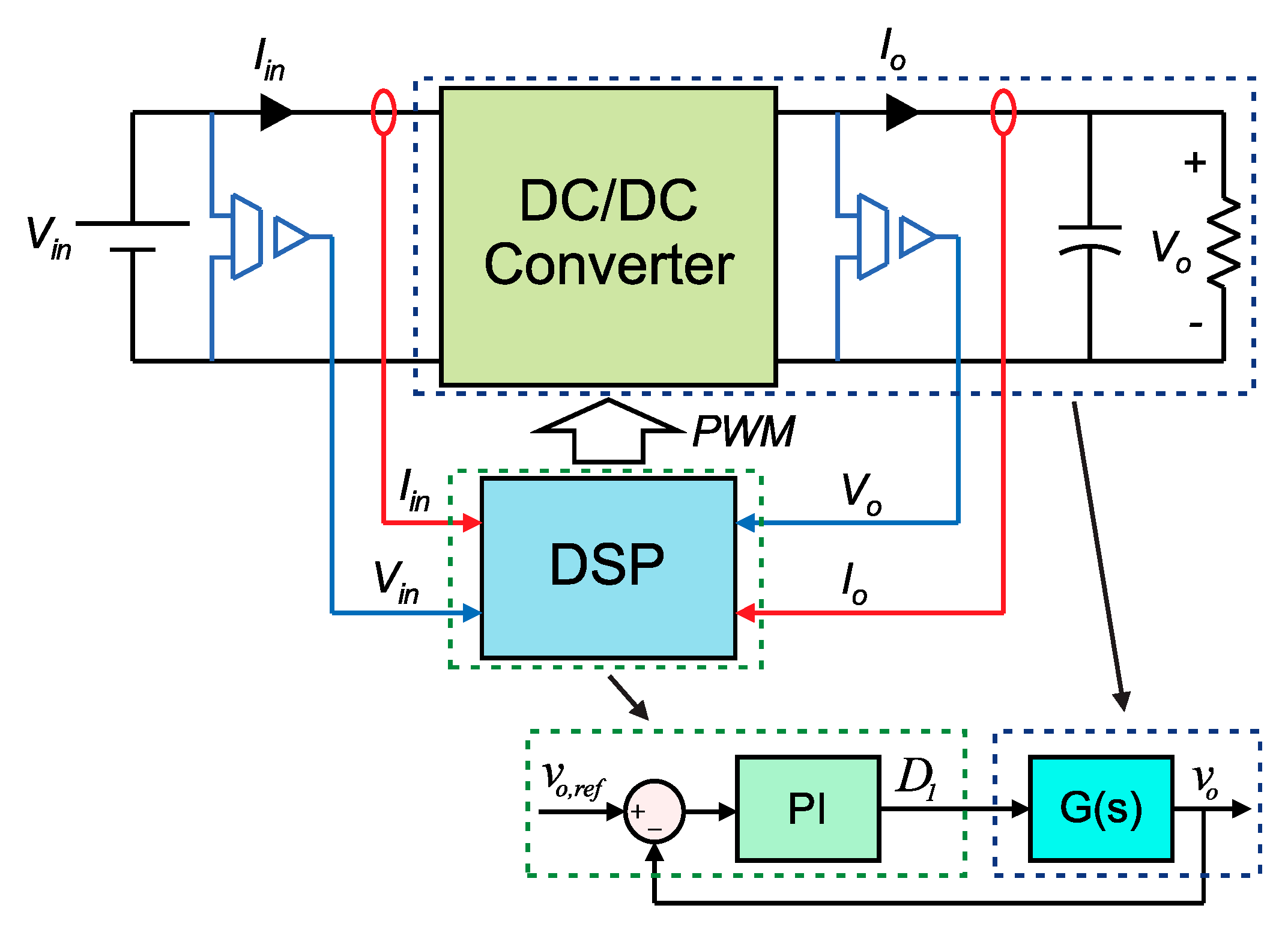
A voltage control scheme is proposed for the topology. A Proportional+Integral (PI) controller processes the difference between a reference voltage and the output measured voltage. The output of the PI controller is intended to be the duty cycle of the converter D 1 and is limited in the range 0–0.65. The upper limit, so-called critical duty cycle ( D 1 c r i t = 0.65 ), is set to avoid operation in Continuous Conduction Mode (CCM) as DCM operation offers advantages in term of control simplicity and converter efficiency [17]. For DCM operation, D 1 T s + Δ t 4 < T s must be fulfilled. To operate with a safety margin, it is stated that D 1 T s + Δ t 4 0.96 T s to ensure DCM. The main duty cycle D 1 is defined by (23) and is dependent on the load (which is constant in this case). On the other hand, Δ t 4 is defined by (17) then the critical duty cycle D 1 c r i t is given by:
D 1 c r i t 0.96   V i n D 1 ( V o / N )
For controller design purposes, the transfer function G ( s ) considered (output voltage/main switch duty cycle) is given by:
G ( s ) = V o ( s ) D 1 ( s ) = V i n   N R o 2 ( L m + L l ) f s   ( 1 + s R s e C o s R o C o + 1 )
where R s e is the series-equivalent resistance of the output capacitor. As can be noted in (25), the transfer function depends on the load resistor R o . As the output voltage and current are measured, the value of the load resistor can be easily calculated by R o = V o / I o . Then the controller parameters are calculated (in a real-time Digital Signal Processor) every sampling period to adapt to the load. For controller design purposes, the closed-loop transfer function of the system is obtained:
M ( s ) = A ω c ( K p s + K i ) R o C o s 3 + s 2 ( 1 + R o C o ω c ) R o C o + s ( ω c + A ω c K p ) R o C o + A ω c K i R o C o
where A = V i n R o N 2 f s ( L m + L l ) · ( 1 + R s e C o ) ( R s e is the equivalent series resistor of the output capacitor).
The parameters K p and K i of the controller are then calculated by equating the denominator of (26) to the characteristic third-order polynomial ( p ( s ) = ( s + α o ) ( s 2 + 2 ξ ω n s + ω n 2 ) ). Therefore, the proportional and integral constants of the controller are:
K p = ( 2 ξ ω n   ( 1 + R o C o ω c ) R o   C o ( 2 ξ ω n ) 2 + ω n 2 ) R o C o ω c V i n   ω c   R o N 2   f s   ( L m + L l ) ( 1 + R s e C o )
K i = ω n 2   R o C o ( ( 1 + R o C o ω c ) R o C o 2 ξ ω n ) V i n ω c R o N 2 f s ( L m + L l ) · ( 1 + R s e C o )
where ω n is the natural frequency of the control loop, ξ is the damping ratio, and ω c is the cut-off frequency of a low-pass filter used in the measurement of V o . The values considered in this work are ω n = 2100   [ rad / s ] , ξ = 0.8 and ω c = 2000 π   [ rad / s ] . In Figure 6, a diagram of the control scheme is shown.
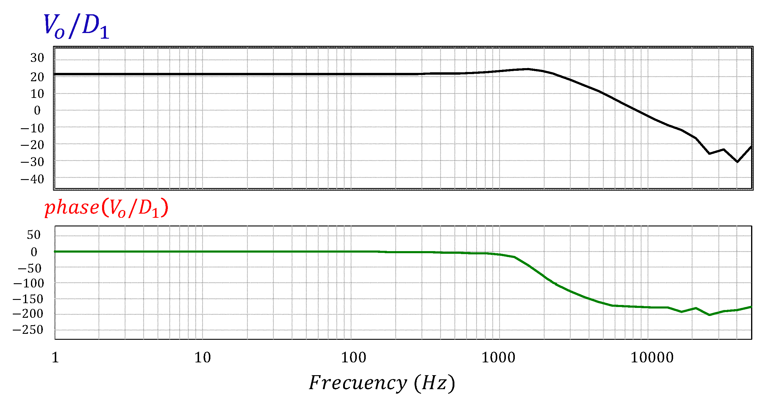
The Bode diagrams of the system in the open-loop and closed-loop are shown in Figure 7 and Figure 8, respectively:
From Figure 7, it can be noted that the phase margin in the open-loop operation of the converter is zero as well as the gain margin; then the system is instable and requires a feedback controller. When the voltage controller is included, the Bode diagram (Figure 8) shows a phase margin of about 70° and an infinity gain margin (as the phase (Figure 8 bottom) never crosses the −180° line), then confirming the stability of the closed-loop system.

5. Experimental Results

To validate the proposed topology, a laboratory prototype with four flyback modules has been built. In this work, the maximum output power extracted from the converter is 4.7 kW; however, the prototype has been constructed considering a larger power for future research. Each transformer is rated at 5 kW, aiming to obtain 20 kW with four flyback stages. The semiconductors were also selected considering an output power of 20 kW. The full power converter is aimed to be used in electrical drives applications such as: electric traction using DC machines and DC supply for three-phase inverters driving AC machines among others. The experimental system is shown in Figure 9.
The input supply consists of eight series-connected 12V AGM batteries. The main switches are IGBTs model STGW35HF60WD and the model of the main diode is STTH9012TV; the snubber switch is an IGBT model NGTB50N120FL2WG.
The flyback converter transformers (Figure 10) are built with a two-column ferrite core having a 3 [mm] airgap. The transformers parameters (referred to the primary side) are R p = 4 [ m Ω ] (primary coil resistance), L l = 10 [ μ H ] (leakage inductance), L m = 170 [ μ H ] (magnetizing inductance) and R c 300 [ k Ω ] (resistance of core losses); the turns ratio is 24 : 24 a = 1 .
The output capacitor is a polypropylene-type for low equivalent series-resistance ( R s e = 2   m Ω ). The control system was implemented with a Texas DSP28335 microprocessor, and the gating signals are transmitted to the converter via optical fiber. The experimental parameters are shown in Table 1.
The converter has been tested at rated power in steady state operation. The time period for the experimental waveforms of Figure 11, Figure 12, Figure 13 and Figure 14 is 200 µs. Figure 11 shows the currents of the main IGBT switches. The negative peaks are due to the regeneration process where energy is returned to the DC supply.
Figure 12 shows the collector-emitter voltage of the main switches while Figure 13 shows the current of a main switch (blue) along with the current of the corresponding snubber switch (purple). Figure 14 shows the main diode current. The similarity between the experimental waveforms (Figure 11, Figure 12, Figure 13 and Figure 14) and the theoretical waveforms (Figure 4 and Figure 5) is evident.
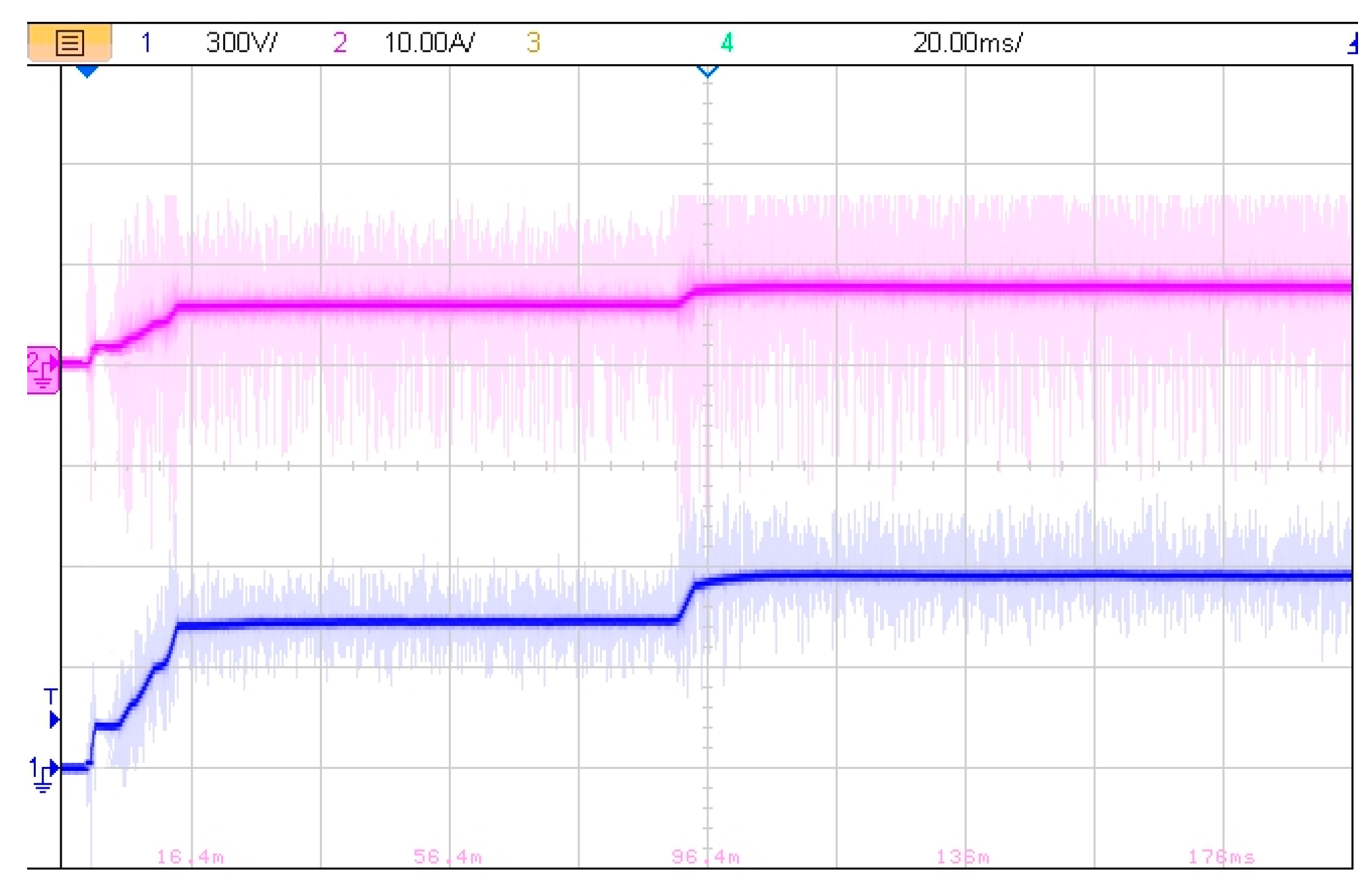
To study the performance of the voltage control scheme, reference voltage changes and load impacts have been tested. Figure 15 shows the output voltage (purple) where a gradual increment in the reference voltage from 0 to 500 V is applied at the beginning. Then, when steady state is achieved, a step change in the reference voltage from 500 V to 590 V is carried out. Figure 15 (blue) shows the output current which presents the same waveform as the output voltage due to the resistive characteristic of the load. This current finally stabilizes to ~8 A for an output power of 4720 W.
Finally, Figure 16 shows the output voltage (blue) and current (purple) during a load impact. The voltage reference is set to 590 V and a load impact that increases the current from 1 A to 6 A is applied. The output voltage is stabilized in about 3 ms. Both Figure 15 and Figure 16 verify the effectiveness of the voltage control strategy implemented.
A summary of values obtained from experimental and simulation results is shown in Table 2.

6. Efficiency Analysis

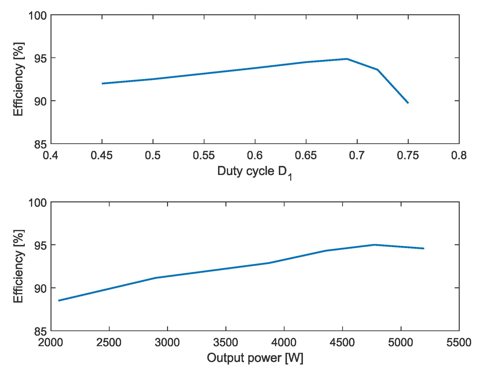
An efficiency study, based on experimental tests of the converter built, has been carried out. A first analysis was performed in open-loop operation of the converter, with constant load and different duty cycles. The results obtained are shown in Table 2, where P o and P i n are the output and input power, respectively. The efficiency is calculated as η = 100 ( P o u t P i n ) . It is observed that the highest efficiencies are achieved by operating the converter with duty cycles in the range 0.6–0.7. For duty cycles over 0.7, the efficiency decreases due to higher conduction losses in the switches and passive elements. It is worth mentioning that, as stated in Section 4, for duty cycles over 0.65, the converter operates in CCM mode. This is done only for efficiency evaluation purposes.
A second analysis was carried out with closed-loop control operation. The output voltage V o is kept constant and maximum (590 V), and the output current is variable (variable load). The results are presented in Table 3. A maximum efficiency of 95% is obtained for an output power of 4.77 kW. Figure 17 summarizes the results shown in Table 3 and Table 4.

7. Conclusions

In this paper, a DC-DC converter topology based on a standard flyback converter has been proposed. The converter proposed is modular and considers a reduced number of power devices compared to flyback interleaved topologies.
Active snubber circuits are included to avoid excessive voltages in the main power switches. The different operating modes of the converter are described and mathematically analyzed.
A simple voltage control scheme is proposed considering discontinuous conduction mode operation, obtaining a good performance under load impacts and voltage variations.
A laboratory prototype has been built and experimental results were obtained, showing a good performance of the converter and its control scheme in steady state operation as well as during transient operation.
The proposed converter results are competitive in terms of cost and efficiency with respect to the flyback interleaved topologies. The obtained full load efficiency of the proposed converter is 95% resulting in an attractive alternative for nowadays industrial requirements.

Author Contributions

Conceptualization, C.P. and R.P.; Methodology, C.M. and W.J.; software, C.P.; validation, C.P., C.M. and R.V.; formal analysis, R.P. and J.R.; investigation, C.P.; resources, C.P., R.P. and R.V.; data curation, C.M. and W.J.; writing—original draft preparation, J.R. and C.P.; writing—review and editing, J.R.

Funding

This research was funded by UNIVERSIDAD DE LA FRONTERA, project DIUFRO number DI19-0013 and by the Chilean Council of Scientific and Technological Research under projects CONICYT/FONDEF/ID17I10421, CONICYT/FONDECYT/11180092 and CONICYT/FONDAP/15110019.

Acknowledgments

In this section you can acknowledge any support given which is not covered by the author contribution or funding sections. This may include administrative and technical support, or donations in kind (e.g., materials used for experiments).

Conflicts of Interest

The authors declare no conflict of interest.

References

  1. Singh, S.; Singh, B. Improved power quality flyback converter fed PMBLDCM drive. In Proceedings of the 5th IEEE India International Conference on Power Electronics (IICPE), Delhi, India, 6–8 December 2012; pp. 1–5. [Google Scholar]
  2. Babadi, A.; Pour, A.; Amjadifard, R. Improved source-end current Power Quality performance of a BLDC motor drive using a novel DC-DC converter. In Proceedings of the Iranian Conference on Electrical Engineering (ICEE), Tehran, Iran, 2–4 May 2017; pp. 1360–1365. [Google Scholar]
  3. Rizzoli, G.; Zarri, L.; Wang, J.; Shen, Z.; Burgos, R.; Boroyevich, D. Design of a two-switch flyback power supply using 1.7 kV SiC devices for ultra-wide input-voltage range applications. In Proceedings of the IEEE Energy Conversion Congress and Exposition (ECCE), Milwaukee, WI, USA, 18–22 September 2016; pp. 1–5. [Google Scholar]
  4. Perrin, R.; Quentin, N.; Allard, B.; Martin, C.; Ali, M. High-Temperature GaN Active-Clamp Flyback Converter with Resonant Operation Mode. IEEE J. Emerg. Sel. Top. Power Electron. 2016, 4, 1077–1085. [Google Scholar] [CrossRef]
  5. Mazumdar, P.; Enjeti, P.; Balog, R. Analysis and Design of Smart PV Modules. IEEE J. Emerg. Sel. Top. Power Electron. 2014, 2, 451–459. [Google Scholar] [CrossRef]
  6. Lodh, T.; Pragallapati, N.; Agarwal, V. Novel Control Scheme for an Interleaved Flyback Converter Based Solar PV Microinverter to Achieve High Efficiency. IEEE Trans. Ind. Appl. 2018, 54, 3473–3482. [Google Scholar] [CrossRef]
  7. Kashif, M. Bidirectional flyback DC-DC converter for hybrid electric vehicle: Utility, working and PSPICE computer model. In Proceedings of the Asia Pacific Conference on Postgraduate Research in Microelectronics and Electronics, Hyderabad, India, 5–7 December 2012; pp. 61–66. [Google Scholar]
  8. Bhattacharya, T.; Giri, V.; Mathew, K.; Umanand, L. Multiphase Bidirectional Flyback Converter Topology for Hybrid Electric Vehicles. IEEE Trans. Ind. Electron. 2009, 56, 78–84. [Google Scholar] [CrossRef]
  9. Shen, C.; Chiu, P. Buck-boost-flyback integrated converter with single switch to achieve high voltage gain for PV or fuel-cell applications. IET Power Electron. 2016, 9, 1228–1237. [Google Scholar] [CrossRef]
  10. Yigeng, H.; Yu, W. A robust flyback converter based on high order sliding mode control for fuel cell. In Proceedings of the 40th Annual Conference of the IEEE Industrial Electronics Society (IECON), Dallas, TX, USA, 29 October–1 November 2014; pp. 3936–3940. [Google Scholar]
  11. Cheng, H.; Chang, Y.; Chang, C.; Hsieh, S.; Cheng, C. A Novel High-Power-Factor AC/DC LED Driver with Dual Flyback Converters. IEEE J. Emerg. Sel. Top. Power Electron. 2019, 7, 555–564. [Google Scholar] [CrossRef]
  12. Tseng, S.-Y.; Huang, P.-J.; Wu, D.-H. Power Factor Corrector with Bridgeless Flyback Converter for DC Loads Applications. Energies 2018, 11, 3096. [Google Scholar] [CrossRef]
  13. Kazimierczuk, M. Pulse-width Modulated DC–DC Power Converters, 1st ed.; John Wiley & Sons: Hoboken, NJ, USA, 2008. [Google Scholar]
  14. Lin, B.; Hsieh, F. Soft-Switching Zeta–Flyback Converter with a Buck–Boost Type of Active Clamp. IEEE Trans. Ind. Electron. 2007, 54, 2813–2822. [Google Scholar]
  15. Pagliosa, M.; Faust, R.; Lazzarin, T.; Barbi, I. Input-series and output-series connected modular single-switch flyback converter operating in the discontinuous conduction mode. IET Power Electron. 2016, 9, 1962–1970. [Google Scholar] [CrossRef]
  16. Rezaei, M.; Lee, K.; Huang, A. A High-Efficiency Flyback Micro-inverter With a New Adaptive Snubber for Photovoltaic Applications. IEEE Trans. Power Electron. 2016, 31, 318–327. [Google Scholar] [CrossRef]
  17. Tamyurek, B.; Kirimer, B. An interleaved high-power flyback inverter for photovoltaic applications. IEEE Trans. Power Electron. 2015, 30, 3228–3241. [Google Scholar] [CrossRef]
  18. Zumel, P.; García, O.; Oliver, J.; Cobos, J. Differential-Mode EMI Reduction in a Multiphase DCM Flyback Converter. IEEE Trans. Power Electron. 2009, 24, 2013–2020. [Google Scholar] [CrossRef] [Green Version]
  19. Dong, M.; Tian, X.; Li, L.; Song, D.; Wang, L.; Zhao, M. Model-Based Current Sharing Approach for DCM Interleaved Flyback Micro-Inverter. Energies 2018, 11, 1685. [Google Scholar] [CrossRef]
  20. Pesce, C.; Blasco Gimenez, R.; Riedemann, J.; Andrade, I.; Pena, R. A DC-DC Converter Based on Modified Flyback Converter Topology. IEEE Lat. Am. Trans. 2016, 14, 3949–3956. [Google Scholar] [CrossRef]
  21. Alganidi, A. A Comparison between Different Snubbers for Flyback Converters. Master’s Thesis, The University of Western Ontario, London, ON, Canada, 2017. Available online: https://ir.lib.uwo.ca/etd/5153 (accessed on 22 May 2019).
  22. Kreyszig, E. Advanced Engineering Mathematics, 10th ed.; John Wiley & Sons: Hoboken, NJ, USA, 2010. [Google Scholar]
Figure 1. Architectures of modular flyback converters: (a) IPOP, (b) IPOS, (c) ISOS, (d) ISOP.
Energies 12 02066 g001
Figure 2. Proposed topology.
Energies 12 02066 g002
Figure 3. Equivalent circuits for each operating mode: (a) Mode 1; (b) Mode 2; (c) Mode 3; (d) Mode 4; (e) Mode 5; (f) Mode 6.
Energies 12 02066 g003aEnergies 12 02066 g003b
Figure 4. Theoretical waveforms of I L m (top), I I G B T m a i n (middle) and I I G B T s n u b b e r .
Energies 12 02066 g004
Figure 5. Theoretical waveforms of V C E m a i n (top), I D m a i n (middle) and gating pulses of main and snubber IGBT switches (bottom).
Energies 12 02066 g005
Figure 6. Control scheme.
Energies 12 02066 g006
Figure 7. Open-loop Bode diagram of the system.
Energies 12 02066 g007
Figure 8. Closed-loop Bode diagram of the system.
Energies 12 02066 g008
Figure 9. Experimental laboratory prototype.
Energies 12 02066 g009
Figure 10. Ferrite core flyback transformers.
Energies 12 02066 g010
Figure 11. Main IGBT switches currents (Scale: 40 A/div).
Energies 12 02066 g011
Figure 12. Main IGBT switches collector-emitter voltages (Scale: 500 V/div).
Energies 12 02066 g012
Figure 13. Main switch current (blue–Scale: 40 A/div) and snubber current (purple–Scale: 40 A/div).
Energies 12 02066 g013
Figure 14. Main diode current (Scale: 25 A/div).
Energies 12 02066 g014
Figure 15. Output voltage V o (purple-Scale: 300 V/div) and output current I o (blue-Scale: 10 A/div). Total time: 200 ms.
Energies 12 02066 g015
Figure 16. Output voltage V o (blue-Scale: 150 V/div) and output current I o (purple-Scale: 5 A/div). Total time: 10 ms.
Energies 12 02066 g016
Figure 17. Efficiency of the converter for constant load/variable duty cycle (top) and constant duty cycle/variable load (bottom).
Energies 12 02066 g017
Table 1. Experimental parameters.
VariableDescriptionValueVariableDescriptionValue
V i n Input voltage 96   V C o Output capacitor 320   μ F
V o Rated output voltage 590   V f s Switching frequency 10   kHz
L m Magnetizing inductance 170   μ H N Number of stages 4
n P / n S Transformers turns ratio1 P o Rated power 4700 W
Table 2. Summary of experimental and simulation values obtained.
Power Device Experimental ResultsSimulation Results
Main Switch
 - Positive peak current:32 A31.5 A
 - Negative peak current:16 A15.3 A
 - Maximum collector-emitter voltage:400 V398.5 A
Snubber Switch
 - Positive peak current:24 A23.3 A
 - Negative peak current:32 A31.3 A
Main Diode
 - Maximum current:57 A56.2 A
Table 3. Efficiency results with constant load.
D 1 V o   [ V ] I i n   [ A ] P o   [ W ] P i n   [ W ] η   [ % ]
0.4538223.672091227391.99
0.542529.072581279092.50
0.651041.283717396393.79
0.6555348.104362461694.49
0.6958953.964916518294.86
0.7261258.945353571993.60
0.7563764.575808647489.71
Table 4. Efficiency results with constant output voltage.
I o   [ A ] I i n   [ A ] P o   [ W ] P i n   [ W ] η   [ % ]
3.524.32065233388.51
4.9133.12897317891.15
6.5643.413870416792.88
7.3848.094354461694.32
8.0952.344773502495.00
8.8157.255198549694.57