Article

Multi-Domain Modelling of LEDs for Supporting Virtual Prototyping of Luminaires

1
Department of Electron Devices, Budapest University of Technology and Economics, Magyar tudósok körútja 2, bldg. Q, 1117 Budapest, Hungary
2
Mechanical Analysis Division, Mentor, a Siemens Business, Gábor Dénes utca 2, 1117 Budapest, Hungary
*
Author to whom correspondence should be addressed.
Energies 2019, 12(10), 1909; https://doi.org/10.3390/en12101909
Submission received: 5 April 2019 / Revised: 11 May 2019 / Accepted: 14 May 2019 / Published: 18 May 2019
(This article belongs to the Special Issue Thermal and Electro-thermal System Simulation)

Abstract

:
This paper presents our approaches to chip level multi-domain LED (light emitting diode) modelling, targeting luminaire design in the Industry 4.0 era, to support virtual prototyping of LED luminaires through luminaire level multi-domain simulations. The primary goal of such virtual prototypes is to predict the light output characteristics of LED luminaires under different operating conditions. The key component in such digital twins of a luminaire is an appropriate multi-domain model for packaged LED devices that captures the electrical, thermal, and light output characteristics and their mutual dependence simultaneously and consistently. We developed two such models with this goal in mind that are presented in detail in this paper. The first model is a semi analytical, quasi black-box model that can be implemented on the basis of the built-in diode models of spice-like circuit simulators and a few added controlled sources. Our second presented model is derived from the physics of the operation of today’s power LEDs realized with multiple quantum well heterojunction structures. Both models have been implemented in the form of visual basic macros as well as circuit models suitable for usual spice circuit simulators. The primary test bench for the two circuit models was an LTspice simulation environment. Then, to support the design of different demonstrator luminaires of the Delphi4LED project, a spreadsheet application was developed, which ensured seamless integration of the two models with additional models representing the LED chips’ thermal environment in a luminaire. The usability of our proposed models is demonstrated by real design case studies during which simulated light output characteristics (such as hot lumens) were confirmed by luminaire level physical tests.

1. Introduction

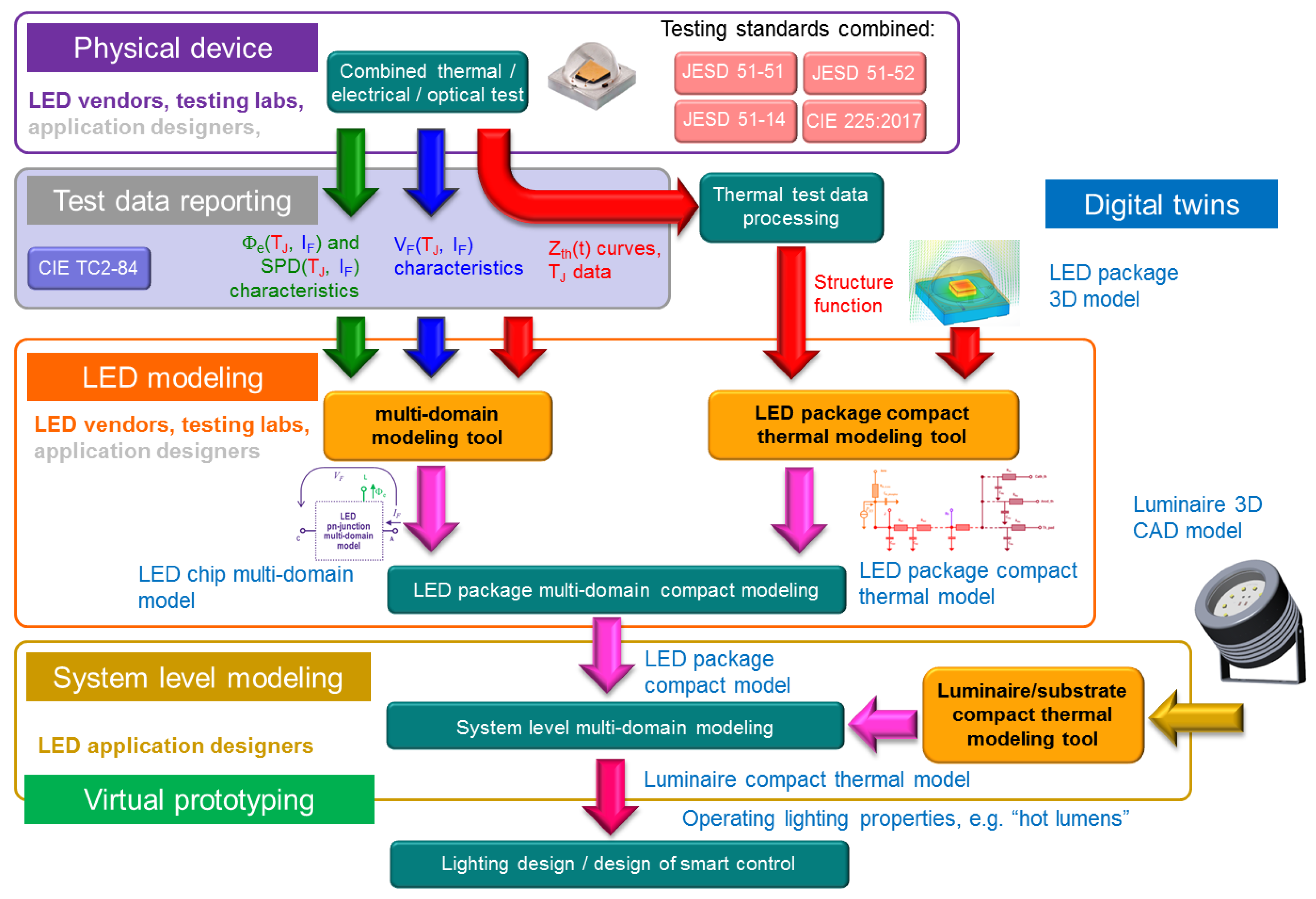
1.1. The Context of this Work

In previous decades, the design of light sources (incandescent, fluorescent) and luminaires were separated. The light sources were not sensitive to the ambient temperature, luminaire design was restricted mainly to the optics, and the electric and thermal coupling of the two worlds occurred at the socket, in both physical and conceptual sense.
With the advent of LED light sources, thermal aspects in luminaire design have become important because LEDs are very sensitive to heat. The “sockets” ceased to exist, and the close thermal coupling of luminaires and LEDs thus requires sophisticated electronic cooling design tools, such as CFD (computational fluid dynamics) based simulators.
Nowadays, the LED luminaire design is characterized by the presence of re-organized successors of previously known major players of the traditional lighting industry and also of many new, smaller start-up companies. These major companies have lots of expertise in the use of advanced CFD software for thermal-only simulations while start-ups have much less expertise and resources. The goal of the Delphi4LED project [1,2] is to develop new LED luminaire design workflows for both types of companies to support them in significantly reducing design costs and time-to-market [3,4], through virtual prototyping of luminaires, i.e., computer simulation of the luminaire. Figure 1 illustrates the process of creating simulation models at different integration levels, from the physical testing of LEDs, and creation of their simulation models to the use of LEDs at the higher level integration of a solid-state lighting product (e.g., a luminaire).
Inputs to such a digital design flow of LED luminaires are the overall lighting requirements, such as targeted minimal light output under application conditions, allowed maximal input electrical power, driver and optics efficiency, etc., to support the design of optimized LED luminaires through multi-domain simulations [3,4].
In the bottom-up modular approach, the modelling starts from a multi-domain model of LED chips [5,6,7], followed by compact thermal models of the LED packages, modules (orange framed items in Figure 1), and finally, luminaires [8,9]. Details of the compact modelling of the 3D thermal environment of LED chips (package, substrate, luminaire with optics) are provided in other publications, such as [8,10,11]. In the “Industry 4.0” language, these simulation models are called “digital twins” to represent the relevant aspects of the physical samples of LED chips, LED packages, modules, etc. [3,4]. Thus, the ultimate goal is to be able to predict the total emitted luminous flux [12] of different versions of a luminaire under thermally different application conditions (also referred to by the sloppy English term “hot lumens”).

1.2. The Wider Background

Many research teams have realized the importance of characterizing LEDs in multiple domains of operation. Mostly, these studies used empirical and sometimes rough approximations to obtain model parameters from measured data, see, e.g., [13,14,15,16,17]. In [13], an emphasis was placed on modelling LEDs’ efficiency. The authors of [14] with their ambitious target design of retrofitted LED lamps, used the photo-electro-thermal theory, which in our view is a relatively rough, empirical way of describing LED behavior. The authors of [15,16,17] in their work relied on LED characterization tools that have been introduced to the SSL industry as a result of our team’s pioneering work in multi-domain characterization [18,19]. In [15,16,17] (that are representative examples of the literature in the field), certain aspects of the junction temperature affected LED operating parameters were investigated, such as the electrical power [15], efficiency [16], and luminous flux [17]. However, none of these academic teams modelled LEDs using a holistic approach for daily use in industrial LED luminaire design flows, therefore, their studies were typically restricted to a few samples of certain LED types only.
Naturally, LED vendors have to support their customers. Therefore they usually publish different simulation models and other parts’ data, which is needed for the electrical, mechanical, optical, and manufacturing design of LED modules/luminaires. Thus, their electronically published data include Spice diode model parameters for their LEDs as well, see, e.g., [20,21]. Some common properties of these parameter sets are that they target the modeling of only the electrical behavior of LEDs, though certain parameter sets also allow simulation of the I-V (current-voltage) characteristics at any assumed junction temperature in the range of the validity of the model. Other vendors provide model data allowing simulation only at a 25 °C junction temperature, strongly limiting the applicability of such a diode model applied to an LED. The problem of the usual Spice models of LED vendors is that the standard Spice diode model is not an electro-thermal one: It does not support a fully-coupled electro-thermal simulation. Spice network solvers—with a few exceptions like [22]—are not fully-coupled electro-thermal solvers either. Finally, in standard Spice, there are no built-in means for predicting the light output properties of LEDs consistently with the electrical characteristics and the junction temperature. Due to these limitations of the commercially available tools and model parameter sets provided by LED vendors, a few academic research teams (including ours as well) have devoted their efforts to LED multi-domain modeling.
Thus, there have been a few other academic teams who published their results roughly at the same time as we also published our first multi-domain LED model, which aimed for general application. The first author whom we have to mention is A. Keppens, who, in his PhD dissertation about LED modeling [23], provides a comprehensive overview about the current and temperature dependence of the major parameters for about 12 different power LEDs. His experimental results include the electrical characteristics of power LEDs from the microampere range up to the forward current ranges of practical operation (100 mA and above). Besides the I-V characteristic section corresponding to the classical Shockley model of pn-junctions, parasitic effects at very small currents (different leakage currents) and high currents (e.g., the influence of the diode internal series resistance) are also treated. This early work, however, did not attempt to model the multi-domain operation of LEDs, i.e., to describe the mutual dependence of the electrical and thermal operation and light emission.
The first macro-type LED models with a real multi-domain approach aimed for Spice solvers were published by C. Negrea et al. [24] and K. Górecki [25], independently. Following our early approach [19], they both intended to simulate LEDs’ electrical, thermal, and optical properties simultaneously and consistently. Negrea’s team relied on the built-in diode model of Spice. As discussed above, this model is not an electro-thermal capable one, so in [24], a relaxation type iteration is used to reach consistent electro-thermal simulation results. This iteration scheme also includes light output modelling. In contrast to Negrea’s approach, in Górecki’s works (such as [25,26,27]), a self-built Spice circuit macro is used to represent an LED, assuring consistency among the three operating domains consistently, without any need for an additional iteration loop external to the Spice solver. Over the last couple of years, a continuous evolution of Górecky’s LED Spice model has been observed, resulting in an even newer model [28], which is still aimed at the calculation of the illuminance provided by the investigated LED. Illuminance, though, is not the property of the LEDs investigated, but it is a property that characterizes a given lighting situation, depending on the emitted total luminous flux of the light source and the geometrical arrangement of the lighting task. In their most recent model version [29] however, Gorecki and Ptak already calculate the primary light output properties: the radiant flux and the luminous flux.
These academic works did not have the ambition of developing a comprehensive multi-domain characterization and modelling methodology of power LEDs aimed at industrial application design flows, like those briefly discussed already and described in detail in [3,4]. Therefore, these studies were restricted to a few selected LED types, used as case studies only. In the work we present here, on the contrary, the models were applied to 5 to 20 samples of many different LED types, which are representative of today’s industrial LED luminaire designs.
The results of our academic approach that was the starting point of our most recent developments are summarized in [5]. The steps of the evolution of our models from this academic study towards our present, industrial application oriented models were published in our recent conference papers [6,7]. In the subsequent sections of this paper, we report the latest achievements in chip level modelling of LEDs with a focus on the thermally influenced electrical and optical behavior treated in a self-consistent manner, with the needs of commercial implementation for industrial applications in mind, in a closer context as presented in Section 1.1.

1.3. Overall Considerations Regarding Multi-Domain Chip Level Modelling of LEDs Aimed at Use in Industrial Application Design Flows

Luminaires are characterized mainly in their stationary “hot” state, therefore, it is satisfactory to construct LED models for a constant current bias, I F , and stabilized junction temperature, T J . However, it must be noted that I F is forced by the driving electronics, but T J is determined by the ambient temperature, T a m b , and the actual thermal boundary, both in a simulation environment and in real life.
We have shown previously that thermal transient measurements can deduce the R t h j a junction to ambient thermal resistance of the device along with the measurement system around it [30]. During physical tests of LEDs, R t h j a is used in an iterative process to control T a m b such that a target T J is reached. Thus, electric and radiometric properties can be measured at a programmed I F ,   T J operating point [31,32]. To obtain the thermal metrics, such as the junction-to-case thermal resistance ( R t h J C ), the applicable standard [33] prescribes thermal transient measurements at varying boundaries.
The Delphi4LED project targeted the elaboration of an automated process, which provides all modelling parameters in electrical, thermal, and optical domains, obtained in a single mechanical mounting of an LED or a compound of more LEDs in a combined thermal transient and radiometric measurement system [34].
In a round-robin test [35] (preceding measurement and modelling of dozens of LED types and hundreds of LED samples), the minimal number of I F and T J pairs was identified, which covered the foreseen design space of luminaires: The current range spanned from a few milliamps to amperes, and junction temperatures ranged from 15 °C to about 120 °C. Measurements also included the current region where the LEDs’ efficiency peaks (see Figure 2). In all cases, we could observe the characteristic decay of the light output at high currents termed the “light droop”.

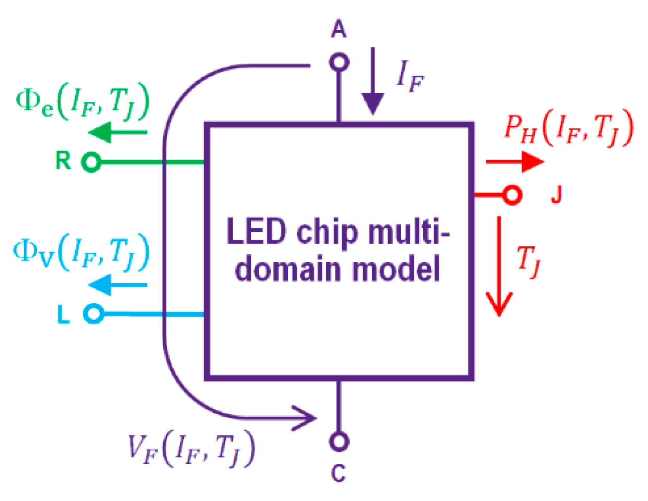
1.4. Expectations for a Chip Level Multi-Domain LED Model

An LED model aimed at the above outlined luminaire level simulations must be a functional one, and provide a set of simple analytic formulae. The same set should portray all power LEDs, each having a different complex material and geometry composition. A small number of numeric parameters must be assigned to the formulae to depict one distinctive LED type in all the three mutually dependent operating domains.
The proposed models provide the forward voltage, V F , between the A (anode) and C (cathode) electrical terminals and the fluxes, leaving the LED as a function of a forced forward current, I F , and junction temperature, T J (Figure 3). The fluxes we are interested in are:
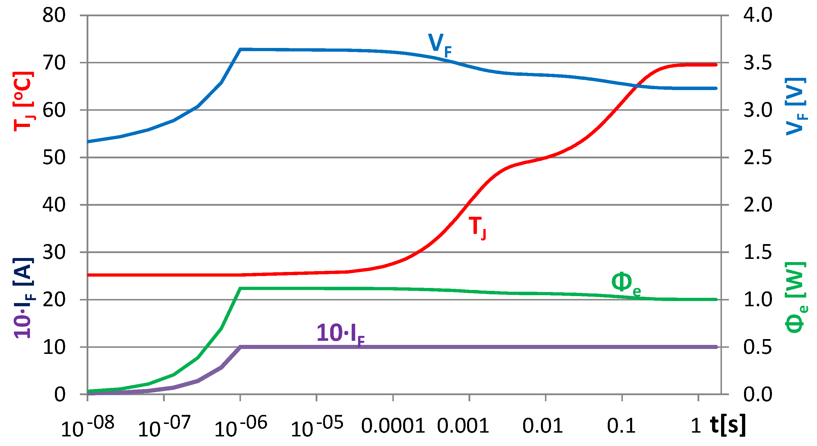
  • The heat-flux (also known as the real heating power, P H leaving the device through the thermal junction node denoted by J.
  • The total emitted radiant flux, Φ e [36] (also known as the optical power, P o p t ), leaving the device through the optical port of the model denoted by R.
  • The total emitted luminous flux, Φ V [12], leaving the device through the optical port of the model denoted by L.
During the Delphi4LED project, we developed two different modeling approaches. Already, at the very beginning, a generic analytical model, which can be generated directly from the measured electrical and optical data with precise parameter fitting, primarily based on Shockley’s model of semiconductor diodes, was required. The ultimate model version that we present in this paper can be used by “electrical only” circuit simulators, like the popular Spice program, freely available at many sites, such as LTspice, thus yielding accurate results in the typical forward current range of power LEDs (e.g., from 10 mA up to 1000 mA). Last, but not least, this model is a straightforward, natural extension of today’s Spice models of LED vendors. Another advantage of this generic Spice circuit macro-based concept is its simplicity and speed. The extracted parameter sets can be promptly tested in the circuit simulator or the set of equations corresponding to the circuit macro can be directly used in Excel spreadsheet applications, as demonstrated recently [3].
As the project progressed, a semi-physical model was elaborated, which extends beyond the simple ideal diode equation, by considering some details of today’s high efficiency, multiple quantum-well (MQW) hetero junction based LEDs, taking into account more aspects of the physics of the operation of such LEDs. The main driver for this work was luminaire designers’ desire for accurate modelling of LED operations in the low forward current regime (mA range and below) as well. This satisfies their needs of being able to use the same LED type in all regions of its efficacy curve (Figure 2), allowing for more design trade-offs at the luminaire level. A slight drawback of this model is that it completely differs from the existing Spice models of LED vendors.
Both modelling approaches have been applied both to color LEDs, covering practically the major relevant wavelength regions of the visible range (blue, green, amber, red), and to different kinds of phosphor converted white LEDs. In both cases, samples originated from different leading LED vendors. In the case of every LED type, at least five individual samples were measured and modelled.
The targeted use of these functional models is in luminaire design. An approach to predict the operation of the complex LED + luminaire system is a relaxation type electro-thermal-optical simulation with a separate, but coupled thermal solver. In an iterative manner, the model of the LED chips passes the calculated P H dissipation to the 3D thermal solver, which provides the updated values of the T J LED junction temperatures back to the model, as illustrated in Figure 4.

2. The Starting Point: Basic Spice Model

In nonlinear circuit simulators, the concept of generic circuit branches is used, theoretically represented by controlled sources (voltage/current controlled voltage/current sources). The relationship between the controlled property and the controlling property can be represented by any kind of (non)linear function. The most popular circuit simulators use the nodal method of solving Kirchhoff’s equations for the investigated circuit. In this approach, the generic branch is a voltage controlled current source: The branch current is a function of any branch voltage in the circuit. Shockley’s model of ideal diodes fits directly into this concept: In the forward region, its current depends on its own branch voltage in roughly an exponential manner. More realistic diode models are based on an equivalent model composed of two generic branches connected in series: An “ideal pn-junction model” and the diode’s series electrical resistance (see Figure 5a).
An ideal pn-junction shows the exponential growth of the current when an increasing voltage is applied to its terminal nodes. However, in real diodes, this growth slows down when approaching the so called diffusion voltage of the junction. Hence, diodes are represented with the equivalent circuit of Figure 5a.
The physical considerations detailed in Section 4 imply that the internal junction in the scheme follows the Shockley equation over many orders of magnitude of current. In a V F voltage controlled manner, it is formulated by Shockley’s diode model:
I F ( V F p n ) = I 0 · [ exp ( V F p n m · V T ) 1 ] , where   m = c o n s t ,
or expressed from the I F forward current:
V F p n = m · V T · [ ln ( I F I 0 ) + 1 ] .
Here, V T = k · T J / q is the thermal voltage, k is the Boltzmann constant, q is the elementary charge, so V T is roughly 26 mV at room temperature. m is the ideality factor, representing how an actual overall diode characteristic deviates from an ideal, abrupt homojunction diode. Detailed discussion of the concept of the m ideality factor applied to today’s multiple quantum well heterojunction based LED structures is provided in Section 4.
In contrast to the voltage driven concept of device models matched to the circuit solvers based on the method of nodal voltages, in practice, the LEDs used in luminaires are typically driven by current generators. Therefore, for the original voltage driven modelling approach (presented in [5]), it is more practical to use the current driven version of Shockley’s diode model as given by Equation (2). After considering the electrical series resistance, R S , the total diode forward voltage, V F , is:
V F = I F · R S + V F p n .
In most Spice versions, thermal changes are not modeled, and all device equations are computed at a fixed reference temperature, T r e f , though T r e f is alterable as a run-time parameter.
Spice tacitly distinguishes between device parameters with a weak and strong temperature dependence. In the case of a weak temperature sensitivity of the parameter, Spice approximates parameter changes in a Taylor-series manner, using a polynomial function of the temperature change with respect to the reference temperature value at T r e f . For example, for the series resistance, R S :
R S ( T J ) = R S 0 + S R S 1 · ( T J T r e f ) + S R S 2 · ( T J T r e f ) 2 R S 0 = R s ( T r e f ) .
Semiconductors have a strong temperature dependence; the parameters of Equation (2) cannot be recalculated just by a simple polynomial (quadratic) approximation. As shown in more detail in Section 4, the V T = k · T J / q formula for the thermal voltage, also I 0 , has to be recalculated:
I 0 ( T J ) = I 0 r e f · ( T J T r e f ) 3 m · exp [ V g ( T J ) V T · T J T r e f T r e f ] ,
where I 0 r e f = I 0 ( T r e f ) and V g denotes the bandgap voltage:
V g = W g / q .
The bandgap energy, W g , can be determined in a quite complex way for standard diodes, from material parameters and doping levels. However, in the case of an LED, it can be calculated from the measured peak wavelength at a junction temperature. Assuming that most photons of the λ wavelength are generated by electrons jumping over the bandgap in a quantum well produces:
W g = h · ν = h · c λ p e a k ( T J ) ,
where h is the Planck constant and c is the speed of light, resulting in V g = ( h · c ) / ( q λ p e a k ) .
The bandgap shrinks at growing temperatures, and both band edges move towards the intrinsic energy level. The empirical formula for this decrease is usually implemented in the different Spice versions by the widely known Varshni formula [37,38] as follows:
W g ( T ) = W g 0 α T 2 β T .
Most parameters can be gained from the measured I–V characteristics at a fixed T r e f . I 0 r e f and m can be determined from a logarithmic fitting at low currents. The approximate value of R S 0 comes from the difference of the fitting and measured data at high currents. W g 0 can be deduced from spectral measurements. The coefficients used in the modelling of temperature dependence ( S R S 1 , S R S 2 , α , and β ) can be concluded by repeating the measurements at other temperatures.
In some cases, the 3 / m quotient in Equation (5) is replaced by an empirical XTI / m quotient for improved modeling of the temperature dependence of I 0 ( XTI is a parameter of the built-in diode model of Spice, with a default value of 3). In Section 4, XTI / m is denoted as ϑ .
A severe practical problem is that the temperature dependence of I 0 is implemented in different ways in different versions of Spice. Therefore, if we want to model the thermally induced changes of LEDs’ characteristics with the built-in diode model of Spice in a generic way, we have to “switch off” any temperature dependence in this model and we have to account for these changes ourselves.

3. An Analytical, Quasi Black-Box Multi-Domain Model of an LED Chip

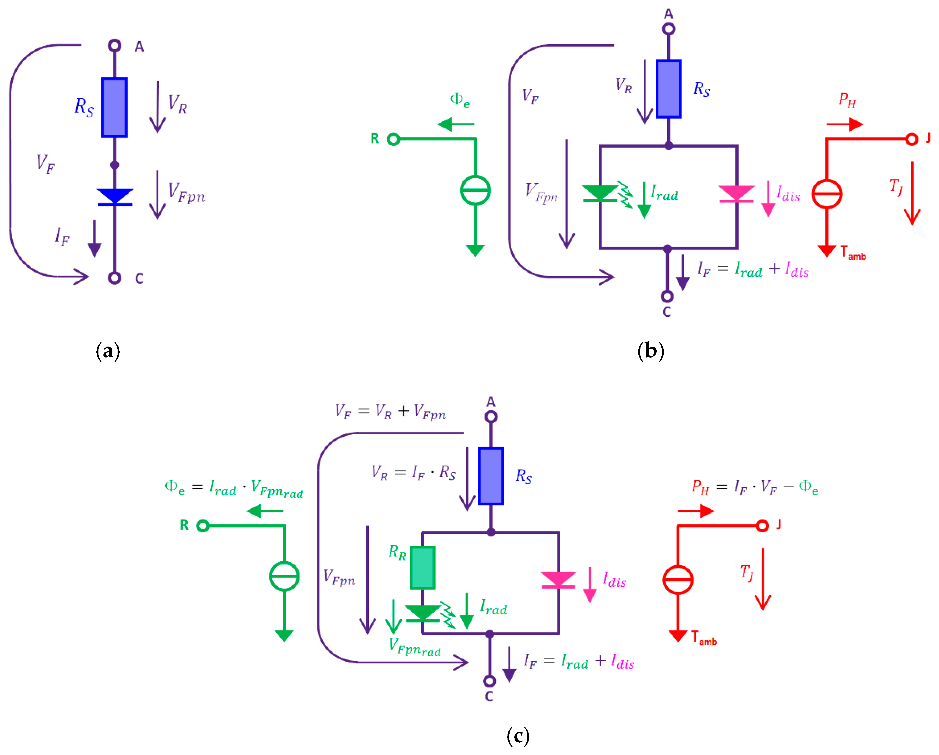
3.1. The Basic Concept: Splitting the Total Forward Current into Two Components

When we model an LED, we can split its forward current into two components [5], where in each current component, the charge carriers are subject to one type of recombination process only. This way we can distinguish between a current component associated with radiative recombination processes, denoted by I r a d , giving rise to light emission, and a current component associated with non-radiative recombination processes, denoted by I d i s , resulting in heat-dissipation at the pn-junction, as illustrated in Figure 5b. Both the radiative and the dissipative current components can be described by the Shockley equation [5].
The total emitted radiant flux, Φ e , leaves the device without adding to its heating. Accordingly, we calculate the heating power, P H , of the LED by subtracting the radiant flux from the supplied electrical power:
P H = I F · V F Φ e ,
as prescribed also in the JEDEC JESD51-51 standard [39].
In the model represented by Figure 5b, either the region around the peak efficacy or the high current range was modeled at better precision. This was resolved by inserting a series resistance, R R , in the “radiative branch” of the LED model as shown in Figure 5c [6,7].

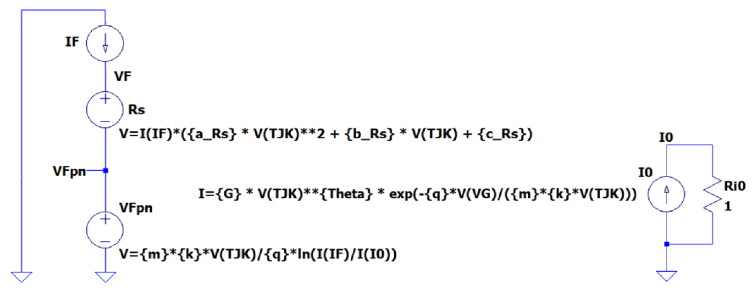
3.2. Model Equations at a Fixed Reference Temperature, T r e f , in the Current Driven Mode

With the insertion of R R , the model became an “implicit” one, and the currents and voltages cannot be expressed explicitly from I F . However, a circuit simulator with an iterative solver inherently handles this.
For the electric domain, the Kirchhoff equations depict the topology of Figure 5c. That is, the voltages of components in series must be totaled, and the I F current is split into I r a d and I d i s at the single internal node with a V F p n voltage. Regarding the branch equations, both diodes behave as dictated by Equation (2), with separate m r a d , I 0 r a d and m d i s , I 0 d i s parameters, respectively [5]. The emitted total radiant flux can be derived from the radiative branch:
V F p n = V F p n r a d + I r a d · R R = m r a d · V T · ln [ ( I r a d I 0 r a d ) + 1 ] + I r a d · R R ,
and:
Φ e = I r a d · V F p n r a d .
A further stage in the evolution of our model is that the I d i s component is no longer calculated, since through the use of Equations (2) and (3), an LED as a “diode” is described and Equations (10) and (11) yield the radiant flux. From this, and using Equation (9), the total dissipated power heating the LED is calculated. This present, new approach has the advantage that one can apply a simpler parameter extraction procedure than with the previous approaches [5], thus enabling the entire LED model to be based on the built-in models of a generic Spice circuit simulator.

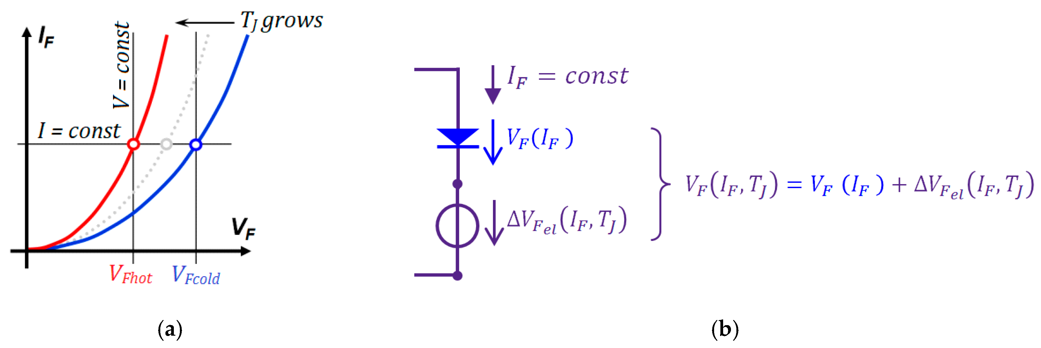
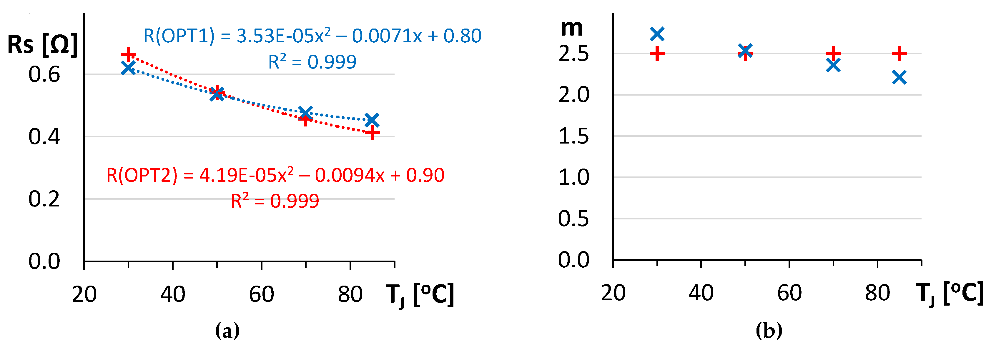
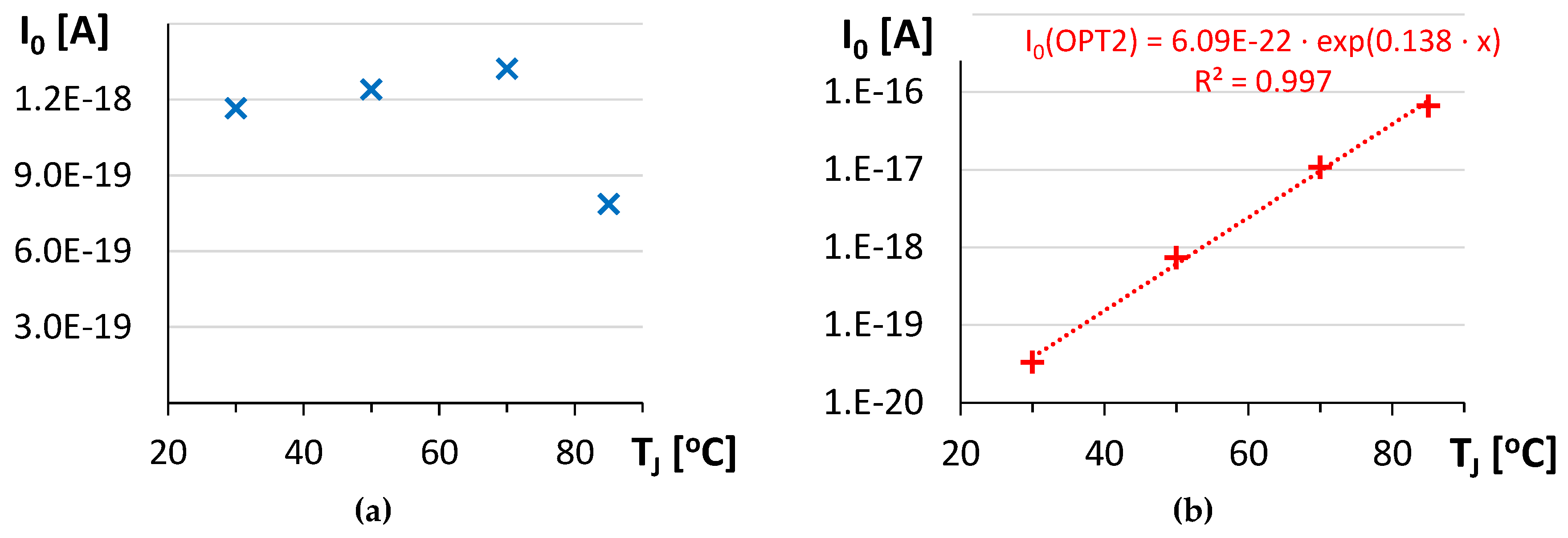
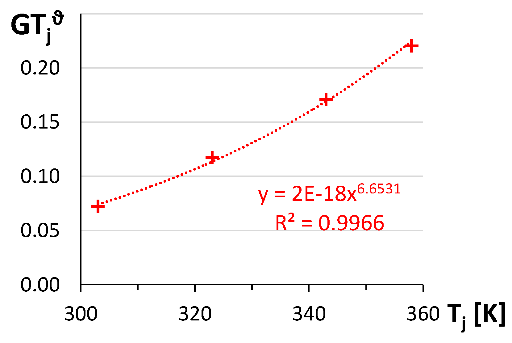
3.3. Implementation of the Temperature Dependence of the LED Chip Model

The second major evolutionary step in our LED chip multi-domain model is the way how the temperature dependences of the characteristics of an LED are modelled. Here, again, we consider the fact that in most applications, LEDs are driven by a constant DC forward current. In such a case, the electrical characteristics of the LEDs behave as illustrated in Figure 6a: The higher the junction temperature, the smaller the forward voltage drop is, when a constant forward current is forced through the LED. This can be understood by referring to Equation (5): The current coefficient, I 0 , appearing in Equation (1) exhibits roughly an exponential temperature dependence (resulting in approximately 15% growth by a centigrade at room temperature). With this dependence, if the total forward current, I F , is kept constant, Equation (1) can be satisfied only if the forward voltage across the diode shrinks as the junction temperature, T J , increases. For a single LED, this is typically 1 mV. Furthermore, a 2 mV degree change on top of the 2 V to 3 V forward voltage is represented by a simple linear relationship. However, for an accurate model, the use of a quadratic relationship is advised, as revealed by recent measurements of multiple LED types [40]. Thus, the entire LED can be modelled as a temperature independent diode with a temperature controlled voltage source, Δ V F e l , connected in series, where this voltage source represents the temperature induced change of the forward voltage.
In the complex model of Figure 5c, two resistors and two junctions are included. It would be impractical and hard to justify voluntarily distributing portions of the measured temperature related change of the entire LED to the four components.
It is more reasonable to start from a reference circuitry, fixing R S and R R at their value at T r e f , then adding diodes with V F 0 ( I F ) = V F ( I F , T r e f ) temperature independent equations (these can be easily implemented in a standard Spice macro model). After this, the temperature related variation of resistors and junctions can be cumulated into Δ V F e l and Δ V F r a d . sources (as illustrated in Figure 6b), approximated by a quadratic temperature dependence:
Δ V F e l = ( a e l · I F 2 + b e l · I F + c e l ) · ( T J 2 T r e f 2 ) + ( d e l · I F 2 + e e l · I F + f e l ) · ( T J T r e f ) ,
and:
Δ V F r a d = ( a r a d · I F 2 + b r a d · I F + c r a d ) · ( T J 2 T r e f 2 ) + ( d r a d · I F 2 + e r a d · I F + f r a d ) · ( T J T r e f ) .
These controlled sources can also be included in a Spice circuit macro model of an LED. This approach is similar to the approach used in a version of K. Górecki’s LED model presented in [28], except that in [28], the additional temperature controlled voltage source represents the extra voltage drop in the series resistance only, approximated by a simple linear temperature dependence. Our approach presented here has the advantage that the model of Δ V F e l can be directly derived from the results of the temperature calibration procedure required for the thermal testing of LEDs (as per the JEDEC JESD51-51 standard [39]).
With the above formula, for Δ V F r a d , the temperature dependence of the emitted radiant flux is calculated from the power of the radiative diode, as suggested earlier [5,6,7]:
Φ e = ( V F p n r a d + Δ V F r a d ) · I r a d .

3.4. Modelling the Emitted Luminous Flux

A major target for luminaire design is the total emitted luminous flux, Φ V , of an LED, which can be calculated from its emitted radiant flux, Φ e .
The emitted luminous flux, Φ V , of a light source is the quantity in which it is considered, how sensitive the human eye is to the emitted optical power at different wavelengths of the spectrum of the emitted light. This sensitivity is represented by the spectral luminous efficiency function, V ( λ ) . The ratio of the emitted total luminous flux and the emitted total radiant flux of a light source is thus characteristic of the spectral power distribution of the light source and is called the luminous efficacy of radiation [41], denoted by K . (The symbol of luminous efficacy of radiation is denoted by the capital letter Greek kappa that looks similar to the Latin letter K.) From the definition of K , it concludes that:
Φ V = Φ e · K .
In the case of LEDs, the forward current and junction temperature dependence of K (caused by the current and temperature induced changes of their spectral power distributions) can be accurately described by a bi-quadratic empirical model:
K ( I F , T J ) = ( a K a p · T J 2 + b K a p · T J + c K a p ) · I F 2 + ( d K a p · T J 2 + e K a p · T J + f K a p ) · I F + ( g K a p · T J 2 + h K a p · T J + i K a p ) .
In Table 1, an overview of the model parameters is shown. The extraction of the parameters occurs in a heuristic way. At low currents, the R S and R R resistors can be neglected, thus we can assume that V F = V F p n = V F p n r a d . I F is forced, thus it is known. The current component I r a d can be determined from a radiometric measurement, so the I d i s current component can be produced as a difference.
At a few low current points, the I 0 , m, I 0 r a d , and m r a d parameters can be calculated (similar to the way hinted later in in Figure 10). The series resistances can be derived from a few V F and Φ e points at higher currents. Iterative trials can be conducted to have a better fit in the lower or higher current range for the optical ports. A better fit can be achieved with a global optimization scheme for all parameters on all measured VF and Φ e points. However, with this mathematic apparatus, better accuracy can be achieved with the concept presented in Section 4.
A Spice implementation of the LED model (without the luminous flux model) is shown as the LTspice circuit schematics in Figure 7.

4. An LED Chip Multi-Domain Model Closer to Physics

The accuracy of the quasi-black box model (in terms of the radiant/luminous flux) for all the measured and modelled LED samples was good (within cca. 1%, as it will be shown later), but this accuracy was limited to about 1.5 decade of the forward current. Therefore, in order to better capture both sides of the maximum efficacy (shown in Figure 2), the range of this good fit had to be extended. In our quasi black-box model, a single ideality factor was assumed, while more realistic diode models use at least a second ideality factor for the regime of low forward currents. In the following subsections, the method of how our second multi-domain LED model was set up is presented. In our discussion, we rely on the basics of semiconductor physics that are detailed in well-known textbooks [37,38], also summarized in [42].

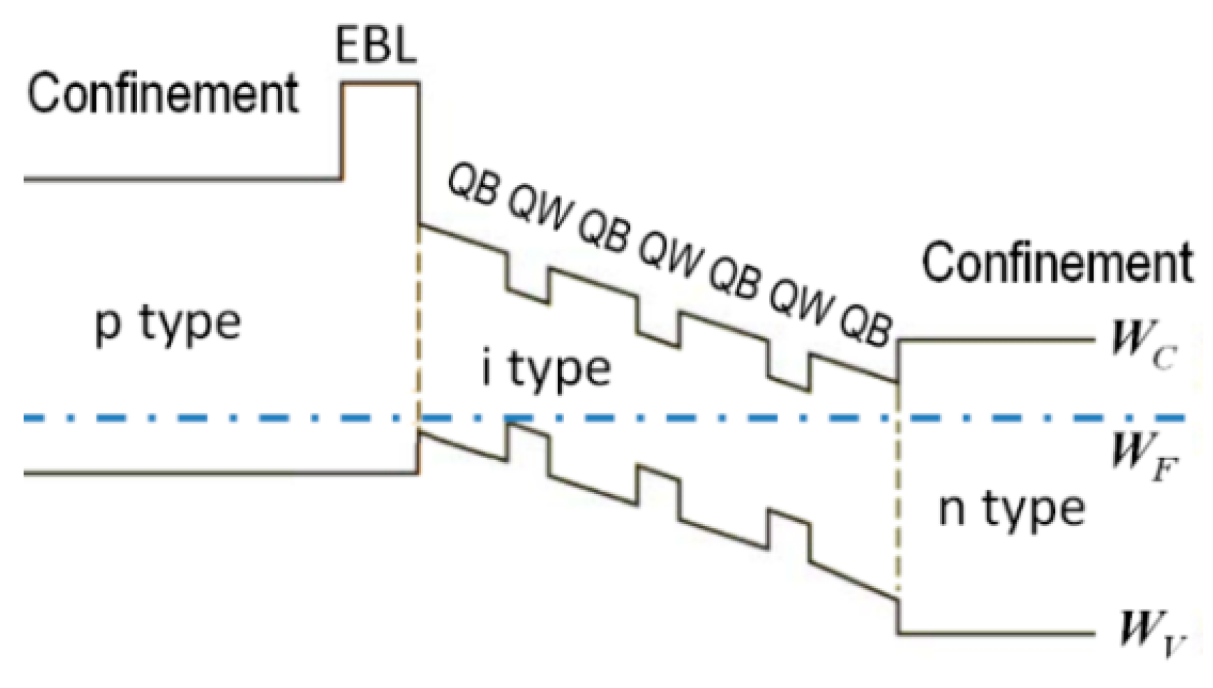
4.1. The Physical Roots

Up to date power LED devices approximately have the band diagram shown in Figure 8 (based on [38,43]). The active portion of the LED die consists of “bulky” p and n confinement layers, an electron blocking layer (EBL), and a sandwich of quantum barrier layers (QB) and quantum wells (QW). The bandgap in quantum wells defines the wavelength of the emitted light; a wider bandgap of the quantum barrier ensures low absorption of emitted photons and a high efficiency of the charge injection into the quantum wells.
In the stationary (DC) condition, the quantity of charge carriers in a material section is defined at a given temperature by the following factors:
  • Number of generated electrons/holes and their recombination through different mechanisms within the section. These effects can be thoroughly treated by the collision theory, but a simplified quantity called the generation and recombination rate can be used in the treatment of the statistical mechanics, too.
  • Injection from the adjacent sections, determined by the band structure near the interface.
The imbalance in these phenomena results in a current through all sections of the structure. The continuity equation from statistical mechanics dictates that this current is the same in all sections of the structure, but the actual carriers can be quite different. The exchange of the charge carriers occurs through generation and recombination effects. In the forward direction, the external driving force (voltage) diminishes the potential barriers in the band structure.
In “bulky” diodes, the diode characteristics in the forward direction can be calculated from the thermionic injection of the electrons confined in one side of the junction to the other similar side.
This injection is driven by the diffusion of charge carriers that have a higher energy than the potential barrier separating them from the adjacent material section. As the distribution of the carriers between energy levels is approximately exponential, when an applied forward voltage, V F , lowers the barrier, exponential growth in the diffusion current is experienced.
By solving the appropriate equations, one obtains a closed analytical formula under simplified conditions. These conditions are such that in the semiconductor material composed of adjoining ideal depleted and neutral zones, there is no particle generation and recombination in the depleted zone, and particles move until charge neutrality is reached in non-depleted zones.
The result is the well-known Shockley equation. By applying the forward voltage, V F , on the diode, the forward current, I F , is obtained as given in Equation (1), and reformatted for the forced forward current, I F , in Equation (2). In Equation (3), I F · R S describes the additional voltage drop on the diode. R S embodies the physical series resistance, but also some other effects, which do not follow the exponential equation.
The number of the movable particles quickly grows with the temperature. Solving the related equations of solid state physics, we can obtain that besides the thermal voltage, V T , introduced earlier, the I 0 parameter is also temperature dependent:
I 0 = G · T j ϑ · exp ( W g k · T j ) ,
where T j (with a lowercase j) denotes the junction temperature in Kelvins, and W g is the bandgap energy of the semiconductor introduced earlier. The coefficient, G , in Equation (17) and in further equations lumps appropriate constants that represent different material parameters. The value of ϑ for homojunctions is 3 (see, e.g., [37] or [42]). This equation is expressed in the same way as in Equation (5), but is now rewritten for an absolute T j junction temperature, instead of a temperature change around T r e f .
When a 3D zone faces a 2D well, a complex injection mechanism can be identified: Thermionic emission for the particles above a potential barrier, tunneling into and over the barrier below the barrier height, etc. These equations can be solved numerically [43,44], and the results can be approximated with a value of ϑ , as shown in Equation (17), that is significantly higher than 3.
By solving the equations of the charge distribution for several sections of the semiconductor, such as the depletion layer at the pn interface, quasi-neutral layers around the depletion layer, and the quantum wells, several equations can be obtained:
I F X ( V F ) = I 0 X · exp ( V F / ( m X · V T ) ) .
Some dominating effects can be treated with the collision theory, for more detail, see, e.g., in [38]. In the following paragraphs, these effects are summarized briefly.
A. Monomolecular recombination, where the electrons are recombined at irregularities of the crystalline structure, which are present in a steady number. Such centers of recombination can be dislocations, section boundaries, etc.
The recombination rate can be written as R = A · n , where A is the recombination probability and n is the electron density. The original Shockley-Read-Hall (SRH) recombination model treats the recombination at deep level traps in the band structure. The energy and momentum of the particle will be transferred to the partner in the recombination.
This kind of recombination produces current constituents of the I F A ( V F ) = I 0 A · exp ( V F / ( 2 V T ) ) style ( m A = 2 ), and becomes saturated at high particle concentrations. Accordingly, in models of bulky diodes, the depleted region where the particle concentration is low is taken into consideration.
B. Bimolecular recombination, where the electrons and holes participate in a band to band recombination, in the same section. The recombination rate can be written as R = B · n · p .
This kind of recombination adds I F B ( V F ) = I 0 B · exp ( V F / V T ) constituents ( m B = 1 ). The energy difference between the electron and the hole will be emitted as a photon.
C. Auger recombination, an electron and a hole recombine in a band-to-band transition and give off the resulting energy to another electron (or hole).
Three particles have to be present. The related recombination rate is R = C · n · n · p . The probability of this mechanism increases strongly with the carrier concentration.
The current component is not calculated as a closed analytic formula because at high carrier densities, the assumptions defined above do not apply, and the growth would be steeper than I F C ( V F ) = I 0 C · exp ( V F / V T ) .
In all models, the Auger constituents can be lumped into the I F · R S term as they appear at high forward currents.
In the forward direction, the generation of carriers in a section can be neglected.
Further effects with the treatment of statistical mechanics are:
  • Diffusion of minority carriers at low concentrations, that is, in low numbers compared to the density of the majority carriers. This yields I F d ( V F ) = I 0 d · exp ( V F / V T ) , corresponding to Equation (1) with m = 1 .
  • Diffusion of both types of carriers at high concentrations, when the quasi-neutrality principle makes the density of both carriers equal. This yields a current constituent in an I F q ( V F ) = I 0 q · exp ( V F / 2 V T ) form.
We can observe that all effects contributing to the junction current correspond to the general form of Equation (18), where m X is 1 or 2.
In the standard treatment of text books, disjoint locations in the structure are defined with dominant effects, which are then added up. As such, they claim the ln ( I F ) - ( V F ) chart shown in Figure 9a, with sharp slope breaks at the change of the current forwarding mechanisms. However, real diodes do not expose this alteration of the slope (Figure 9b), producing a continuous slope over several orders of magnitude.
At this point, the text books typically make a sloppy step, stating that an average ideality factor, m , can be used without too much further examination. A more established statement outlining a step to consider separate ideal depleted and neutral zones, and then to add up the currents belonging to disjoint zones is simple, but not true.
In reality, there is more than a zero charge in the depletion zone, the frontier of it to the p and n side is fuzzy, and charge neutrality is questionable. In the treatment of collision theory, instead of statistical mechanics, proportionality would be experienced among different charge movement mechanisms, and one mechanism would establish a particle surplus in a zone (e.g., injection), which enhances the probability of another mechanism (e.g., recombination). Until one such mechanism gets exhausted (for example, SRH recombination decays when deep level traps are mostly filled), a product of the mechanisms is observed:
I F ( V F ) = I 0 a · exp [ V F / ( m a · V T ) ] · I 0 b · exp [ V F / ( m b · V T ) ] · I 0 c · exp [ V F / ( m c · V T ) ] = I F · exp [ V F / ( m · V T ) ] ,
where I 0 = I 0 a · I 0 b · I 0 c · and 1 / m = 1 / m a + 1 / m b + 1 / m c + .

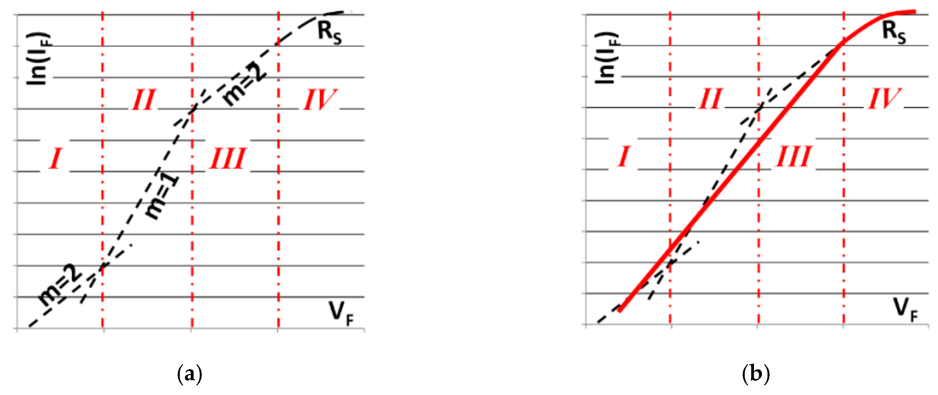
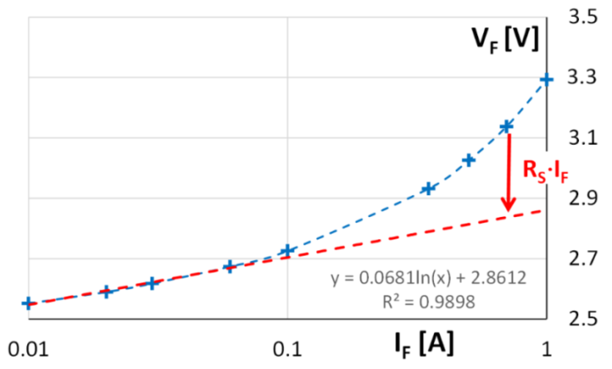
4.2. Modeling the Electrical Characteristics

By using the proportionality concept, verified by the measurements on many actual LED samples (with peak wavelengths chosen from different ranges of the visible range), m appears in Equation (17):
I 0 = G · T j ϑ · exp ( W g m · k · T j ) = G · T j ϑ · exp ( V g m · V T ) .
Figure 10 shows the measured V F of a royal blue power LED at several I F currents, from 10 mA to 1 A at a fixed T J = 85 °C. A Shockley type operation can be observed at low currents. At higher currents, the R S series resistance represents all losses which do not belong to the basic pn-junction operation.
Instead of just fitting a logarithmic trendline on a few points, the R S value in Equation (2) can be optimized such that the V R = I F · R S voltage at each measured I F is subtracted from the measured V F points (blue + markers) and the R S value which yields the best logarithmic fit on the V F V R relationship in the 10 mA to 1000 mA range is searched for. Herein, this optimization method is referred to as OPT1.
Applying OPT1 on the measured points, the curve of the V F p n = V F V R = C · ln ( I F ) + D format is obtained. The parameters, m and I 0 , of Equation (2) can be calculated from C and D as m = C / V T and I 0 = exp ( D / C ) , respectively.
Repeating the OPT1 procedure to all measured temperatures allows the temperature dependence of the parameters to be measured. First, the results of the method at various T J junction temperatures were demonstrated, on a royal blue LED (Cree’s XPE2 type).
The isothermal V F ( I F ) characteristics of the LED were recorded at a number of current values, between 1 mA and 1000 mA, at four different T J junction temperatures, namely at T J = 30, 50, 70, and 85 °C.
The blue x markers in Figure 11a show the fitted R S series resistance values generated by the OPT1 method at the given temperatures. The temperature dependence in this range is rather “flat”, so a good fit can be achieved by a second order polynomial approximation. For the model parameter, m , the optimization yields several values around m = 2.5 (the blue x markers in Figure 11b). Figure 12a presents the I 0 values for the best fit.
In Equation (2), the forward voltage, V F , depends on m · ln ( I 0 ) , and accordingly small numeric perturbations in the calculated m values can cause unacceptable scatter in the I 0 values, often several orders of magnitude. Supposing that the distribution among different carrier transport mechanisms does not change much in the temperature range modeled, the m value can be fixed.
A similar optimization algorithm denoted by OPT2 was also defined, where m is fixed, and the best (logarithmic) fit for R S is targeted again.
Applying OPT2 on the investigated XPE2 LED samples with m = 2.5 chosen, some accuracy of the fitting is lost, but the wild scatter of I 0 changes to demonstrate a reasonable trend (see the red + markers in Figure 11a,b, and Figure 12b).
The trend of I 0 in Figure 12b can be described by several mathematical formulae. The text books of solid state physics [37] offer several acceptable concepts.
The minimum expectation is that the formula should be valid in the relatively narrow temperature range of the measurement ( T j = 300 K to 360 K in absolute temperature).
The deduction in the related books can be found for the pn-junction in a bulk semiconductor, where ϑ = 3 / m . Thus, Equation (20) will be written in this case as:
I 0 = G · T j 3 / m · exp ( V g m · V T ) ,
and for a smaller range, Δ T j , the change around T j is:
d d T [ ln ( I 0 ) ] = 1 I 0 · d I 0 d T = 3 m · T j + V g m · T j · V T ,
resulting in the following ratio of the saturation currents at a Δ T j temperature shift:
I 02 I 01 exp [ ( 3 m · T j + V g m · T j · V T ) ] · Δ T j .
According to this, the I 0 current coefficient plotted in Figure 12b can be approximated by:
I 0 = I 01 · exp ( a · Δ T j ) ,
where I 01 = 6.09 × 10⁻²² and a = 0.138 in this particular example. The fit is correct in the given range with an R 2 determination coefficient of 0.9972.
A more ambitious attempt is through the direct use of Equation (20). By dividing the formula with the exponential part exp ( V g / ( m · V T ) ) , the following equation is obtained:
I 0 / exp ( q · V g m · k · T j ) = G · T j ϑ .
The OPT2 optimization process already yields I 0 at several temperatures, but to construct the left side of Equation (25), the values of the V g bandgap voltage are needed. As shown earlier by Equations (6) and (7), this can be calculated from the λ p e a k peak wavelength values obtained from the LEDs’ measured spectral power distributions. The temperature and current dependence of λ p e a k can also be taken into consideration, as presented, e.g., in [5].
In Figure 13, this “power of ϑ ” dependence of a royal blue XPE2 LED is illustrated, for which ϑ = 6.6531 was obtained with an R 2 determination coefficient of 0.9966.
Two optimization steps were conducted on the measured data of several LED devices of different colors (in this particular example: Members of Cree’s XPE2 family).
In Table 2, the measured λ p e a k values of these and the calculated bandgap voltages, V g , are listed. For the white devices, the peak wavelength of the blue part of their spectra was used.
In Table 3, the modeling parameters for all examined XPE2 devices are listed. To save space, only the minimum and maximum values of R S in the given temperature range are presented. In the tables, a color identification code is assigned to the LEDs, which is used below to denote them.

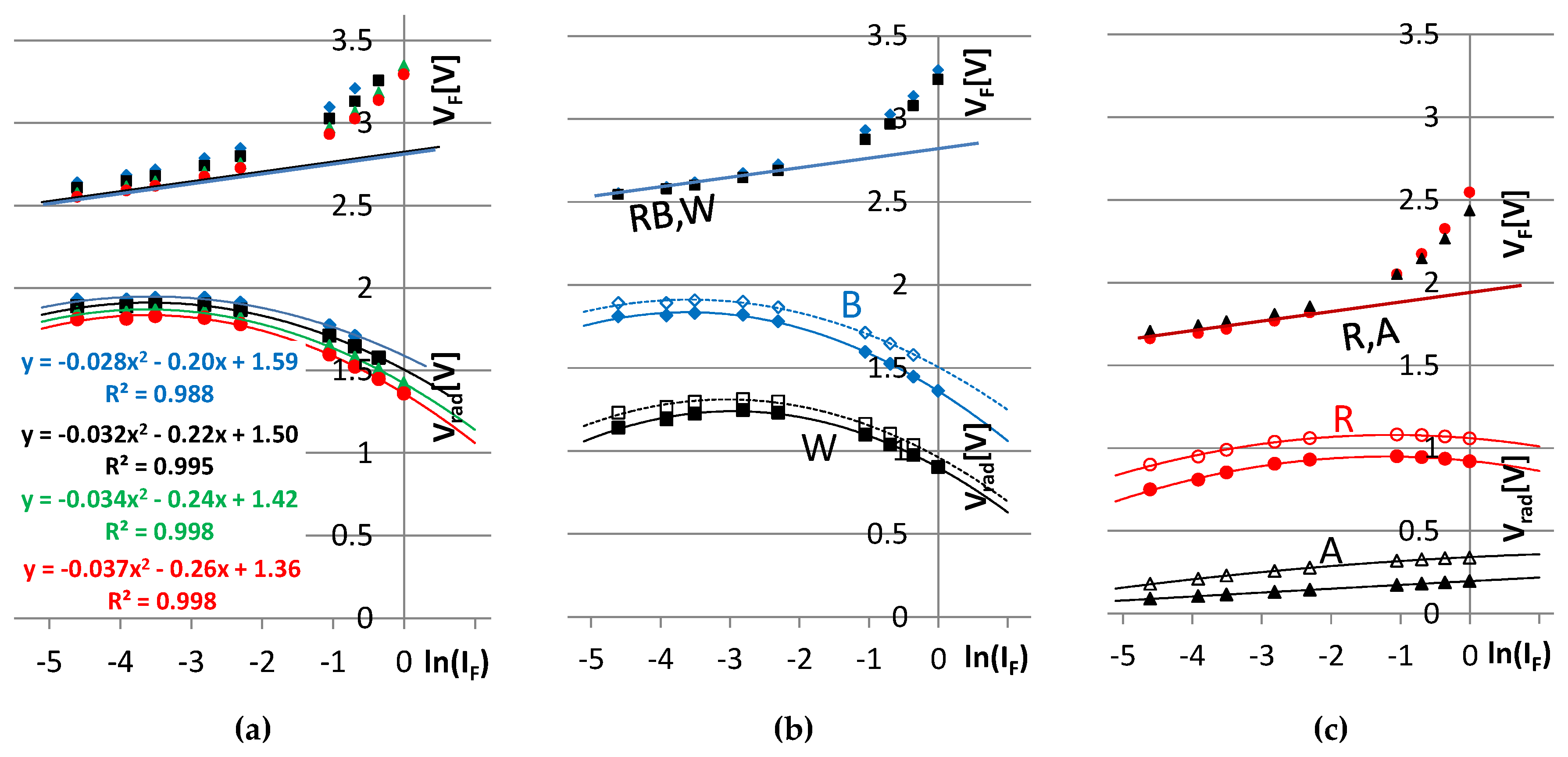
4.3. Modeling the Light Output Characteristics

In the previous subsection, an explicit model for the description of the LED behavior in the electric domain was created, i.e., the applied forward current, I F , directly determines the forward voltage, V F , using closed analytic formulae. Besides providing an improved method to capture the phenomena related to the carrier transport and recombination processes in LEDs’ active region, the use of explicit formulae is a clear advantage compared to the quasi black-box model described in Section 2, which requires that Equations (10) and (13) are solved iteratively (in the Spice circuit, macro implementations of the models of the circuit simulation algorithm are inherently iterative processes, so this difference between the two models is not relevant. However, in simulation environments, such as that depicted in Figure 4, avoiding internal iteration within the LED chip model is a clear advantage).
As hinted before, the optical domain is traditionally characterized by a bunch of current and temperature dependent parameters. The internal and external quantum efficiency ( IQE and EQE ) together yield the η e energy conversion efficiency also known as the radiant efficiency or wall plug efficiency ( η e = WPE = IQE · EQE ). Then, η e leads to the emitted total radiant flux, Φ e (also known as the emitted optical power), and the efficacy ( η V ) or the luminous efficacy of radiation ( K ) metrics lead to the emitted total luminous flux, Φ V . The chip level multi-domain LED model has to provide the Φ e and Φ V fluxes as output, therefore in the following, their modelling is provided.
Following the pattern of the calculation of the voltage drop of the “radiant diode” described in [5] (see also Figure 5), first, a new, virtual efficiency figure is introduced, which is called the radiant voltage:
V r a d = Φ e I F .
It will be later used in explicit models of the emitted total fluxes. The radiant voltage, V r a d , is tied to the energy conversion efficiency, η e , because η e = Φ e / ( I F · V F ) = V r a d / V F .
It must be noted that V r a d is merely a characterization tool, and ageing effects that degrade the external quantum efficiency, like graying of the lens, can significantly change it.
The measurements provided here prove that in a wide current range, where power LEDs are typically operated, V r a d can be approximated by a product of two Shockley style functions.
In the previous subsection, it was shown that a constant m parameter, over more orders of magnitude in current, expresses the proportionality between different charge transport mechanisms. Now, one blend of transport effects feeds the radiant recombination by injecting carriers into the quantum well, while other effects (such as the Auger recombination that enhances electron leakage over the electron blocking layer) deport the carriers before they can recombine. Detailed numeric analysis of the actual material compositions and geometries is broadly treated in the literature, like [43] or [44].
By maintaining the concept of proportionality that is underpinned by constant m in the forward current range of interest, whether the measurements support a:
V r a d = [ a · ln ( I F / I 0 a ) ] · [ b · ln ( I F / I 0 b ) ] ,
type formula can be checked. The introduction of the notation, z = ln ( I F ) , c = ln ( I 0 a ) , d = ln ( I 0 b ) , allows Equation (27) to be rewritten as follows:
V r a d = a · b · ( z c ) · ( z d ) = a b · ( z 2 z c z d + c d ) ,
which can be further simplified to:
V r a d = A z 2 + B z + C .
Figure 14 shows the V F and V r a d values of the royal blue and phosphor converted white LEDs measured at different junction temperatures. It was found that the fitting of a quadratic polynomial with A , B , and C coefficients corresponding to Equation (29) obtained an excellent match on the 10 mA to 1000 mA region of the I F total forward current, with an R 2 determination coefficient of around 0.99.
The η e energy conversion efficiency can be gained by dividing the V r a d values with the V F forward voltage, which is also shown in the diagrams of Figure 14. This way, through V r a d , an explicit forward current dependent model for the radiant flux is given: Φ e = V r a d · I F .
Figure 14a,b show the quadratic fit on ln ( I F ) for the royal blue and white devices, while Figure 14c shows the same for the red and amber devices.
The charts in Figure 15 present the temperature related changes of the A , B , and C parameters used in Equation (29), for all colors. The temperature dependence is rather flat again; it was found that a second order polynomial can be fitted at R 2 > 0.99.

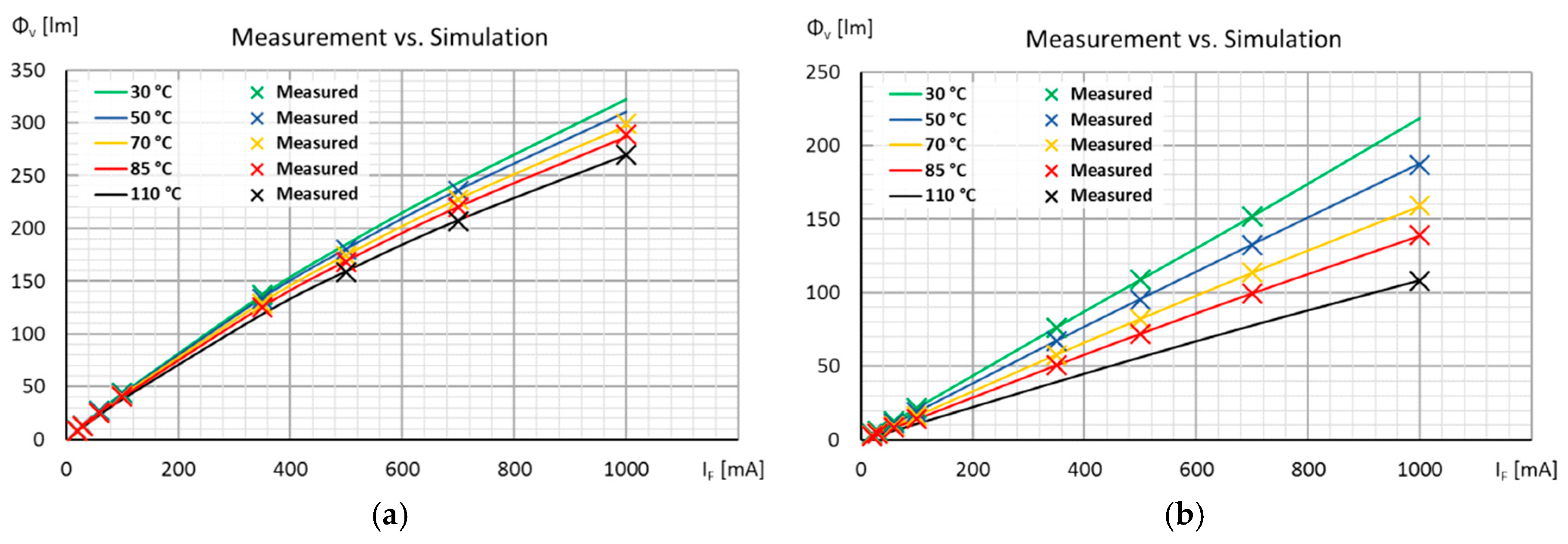
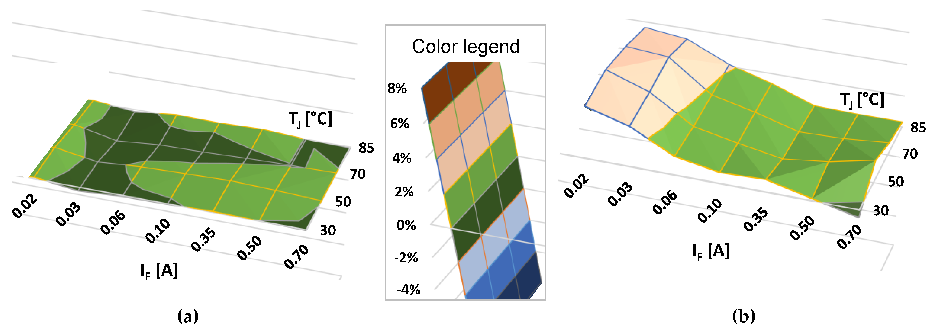
4.4. The Predictive Power of the Physics Based Model

To prove that the models defined so far describe the electrical and optical domain in the current and temperature range of interest accurately the Cree XPE2 power LED family was characterized. All measurements were done in a combined thermal transient and optical measurement arrangement [34] that complies with CIE’s and JEDEC’s recent recommendations and standards on the optical and thermal testing of power LEDs [32,39,45].
Five different color LED types were measured, using multiple numbers of samples from each type. To make the modelling easier, the cold plate control mode was set to regulate towards a fixed T J junction temperature as described in [31]. This ensured that the measured DC characteristics and the radiometric and photometric values corresponded exactly to the thermal boundary of a constant T J , without further model correcting steps. Current levels were selected between 20 mA and 1 A, and T J temperatures ranged from 30 to 85 °C.
In order to demonstrate the predictive power of the modeling concept, the red devices from Table 2 were selected because their η e radiant efficiency has the largest temperature and current dependence (Figure 16b). Still, it is expected that the model extracted from a single median device accurately represents the devices in the measured binning class. (The median device is the LED sample, which is closest in terms of one if its selected parameters to the median value of the distribution of that parameter obtained for the entire LED population)
The electrical model of red LEDs was characterized by just a few parameters in the previous subsection. The R S values were approximated by a parabolic function with values around 0.7 Ω, m was set to 1.5, and for the “power of ϑ ” dependence of the I 0 saturation, ϑ = 6.59 with an R 2 of 0.99 was obtained.
Selecting the LED of median V F value from the bin, the I F V F plots at four T J temperatures were measured as shown in Figure 16a.
In Figure 17a, a 3D plot of the relative error of the modeled V F forward voltage is shown. The chart compares the calculated forward voltage, V F , from the Shockley model of the median device to its own measured values from Figure 16a. The accuracy of the model is within ±0.5% on the whole current and temperature range.
The figure and also the subsequent similar figures show the 20 mA to 700 mA range, in which all T J values were reached. The colors correspond to a ±4% range of error in the figures, representing an error of V F and a ±8% range showing the error of Φ e .
A “worst case” situation is shown in Figure 17b. Here, the measured forward voltage of the device which has the lowest VF is compared to the model based on the median device. Still, the error remains in the 0% to 2% range.
In Figure 18 the modeled Φ e radiant flux of the “median V F ” red sample to the measured Φ e of the “median V F ” sample itself (Figure 18a) and to the measured Φ e of the “lowest V F ” sample (Figure 18b) is compared. Again, the self-modeling is accurate to 1%, the scatter between samples is higher, and the Φ e radiant flux of the least similar sample deviates a few percent from the median device.
The test was also carried out on royal blue and phosphor converted white samples, composed of a similar royal blue chip and a yellow phosphor layer. It was found that the V F scatter was very low—obviously the same as in the case of the royal blue devices—and the “median” white LED modeled its own radiant flux within 1% (Figure 19).
However, the white sample of the lowest V F showed up to a −8% to +18% difference of Φ e in the 30 mA to 1000 mA forward current range. This may have occurred due to the larger scatter in the phosphor quality and also indicates that the binning was performed at a single ( I F _ b i n , T J _ b i n ) operating point (Figure 20).
This finding corresponds to the results of the variability analysis of the thermal properties of the blue and white LED samples [46,47], where a significantly larger scatter of the properties of the white samples was found.

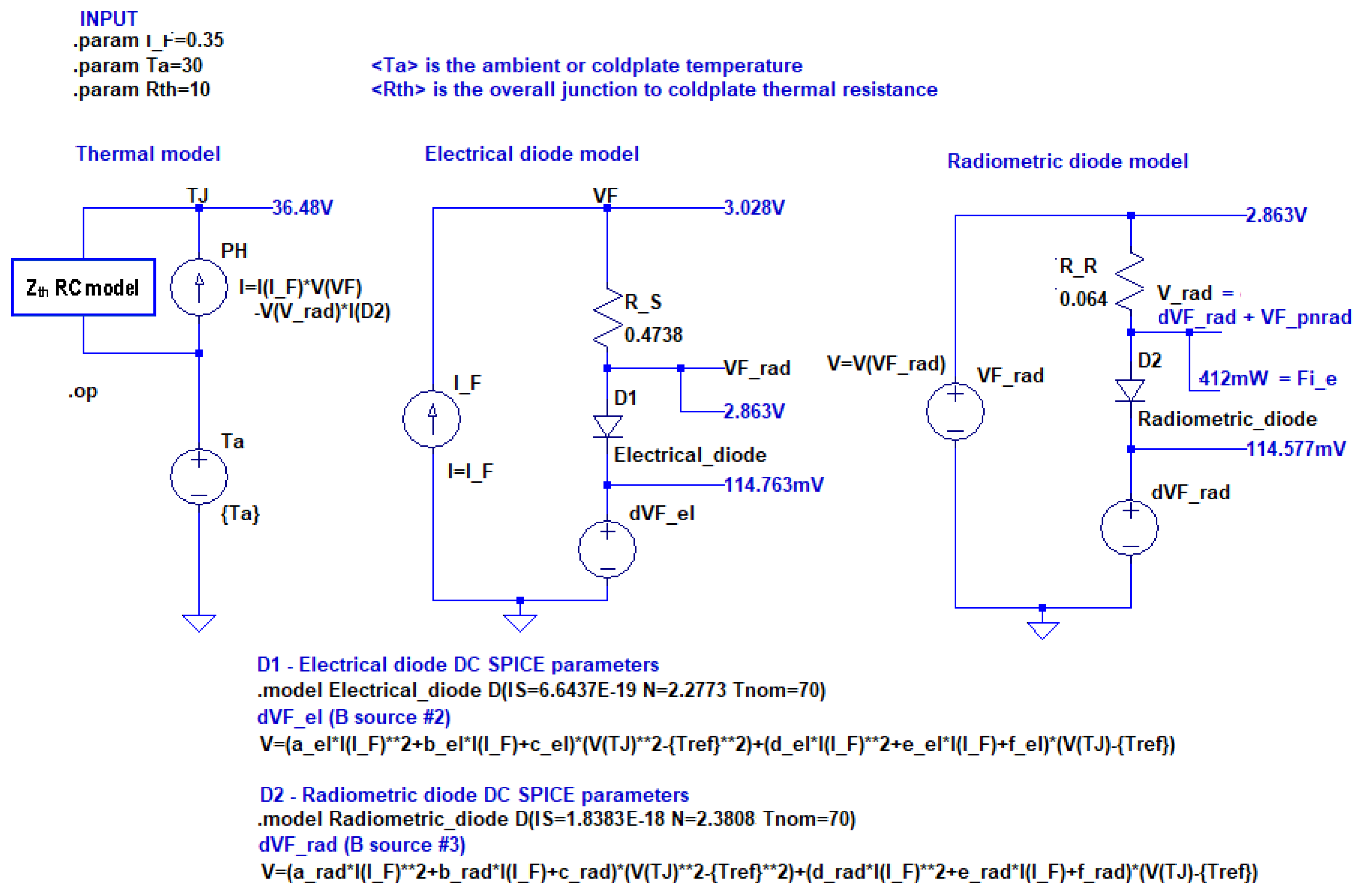
4.5. The Actual Implementation of the Physics Based Model

The physics based model differs from the ones hardcoded in all Spice program versions for semiconductor diodes. Therefore, a circuit macro in visual basic was created in which the controlled voltage or current sources directly represent the model equations.
It must be emphasized that this model is based on explicit formulae; I F and T J yield all output data directly, without internal iterations as implied by the circuit scheme in Figure 5c.
The I F V F relationship in this model is coded as Equation (2). The R S series resistance has the quadratic temperature dependence of Equation (4), as justified in Figure 11a. The temperature dependent I 0 saturation current was calculated based on Equation (20).
In all equations, the V T thermal voltage and the V g bandgap voltage were calculated for the actual T j junction temperature (given in Kelvins). In the bandgap voltage formula, the peak wavelength was approximated by a relationship derived from Equations (7) and (8) for values of T j close to 300 K:
λ p e a k = L p 1 · T j 2 + L p 2 .
The emitted total radiant flux (optical power) was calculated with:
P o p t = Φ e = V r a d · I F .
As supported by Figure 15, the modest change in the temperature dependence of V r a d can be reflected by quadratic tuning equations:
V r a d = ( a _ A · T J 2 + b _ A · T J + c _ A ) · ( ln I F ) 2 + + ( a _ B · T J 2 + b _ B · T J + c _ B ) · ( ln I F ) + + ( a _ C · T J 2 + b _ C · T J + c _ C ) .
The heating power was calculated again, like in the quasi black-box model, using Equation (9). All the coefficients in these equations are model parameters that must be identified for a given LED type, given now by the systematic methodology of subsequent OPT1 and OPT2 operations.
For the Φ V luminous flux, several approaches were tested, such as deriving it from Φ e through the fitting of polynomials or searching for a polynomial on the raw I F . Finally, it was found that best fidelity over a wide current range can be achieved with a polynomial on ln I F , Which was calculated similarly to Equation (32), with a different set of constants.
A Spice implementation of the proposed new model was created. A part of it representing the electrical characteristics by controlled sources is shown in Figure 21.
The T J junction temperature can be computed by inserting the thermal model of the packaged LED into the thermal model of the environment. These models are deeply treated in [7,48].
A simple Foster-style equivalent thermal chain representing the device and the outer world is shown in Figure 22. The conversion from the T J junction temperature in Celsius to T j in Kelvin yields the TJK “voltage” for the model calculations in Figure 21.
In Figure 23, the response of a blue XPE2 LED from Cree is monitored in its thermal environment represented by the simple compact thermal model. First, heating can be observed. The current grows linearly from 10 mA to 1 A in the first 1 μs (the current was multiplied by 10 in order to make it visible in the chart. The curvature corresponds to linear growth in the log-lin scale).
In the further two seconds, the increase of the temperature (25 to 70 °C) and the decay of the forward voltage and radiant flux can be observed. The “bumps” of the curves correspond to the thermal time constants in Figure 22, τ 1 = 1 ms, τ 2 = 100 ms.

5. Multi-Domain Modelling of LEDs for Real Design Tasks

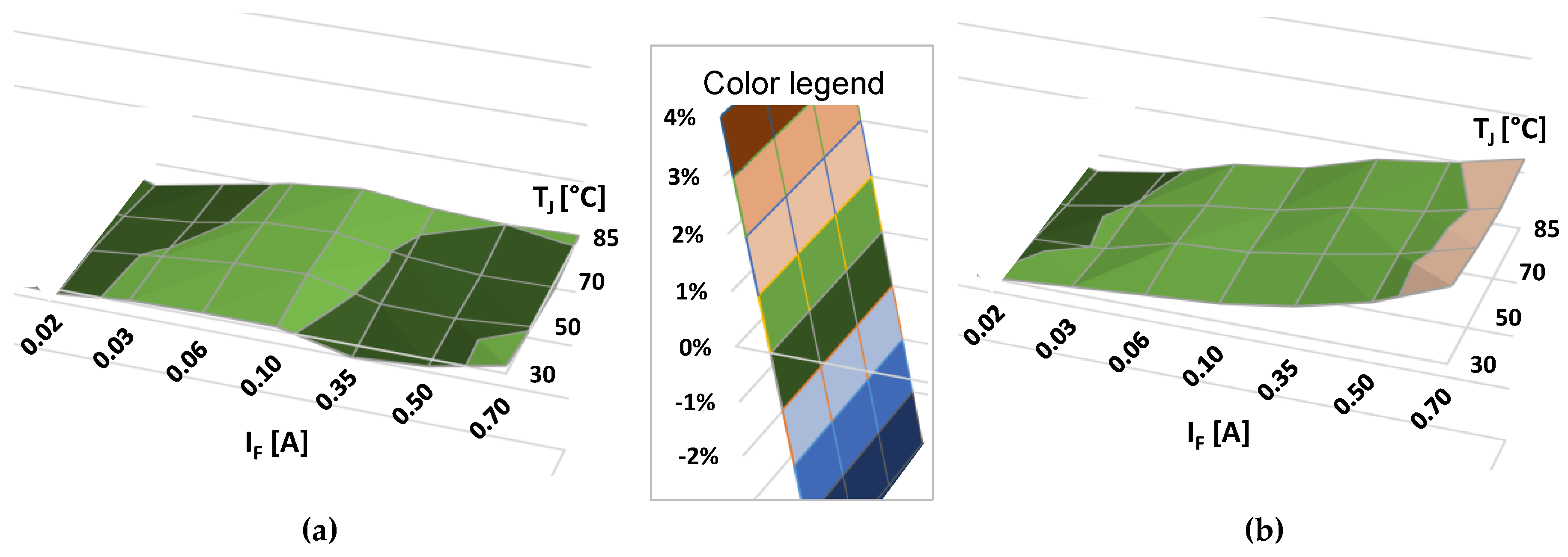
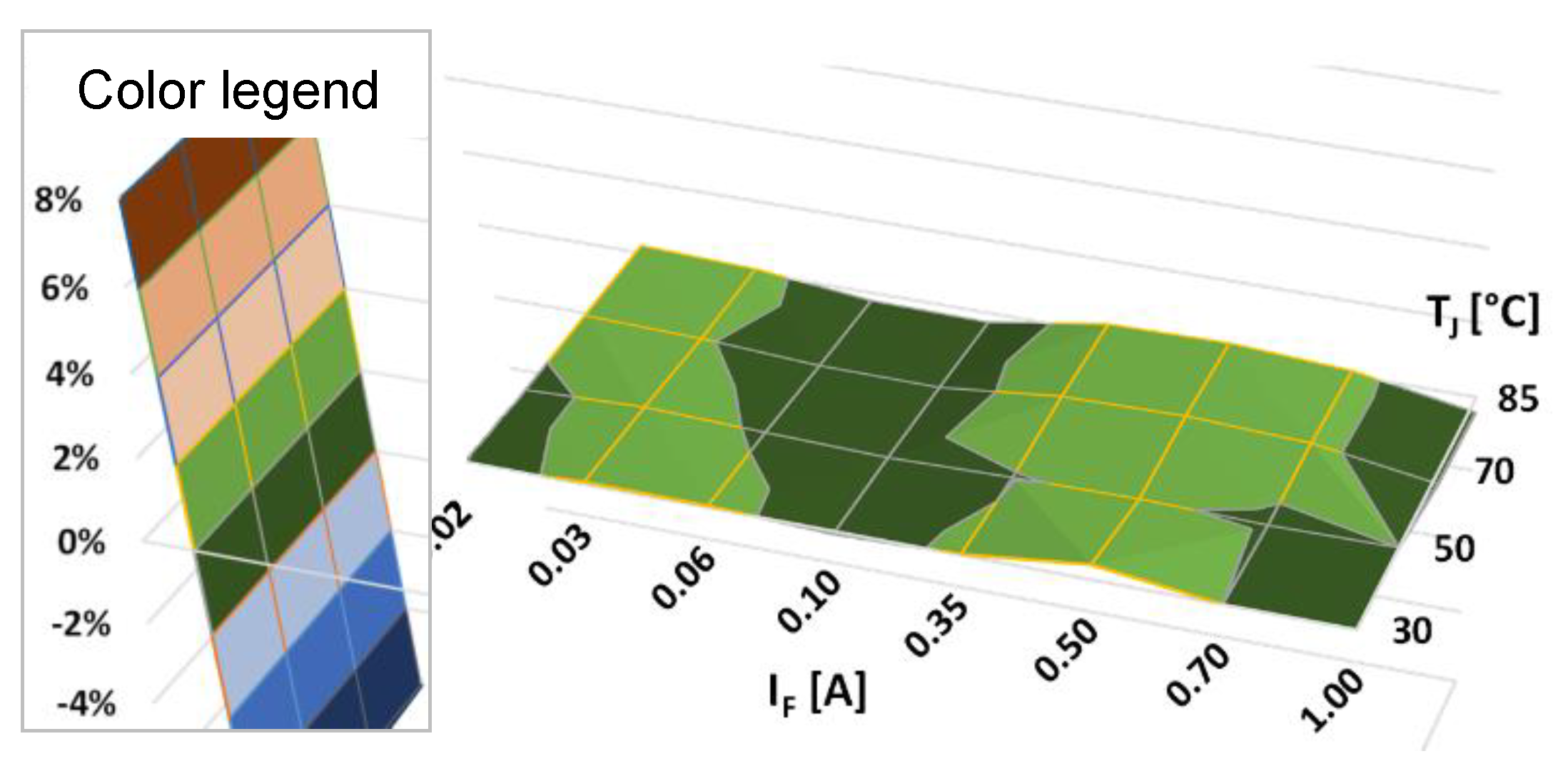
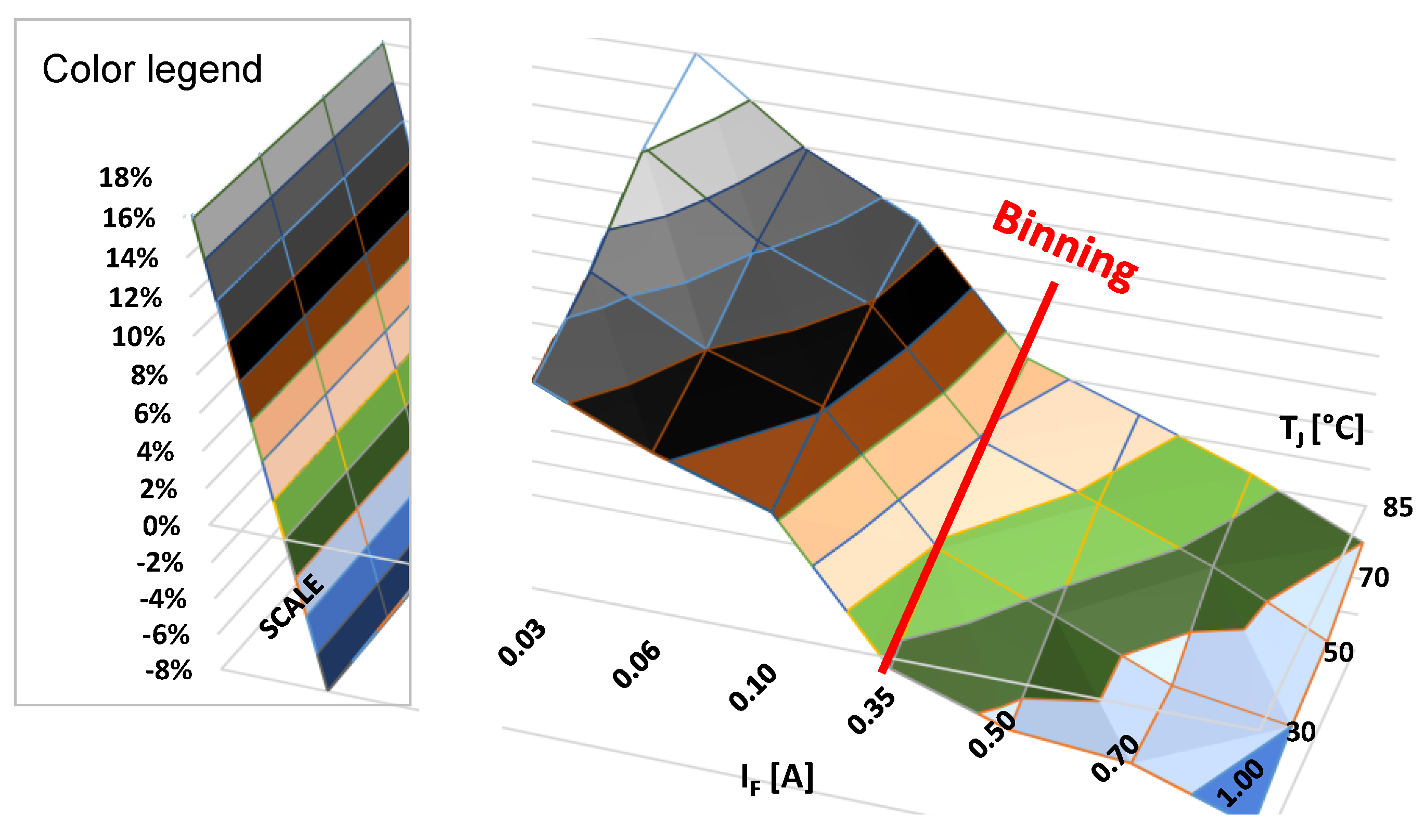
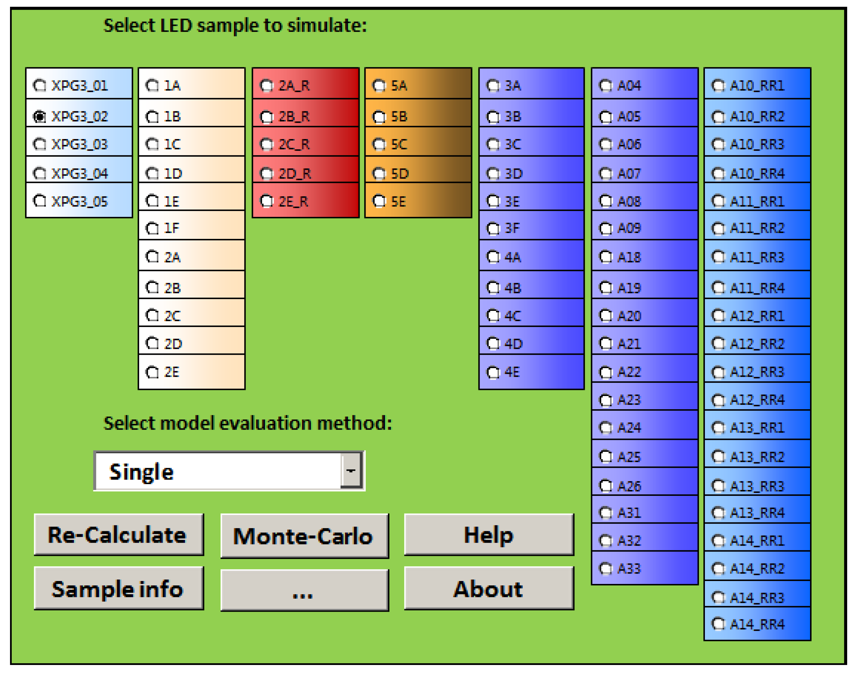
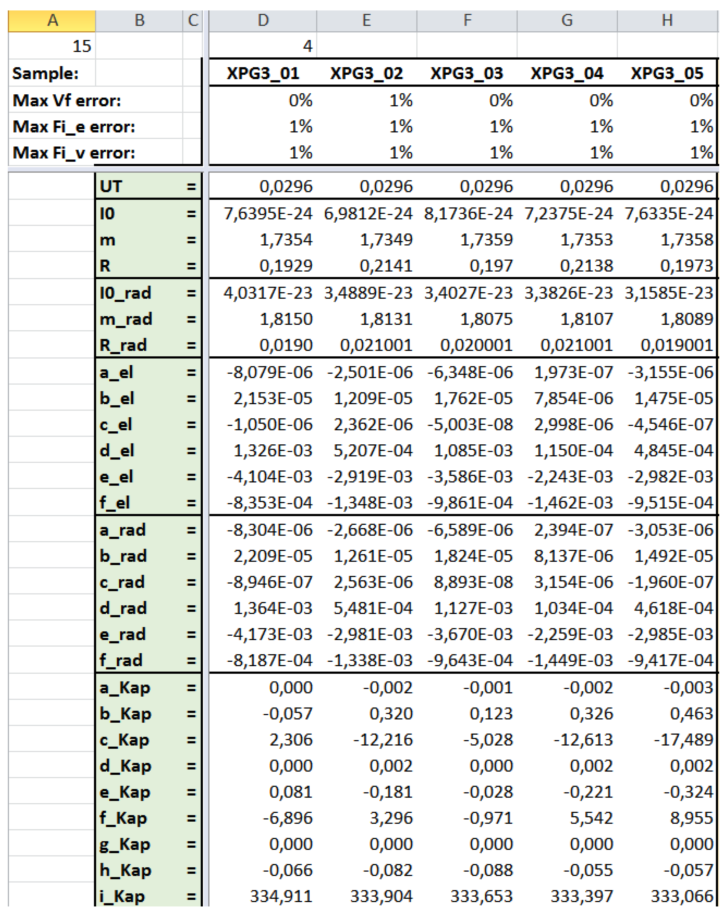
5.1. Modeling an “LED type” and Parameter Extraction

Several approaches to represent an “LED type” based on the measurement results obtained for a given LED population exist. As mentioned earlier, in the Delphi4LED project, a specific task was devoted to study the sample-to-sample variations of LEDs and provide statistical models to describe these variations. Within this work, the properties of the junction-to-ambient heat-flow path of LED populations were investigated. The analysis was done on 11 royal blue and 10 phosphor converted white LEDs [46,47,49].
As one of the results of this study, the concept of the “median device” was established. The sample with a mechanical assembly providing the thermal resistance closest to the average of the entire population was selected as the “median device”. The properties of the median device with their mean values and distributions are characteristic of the “LED type”.
In terms of the IVL characteristics, nominating a median device is less straightforward [49]. In the study of the predictive power of the physics based multi-domain LED model, the median device was the one with an electrical characteristic closest to the average characteristic.
Another option is to use a combined metric, which lumps the “diode” property and the “light source” property of an LED. Such a metric could be the η e energy conversion efficiency or the η V efficacy. The “median device” could be the one which has an η e ( I F , T J ) efficiency or η V ( I F , T J ) efficacy surface closest to the average surface. Elaboration of the right method for identification of the “median” LED is still an ongoing activity. Some results obtained so far are reported elsewhere [49].
For demonstration purposes, however, a model parameter set for the measured LED populations was established, see Figure 24. In relation to the quasi black-box model presented in Section 2, a total of 75 LED samples of six different types were characterized in 35 operating points (the minimal number of operating points for the measurement of LEDs’ isothermal IVL characteristics was defined in a round-robin test performed at the beginning of the project [34]). A global parameter fitting procedure was performed on all the individual measurement sets. The parameter sets obtained in this way represented the individual LED samples, rather than the given “LED type” or “bin of the LED type” to which the samples belonged to.
Then two average models for each LED type were set up with the intent to model the “LED type” instead of the individual samples: One by averaging the resulted model parameters of the same LED type and another one by averaging the corresponding measurement results first and performing the fitting procedure afterwards.
As an example, out of the 75 LED samples of six different LED types, Figure 25 compares the measured and modelled luminous flux values of a phosphor converted white and red high power LED sample, as a function of the forward current and junction temperature. The complete set of parameters and fitting errors in terms of the forward voltage and emitted fluxes obtained for five samples of white LEDs is shown in Figure 26.
XPG3 white LEDs from Cree were used as a device demonstrator in the project. As an ultimate proven method for the obtainment of a model parameter set with statistical models of their distributions was lacking, the above mentioned averaging of the measured characteristics was applied before the actual parameter fitting procedure.

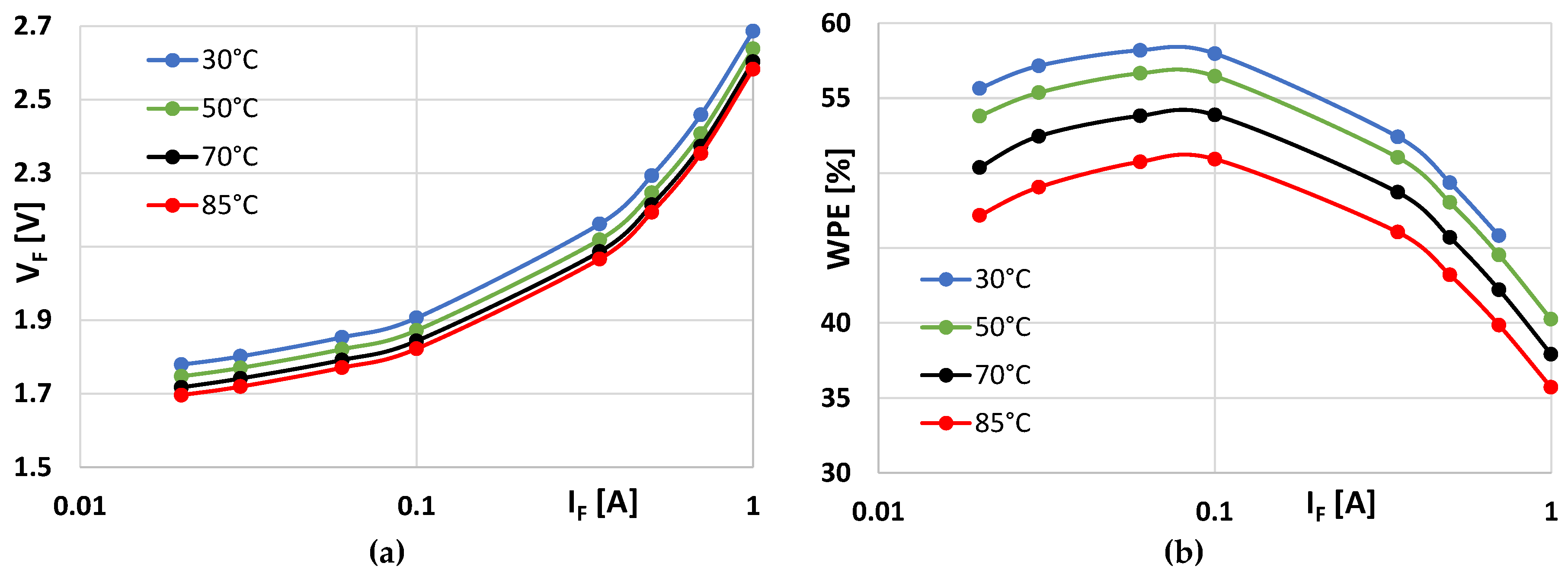
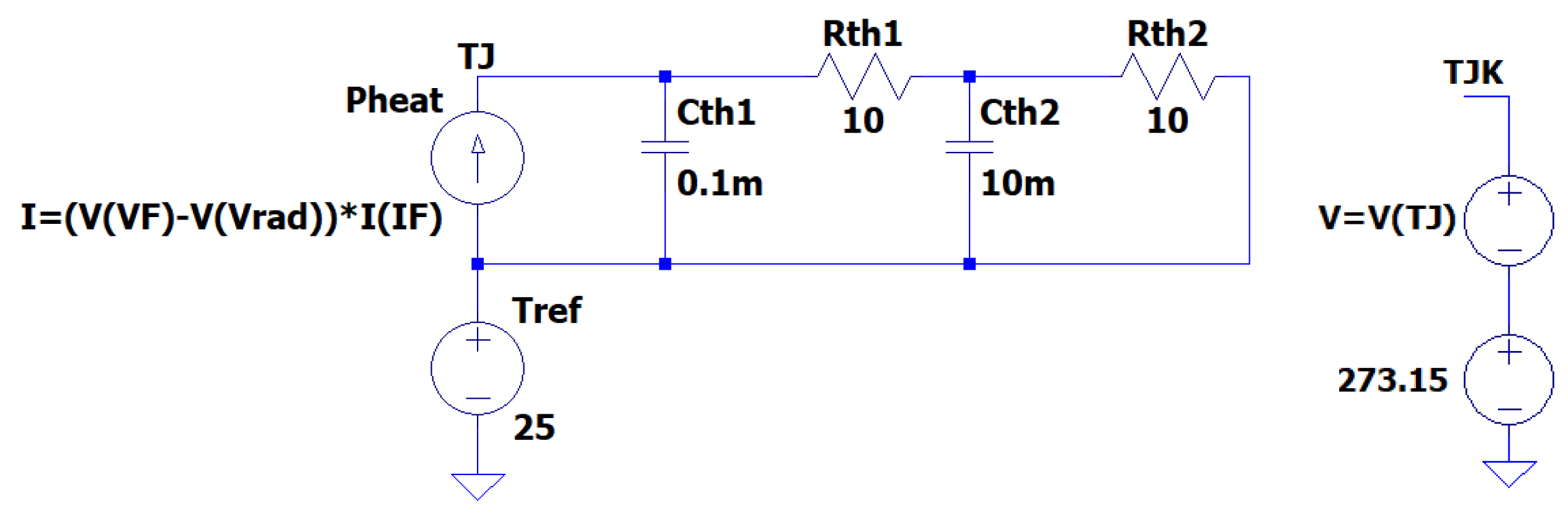
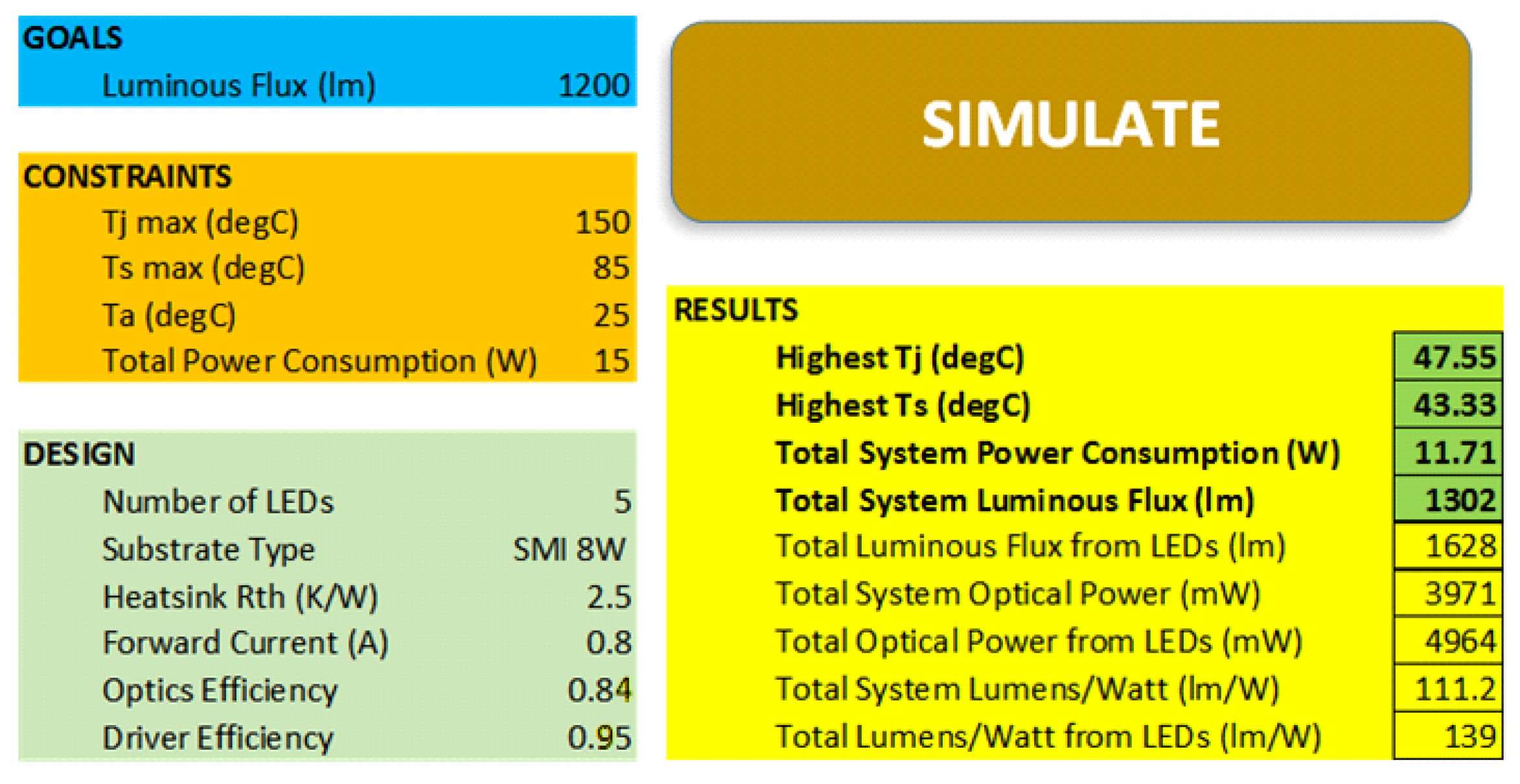
5.2. Applying the Quasi Black-Box Model for a Real Luminaire Design Task

The same set of visual basic macros that were used for parameter identification were also built into a spreadsheet application based on the LED luminaire design calculator [3]. This way the model applied to Cree XPG3 LEDs was used in two implementations of the foreseen Delphi4LED design processes [3,4] to predict the performance of different versions of an “outdoor 10 W LED spot” type luminaire used as the first project demonstrator.
The luminaire design calculator is equipped with a simple user interface, as shown in Figure 27. The designer has to provide the major lighting design goal in terms of the total emitted luminous flux of the luminaire and has to provide the design constraints, such as the maximum allowed temperatures and maximum total electrical input power. The third group of input parameters describes the major properties of a foreseen luminaire design variant, such as the total number of LEDs (in a series electrical configuration) to be used in the luminaire, foreseen input electric current (the common I F forward current of the LED string), driver and optics efficiencies, and the choice of the LED module substrate and luminaire heatsink.
Once all these inputs are provided, the spreadsheet application creates the compact thermal model of the LEDs’ 3D environment and calculates the LEDs’ operating points corresponding to the specified ambient temperature and forward current through a relaxation type iterative solution process as illustrated in Figure 4.
In Figure 27, the calculated results for the SME-version of the first project demonstrator, the “10 W outdoor LED spot”, are shown. The prototype of the luminaire has also been manufactured with the chosen number of LEDs, substrate material, layout arrangement, and heatsink.
At an independent testing laboratory, good agreement between the measured and simulated major operating parameters was found, as shown in Table 4. In terms of the total emitted luminous flux, the mismatch between the simulated and measured value was cca. 2.7% while in the case of the total input electric power, the mismatch was cca. 8%. Considering the fact that the luminaire design calculator uses a rough thermal model of the luminaire as a heat-sink, these results are satisfactory. Work is ongoing for the application of a second, physics related multi-domain LED model to other demonstrator systems of the project.

6. Conclusions

In this paper, we first presented an implementation of the latest version of the improved chip level multi-domain LED model proposed earlier for the Delphi4LED project [6,7] as a quasi black-box model of LEDs. This model was based on formulae widely used in textbooks and built-in diode models of the Spice-like circuit simulator. We also presented a new multi-domain LED model, closer to the physics of LED operation. Both models were implemented in the form of visual basic macros and as circuit models suitable for usual “electrical only” Spice circuit simulators. In the Spice implementations, crucial elements are the different controlled sources, which allowed us to directly represent our model equations.
Both models were included in a spreadsheet application to support the design of different demonstrator luminaires of the Delphi4LED project and both models were also tested with simple LTspice simulation case studies.
The advantage of the quasi black-box model is that it can be considered as an extension of LED vendors’ present Spice models of LEDs, thus, from a user’s perspective, they can be used in a similar way, with a Spice solver, to the current existing Spice models of LEDs. This model calculates the luminous flux from the radiant flux, using an empirical model of the efficacy of radiation of LEDs. The disadvantage of this model is that for forward currents below the current where the efficacy peak occurs, it overestimates the light output. Another possible disadvantage of this model is that one of its equations is an implicit one, requiring the model to perform internal iterations. In the case of the design complexities encountered in the Delphi4LED project demonstrators, however, this did not result in unacceptable response times of the Excel spreadsheet application in which the model was used.
Our new proposed model, more closely related to the actual physics of the operation of modern power LEDs, is largely different from the usual textbook models. Therefore, the Spice implementation of this model cannot rely on the standard built-in models of semiconductor diodes. The major advantage of this model is that it solely uses explicit formulae to describe both the electrical and light output characteristics of LEDs. This model calculates the luminous flux directly from the forward current and the junction temperature.
Unlike the previous academic versions of Spice models for LEDs, with the present implementations of our new chip level multi-domain LED models, we targeted real life, industrial design flows aimed at LED luminaire design, such as that proposed by the Delphi4LED project. An important aspect of our approach is the strictly modular, hierarchical modelling, according to which the chip level behavior of LEDs is completely separated from the compact model of the chips’ thermal environment, thus even the compact thermal models of the LED packages are external to our proposed chip level LED multi-domain models.
LED modeling is not finished here. A couple of issues still must be dealt with, such as the necessary number of LED samples to be characterized for the extraction of the parameter set that is representative of the given LED type; how to represent the sample-to-sample variations of the model parameters; how to include typical LED product parameters, such as the binning value of the forward voltage, etc. These are questions that are still the subject of research within the Delphi4LED project [49].

Author Contributions

Conceptualization, A.P. and G.F.; Data curation, L.G., G.H. and J.H.; Formal analysis, A.P., G.F. and M.R.; Funding acquisition, A.P.; Investigation, G.F., L.G., G.H. and J.H.; Methodology, L.G., G.H. and J.H.; Project administration, A.P. and M.R.; Software, L.G., G.H. and J.H.; Supervision, A.P. and M.R.; Writing—original draft, A.P., G.F., G.H. and J.H.; Writing—review and editing, A.P., G.F. and M.R.

Funding

This research received funding from the European Union’s Horizon 2020 research and innovation program through the H2020 ECSEL project Delphi4LED (grant agreement 692465). Co-financing of the Delphi4LED project by the Hungarian government through the NEMZ_16-1-2017-0002 grant of the National Research, Development and Innovation Fund is also acknowledged. The modelling work of LEDs performed at BME was also funded by the K 128315 grant of the National Research, Development and Innovation Fund and was also supported by the Higher Education Excellence Program of the Ministry of Human Capacities in the frame of Artificial Intelligence research area of Budapest University of Technology and Economics (BME FIKP-MI/SC).

Acknowledgments

Support from Delphi4LED project partners, especially from G. Martin (Signify), Ch. Marty (Ingelux), R. Bornoff (Mentor, a Siemens business), D. Fournier (PISEO) and E. Morard (Ecce’lectro) is acknowledged.

Conflicts of Interest

The authors declare no conflict of interest. The funders had no role in the design of the study; in the collection, analyses, or interpretation of data; in the writing of the manuscript, or in the decision to publish the results.

References

  1. Martin, G.; Poppe, A.; Lungten, S.; Heikkinen, V.; Yu, J.; Rencz, M.; Bornoff, R. Delphi4LED—From measurements to standardized multi-domain compact models of light emitting diodes (LED). Electronics Cooling Magazine, 4 August 2017; 20–23. [Google Scholar]
  2. Delphi4LED Project Website. Available online: https://delphi4led.org (accessed on 27 March 2019).
  3. Marty, C.; Yu, J.; Martin, G.; Bornoff, R.; Poppe, A.; Fournier, D.; Morard, E. Design flow for the development of optimized LED luminaires using multi-domain compact model simulations. In Proceedings of the 24th International Workshop on Thermal Investigation of ICs and Systems (THERMINIC’18), Stockholm, Sweden, 26–28 September 2018. [Google Scholar] [CrossRef]
  4. Martin, G.; Marty, C.; Bornoff, R.; Poppe, A.; Onushkin, G.; Rencz, M.; Yu, J. Luminaire Digital Design Flow with Multi-Domain Digital Twins of LEDs. Energies 2019. submitted to the Special Issue on Thermal and Electro-thermal System Simulation. [Google Scholar]
  5. Poppe, A. Multi-Domain Compact Modeling of LEDs: An Overview of Models and Experimental Data. Microelectron. J. 2015, 46, 1138–1151. [Google Scholar] [CrossRef]
  6. Hantos, G.; Hegedüs, J.; Bein, M.C.; Gaál, L.; Farkas, G.; Sárkány, Z.; Ress, S.; Poppe, A.; Rencz, M. Measurement issues in LED characterization for Delphi4LED style combined electrical-optical-thermal LED modeling. In Proceedings of the 19th IEEE Electronics Packaging Technology Conference (EPTC’17), Singapore, 6–9 December 2017. [Google Scholar] [CrossRef]
  7. Farkas, G.; Gaál, L.; Bein, M.; Poppe, A.; Ress, S.; Rencz, M. LED characterization within the Delphi-4LED Project. In Proceedings of the 17th Intersociety Conference on Thermomechanical Phenomena in Electronic Systems (ITHERM’18), San Diego, CA, USA, 29 May–1 June 2018. [Google Scholar] [CrossRef]
  8. Poppe, A. Simulation of LED Based Luminaires by Using Multi-Domain Compact Models of LEDs and Compact Thermal Models of their Thermal Environment. Microelectron. Reliab. 2017, 72, 65–74. [Google Scholar] [CrossRef]
  9. Poppe, A.; Hegedüs, J.; Szalai, A.; Bornoff, R.; Dyson, J. Creating multi-port thermal network models of LED luminaires for application in system level multi-domain simulation using Spice-like solvers. In Proceedings of the 32nd IEEE Semiconductor Thermal Measurement and Management Symposium (SEMI-THERM’16), San Jose, CA, USA, 14–17 March 2016; pp. 44–49. [Google Scholar] [CrossRef]
  10. Bornoff, R.; Farkas, G.; Gaál, L.; Rencz, M.; Poppe, A. LED 3D Thermal Model Calibration against Measurement. In Proceedings of the 19th International Conference on Thermal, Mechanical and Multiphysics Simulation and Experiments in Microelectronics and Microsystems (EuroSimE’18), Toulouse, France, 15–18 April 2018. [Google Scholar] [CrossRef]
  11. Bornoff, R. Extraction of Boundary Condition Independent Dynamic Compact Thermal Models of LEDs—A Delphi4LED Methodology. Energies 2019, 12, 1628. [Google Scholar] [CrossRef]
  12. CIE e-ILV Term 17-738 (Luminous Flux). Available online: http://eilv.cie.co.at/term/738 (accessed on 25 April 2019).
  13. Titkov, I.E.; Karpov, S.Y.; Yadav, A.; Zerova, V.L.; Zulonas, M.; Galler, B.; Strassburg, M.; Pietzonka, I.; Lugauer, H.-J.; Rafailov, E.U. Temperature-Dependent Internal Quantum Efficiency of Blue High-Brightness Light-Emitting Diodes. IEEE J. Quantum Electron. 2014, 50, 911–920. [Google Scholar] [CrossRef]
  14. Chies, L.; Dalla Costa, M.A.; Bender, V.C. Improved design methodology for LED Lamps. In Proceedings of the 2015 IEEE 24th International Symposium on Industrial Electronics (ISIE), Buzios, Brazil, 3–5 June 2015; pp. 1196–1201. [Google Scholar] [CrossRef]
  15. Tao, X. Study of Junction Temperature Effect on Electrical Power of Light-Emitting Diode (LED) Devices. In Proceedings of the 2015 IEEE 22nd International Symposium on the Physical and Failure Analysis of Integrated Circuits, Hsinchu, Taiwan, 29 June–2 July 2015; pp. 430–433. [Google Scholar] [CrossRef]
  16. Tao, X.; Yang, B. An Estimation Method for Efficiency of Light-Emitting Diode (LED) Devices. J. Power Electron. 2016, 16, 815–822. [Google Scholar] [CrossRef]
  17. Raypah, M.E.; Sodipo, B.K.; Devarajan, M.; Sulaiman, F. Estimation of Luminous Flux and Luminous Efficacy of Low-Power SMD LED as a Function of Injection Current and Ambient Temperature. IEEE Trans. Electron. Devices 2016, 63, 2790–2795. [Google Scholar] [CrossRef]
  18. Farkas, G.; van Voorst Vader, Q.; Poppe, A.; Bognár, G.Y. Thermal Investigation of High Power Optical Devices by Transient Testing. IEEE Trans. Compon. Packag. Technol. 2005, 28, 45–50. [Google Scholar] [CrossRef]
  19. Poppe, A.; Farkas, G.; Székely, V.; Horváth, G.Y.; Rencz, M. Multi-domain simulation and measurement of power LED-s and power LED assemblies. In Proceedings of the 22nd IEEE Semiconductor Thermal Measurement and Management Symposium (SEMI-THERM’06), Dallas, TX, USA, 14–16 March 2006; pp. 191–198. [Google Scholar] [CrossRef]
  20. Osram LED PSpice Libraries. Available online: https://www.osram.com/apps/downloadcenter/os/?path=/os-files/Electrical+Simulation/LED/PSpice+Libraries/ (accessed on 25 February 2019).
  21. Lumileds LWS LTSpice Libraries. Available online: https://www.lumileds.com/support/design-resources/electrical (accessed on 25 February 2019).
  22. Raynaud, P. Single Kernel Electro-Thermal IC Simulator. In Proceedings of the 19th International Workshop on Thermal Investigation of ICs and Systems (THERMINIC’13), Berlin, Germany, 25–27 September 2013; pp. 356–358. [Google Scholar] [CrossRef]
  23. Keppens, A. Modeling and Evaluation of High-Power Light-Emitting Diodes for General Lighting. Ph.D. Thesis, Katholeieke Universiteit Leuven, Leuven, Belgium, 2010. D/2010/7515/9. Available online: https://lirias.kuleuven.be/bitstream/123456789/274568/1/PhD+text+AK.pdf (accessed on 25 April 2019).
  24. Negrea, C.; Svasta, P.; Rangu, M. Electro-Thermal Modeling of Power LED Using Spice Circuit Solver. In Proceedings of the 35th International Spring Seminar on Electronics Technology (ISSE 2012), Bad Aussee, Austria, 9–13 May 2012; pp. 329–334. [Google Scholar] [CrossRef]
  25. Górecki, K. Electrothermal model of a power LED for SPICE. Int. J. Numer. Model. 2012, 25, 39–45. [Google Scholar] [CrossRef]
  26. Górecki, K. The Influence of Mutual Thermal Interactions Between Power LEDs on Their Characteristics. In Proceedings of the 20th International Workshop on Thermal Investigation of ICs and Systems (THERMINIC’13), Berlin, Germany, 25–27 September 2013; pp. 188–193. [Google Scholar] [CrossRef]
  27. Górecki, K. Modelling mutual thermal interactions between power LEDs in SPICE. Microelectron. Reliab. 2015, 55, 389–395. [Google Scholar] [CrossRef]
  28. Górecki, K.; Ptak, P. Modelling Power LEDs with Thermal Phenomena Taken into Account. In Proceedings of the 22nd International Conference on Mixed Design of Integrated Circuits and Systems, Toruń, Poland, 25–27 June 2015; pp. 432–435. [Google Scholar] [CrossRef]
  29. Górecki, K.; Ptak, P. New dynamic electro-thermo-optical model of power LEDs. Microelectron. Reliab. 2018, 91, 1–7. [Google Scholar] [CrossRef]
  30. Farkas, G.; Poppe, A. Thermal testing of LEDs. In Thermal Management for LED Applications; Lasance, C.J.M., Poppe, A., Eds.; Springer: New York, NY, USA; Heidelberg, Germany; Dordrecht, The Netherlands; London, UK, 2014; pp. 73–165. [Google Scholar] [CrossRef]
  31. Bein, M.C.; Hegedüs, J.; Hantos, G.; Gaál, L.; Farkas, G.; Rencz, M.; Poppe, A. Comparison of two alternative junction temperature setting methods aimed for thermal and optical testing of high power LEDs. In Proceedings of the 23rd International Workshop on Thermal Investigation of ICs and Systems (THERMINIC’17), Amsterdam, The Netherlands, 27–29 September 2017. [Google Scholar] [CrossRef]
  32. CIE Technical Report 225: 2017. Optical Measurement of High-Power LEDs; CIE: Vienna, Austria, 2017; ISBN 978-3-902842-12-1. [CrossRef]
  33. JEDEC Standard JESD51-14. Transient Dual Interface Test Method for the Measurement of the Thermal Resistance Junction-To-Case of Semiconductor Devices with Heat Flow Through a Single Path; JEDEC: Arlington, VA, USA, 2010. [Google Scholar]
  34. T3Ster-TeraLED Product Website. Available online: https://www.mentor.com/products/mechanical/micred/teraled/ (accessed on 27 March 2019).
  35. Poppe, A.; Farkas, G.; Szabó, F.; Joly, J.; Thomé, J.; Yu, J.; Bosschaartl, K.; Juntunen, E.; Vaumorin, E.; di Bucchianico, A.; et al. Inter Laboratory Comparison of LED Measurements Aimed as Input for Multi-Domain Compact Model Development within a European-wide R&D Project. In Proceedings of the Conference on “Smarter Lighting for Better Life” at the CIE Midterm Meeting 2017, Jeju, Korea, 23–25 October 2017; pp. 569–579. [Google Scholar] [CrossRef]
  36. CIE e-ILV Terms 17-1025 (Radiant Flux) and 17-1027 (Radiant Power). Available online: http://eilv.cie.co.at/term/1025 and http://eilv.cie.co.at/term/1027, respectively (accessed on 25 April 2019).
  37. Sze, S.M.; Ng, K.K. Physics of Semiconductor Devices, 3rd ed.; John Wiley & Sons: Hoboken, NJ, USA, 2007; ISBN 0-471-14323-5. [Google Scholar]
  38. Schubert, E.F. Light-Emitting Diodes, 2nd ed.; Cambridge University Press: Cambridge, UK, 2006; ISBN 0-511-34476-7. [Google Scholar]
  39. JEDEC JESD51-51 Standard. Implementation of the Electrical Test Method for the Measurement of the Real Thermal Resistance and Impedance of Light-Emitting Diodes with Exposed Cooling Surface; JEDEC: Arlington, VA, USA, 2012. [Google Scholar]
  40. Hantos, G.; Hegedüs, J.; Poppe, A. Different questions of today’s LED thermal testing procedures. In Proceedings of the 34th IEEE Semiconductor Thermal Management Symposium (SEMI-THERM’18), San Jose, CA, USA, 19–23 March 2018; pp. 63–70. [Google Scholar] [CrossRef]
  41. CIE e-ILV Term 17-730 (Luminous Efficacy of Radiation). Available online: http://eilv.cie.co.at/term/730 (accessed on 27 March 2019).
  42. Van Zeghbroeck, B. Principles of Semiconductor Devices. Available online: http://ecee.colorado.edu/~bart/book (accessed on 27 March 2019).
  43. Tansu, N.; Mawst, L.J. Current injection efficiency of InGaAsN quantum-well lasers. J. Appl. Phys. 2005, 97, 054502. [Google Scholar] [CrossRef]
  44. Zhao, H.; Liu, G.; Zhang, J.; Arif, R.A.; Tansu, N. Analysis of Internal Quantum Efficiency and Current Injection Efficiency in III-Nitride Light-Emitting Diodes. J. Disp. Technol. 2013, 9, 212–225. [Google Scholar] [CrossRef]
  45. JEDEC JESD51-52 Standard. Guidelines for Combining CIE 127-2007 Total Flux Measurements with Thermal Measurements of LEDs with Exposed Cooling Surface; JEDEC: Arlington, VA, USA, 2012. [Google Scholar]
  46. Bornoff, R.; Mérelle, T.; Sari, J.; Di Bucchianico, A.; Farkas, G. Quantified Insights into LED Variability. In Proceedings of the 24th International Workshop on Thermal Investigation of ICs and Systems (THERMINIC’18), Stockholm, Sweden, 26–28 September 2018. [Google Scholar] [CrossRef]
  47. Mérelle, T.; Bornoff, R.; Onushkin, G.; Gaál, L.; Farkas, G.; Poppe, A.; Hantos, G.; Sari, J.; Di Bucchianico, A. Modeling and quantifying LED variability. In Proceedings of the 2018 LED Professional Symposium (LpS2018), Bregenz, Austria, 25–27 September 2018; pp. 194–206, ISBN 978-3-9503209-9-2. [Google Scholar]
  48. Farkas, G.; Poppe, A.; Gaál, L.; Hantos, G.; Berényi, C.S.; Rencz, M. Structural analysis and modelling of packaged light emitting devices by thermal transient measurements at multiple boundaries. In Proceedings of the 24th International Workshop on Thermal Investigation of ICs and Systems (THERMINIC’18), Stockholm, Sweden, 26–28 September 2018. [Google Scholar] [CrossRef]
  49. Mérelle, T.; Sari, J.; Di Bucchianico, A.; Onushkin, G.; Bornoff, R.; Farkas, G.; Gaál, L.; Hantos, G.; Hegedüs, J.; Martin, G.; et al. Does a single LED bin really represent a single LED type? In Proceedings of the CIE 2019 29th Quadrennial Session, Washington, DC, USA, 14–22 June 2019. [Google Scholar]
Figure 1. Delphi4LED workflow and design persona for the generation and application of digital twins (simulation models) of LED packages, modules, and luminaire with which luminaire level design optimization is performed in order to find the best solution to meet lighting design requirements (such as required light output properties) under application conditions.
Energies 12 01909 g001
Figure 2. A typical LED efficacy diagram with forward current values suggested for measurement of isothermal IVL (current-voltage-light output) characteristics [35] to cover the LED operating domain relevant for LED luminaire design.
Energies 12 01909 g002
Figure 3. Functional chip level multi-domain LED model.
Energies 12 01909 g003
Figure 4. Application of a chip level multi-domain LED model in a relaxation type implementation of an electro-thermal-optical solver called an LED luminaire design calculator [3].
Energies 12 01909 g004
Figure 5. Evolution of the LED models: (a) basic diode model; (b) model with dissipating and radiative branches [5]; (c) LED model with added series resistance in the radiative branch, accounting for light decay at high currents [6,7].
Energies 12 01909 g005
Figure 6. (a) Temperature dependence of the forward voltage of a diode at constant forward current; (b) Modelling the effect of self-heating for both the pn-junction and the series resistance by a single temperature dependent source.
Energies 12 01909 g006
Figure 7. The generic Spice implementation of the chip level multi-domain LED model in LTspice shown as a schematic (resulting voltages for an actual parameter set and an actual setting of the forward current are also indicated in the circuit diagram). With an appropriate dynamic compact model of the environment (referred to as the Zth RC model in the circuit diagram), the model also describes LED operation under alternating current driving conditions.
Energies 12 01909 g007
Figure 8. Band structure of a multi-quantum well (MQW) LED device (based on [38,43]).
Energies 12 01909 g008
Figure 9. Current ranges of a pn-junction, I—recombination in the depletion layer, II—minority carrier diffusion, III—ambipolar diffusion, IV—serial resistance: (a) approximation of an LED I-V characteristic in the current ranges I–IV by means of theoretical values of the ideality factor m and an assumed series resistance RS (b) real LED I-V characteristic covering the current ranges I–IV.
Energies 12 01909 g009
Figure 10. Measured forward characteristics of a power LED (+ markers) and the logarithmic equation of best fit.
Energies 12 01909 g010
Figure 11. Results of the OPT1 and OPT2 optimization methods: (a) R S series resistance; (b) for the m ideality factor—fixed at m = 2.5 in the case of the OPT2 method.
Energies 12 01909 g011
Figure 12. Results obtained for the I 0 current coefficient (saturation current): (a) obtained by the OPT1 method; (b) obtained by the OPT2 method.
Energies 12 01909 g012
Figure 13. Modeling the ϑ parameter.
Energies 12 01909 g013
Figure 14. V F and V r a d values of a royal blue LED sample measured at T J = 30, 50, 70, and 85 °C: (a) Shockley approximation of V F , log-quadratic fitting curves of V r a d and their determination coefficient are also shown; (b) comparison of a royal blue (RB) and white (W) LED sample measured at T J = 50 and 85 °C; (c) comparison of a red (R) and an amber (A) LED measured at T J = 50 and 85 °C.
Energies 12 01909 g014
Figure 15. Temperature dependence of parameters A , B , and C used in Equation (29), for all LED colors: (a) parameter A; (b) parameter B; (c) parameter C.
Energies 12 01909 g015
Figure 16. (a) Measured I F V F characteristics; (b) measured radiant efficiency, η e , of the median sample of a red LED population, at various junction temperatures, T J .
Energies 12 01909 g016
Figure 17. Relative error of the I F V F model of red samples, (a) measured V F of the median sample; (b) measured V F of the sample with minimum V F , both compared to the calculated V F of the model, fitted on the parameters identified for the median sample.
Energies 12 01909 g017
Figure 18. Relative error of the I F Φ e model of red samples, (a) measured Φ e of the median sample; (b) measured Φ e of the sample with minimum V F , both compared to the calculated Φ e values of the model, fitted to the parameters identified for the median sample.
Energies 12 01909 g018
Figure 19. Predictive power of the I F Φ e model for white LEDs: relative error, measured vs. modeled Φ e , of the median sample.
Energies 12 01909 g019
Figure 20. Predictive power of the I F Φ e model for white LEDs: measured Φ e of the minimum V F sample vs. the Φ e model generated from the median sample.
Energies 12 01909 g020
Figure 21. LTspice implementation of the electrical characteristics of LEDs based on our proposed new model, with controlled sources.
Energies 12 01909 g021
Figure 22. Spice implementation of the LED as a heat source and a simplified equivalent Foster chain representing the device and its environment in the thermal domain.
Energies 12 01909 g022
Figure 23. Transient simulation, LED switched on to a I h e a t = 1 A heating current. Values of I F , T J , V F , and Φ e shown, simulated with the LTspice equivalent circuit implementations of the model equations and combined with the simple dynamic compact thermal model shown in in Figure 22.
Energies 12 01909 g023
Figure 24. A snapshot of the user interface of the parameter identification tool developed for the quasi black-box multi-domain LED chip model, showing the LED families (two white, a red, an ember, and three blue LED types) and all individual LED samples for which isothermal IVL characteristics were measured. With this tool, parameter sets, as shown in Table 1, can be extracted for selected individual LED samples, or for average characteristics of the given LED population.
Energies 12 01909 g024
Figure 25. Luminous flux as the function of I F and T J , calculated by the Visual Basic macro implementation of the quasi black-box model: (a) a phosphor converted white LED; (b) a red LED.
Energies 12 01909 g025
Figure 26. The complete parameter sets and fitting errors of the forward voltage and the emitted fluxes of the quasi black-box multi-domain LED model for a set of five samples of Cree XPG3 phosphor converted white LEDs. The physical prototypes of the luminaire aimed for project demonstration were built by using this LED type [3,4].
Energies 12 01909 g026
Figure 27. The user interface of the luminaire design calculator Excel spreadsheet application with the design input settings and calculated results of the final, optimized version of the first Delphi4LED demonstrator design.
Energies 12 01909 g027
Table 1. List of the parameters of the analytical quasi black-box model.
Input quantities: I F ,   T J
Output quantities:VF, PH, Φe, ΦV
Model parameters Symbol in Spice diode model
Thermal T r e f , V T TNOM , UT
Electricalentire LEDradiative branch only
diode internal pn-junctions at T r e f I 0 , m I 0 r a d , m r a d IS , N
resistors at T r e f R S R R RS = 0 to switch of Spice’s model of the series resistance
Coefficients of the model of the “ Δ V F generators” a e l , b e l , c e l ,
d e l , e e l , f e l
a r a d , b r a d , c r a d ,
d r a d , e r a d , f r a d
-
Coefficients of the efficacy of radiation model a K a p , b K a p , c K a p , d K a p ,
e K a p , f K a p , g K a p , h K a p , i K a p
-
Table 2. The color, identification code, peak wavelength, and bandgap voltage of the measured LEDs.
ColorCode λ p e a k   ( nm ) V g   ( V )
Royal Blue, WhiteW, RB4502.76
BlueB4702.64
GreenG5152.41
AmberA6002.07
RedR6401.94
Table 3. Model parameters for XPE2 LEDs obtained by the OPT2 optimization process.
Code R S   max   ( Ω ) R S   min   ( Ω ) m ϑ
RB0.6620.4132.56.6531
W0.8240.4531.85.8421
B0.6100.2773.07.7791
G0.5530.2984.011.1289
A0.5080.5251.58.8466
R0.7730.6881.56.5855
Table 4. Simulated and measured major parameters of the variant of the first Delphi4LED project demonstrator performed in the design style of an SME (small and medium sized enterprise).
PropertySimulatedMeasured
Total input electric power 11.71 W10.7 W
Total emitted luminous flux 1302 lm1339 lm

