1. Introduction
Insulated Gate Bipolar Transistors (IGBTs) belong to the group of power semiconductor devices [
1]. They are commonly used as electronic switches in power electronic applications [
2,
3,
4]. In a process of designing such circuits computer simulations are typically realized.
In order to perform reliable simulations of an electronic circuit, proper software and accurate models of all electronic components included in this circuit are indispensable. One of the most popular software for a computer analysis of electronic and power electronic circuits is SPICE [
2,
4,
5,
6,
7,
8,
9,
10]. In this software, models of many semiconductor devices, including a model of the IGBT, are built-in. Additionally, in many papers, e.g., [
11,
12,
13,
14,
15,
16,
17,
18], different forms of IGBT models are described. Of course, these models differ from one another by accuracy and the form. In the mentioned models, physical phenomena occurring in the IGBT could be described using equations of different forms.
In the authors’ previous papers [
16,
17,
19] accuracy of selected models of the considered transistor given in the literature are analysed and new forms of dc model of the considered transistor correctly describing influence of temperature on its dc characteristics are presented. The results of computations and measurements shown in the cited papers prove that the considered literature models correctly describe dc characteristics of the considered transistor at room temperature only, whereas visible differences between the results of computations and measurements can be obtained at a high temperature value (over 100 °C) and in the sub-threshold range of operation.
Typically, IGBTs are used as electronic switches operating in switch-mode power converters [
2,
3,
4,
20,
21,
22]. In such converters dynamic properties of the considered transistor are very important. These properties limit the value of switching frequency and they are characterised by such parameters as, e.g., by turn-off and turn-on times [
3]. Values of these parameters change when temperature changes [
23,
24].
In this paper, which is an extended version of the conference paper [
25], the problem of modelling dynamic properties of the IGBT is considered. Properties of selected literature models of the IGBT and their usefulness for proper computations of waveforms of terminal voltages and currents of this transistor during a switching process in a wide range of temperature are investigated. A new dynamic model of the IGBT for SPICE is proposed and its correctness is verified experimentally for different values of temperature.
In
Section 2 the elaborated model is described, whereas in
Section 3 some results of computations performed with the use of the new model and literature models as well as the results of measurements are shown and discussed.
2. Model Description
On the basis of the previously formulated by the authors dc model of the IGBT dedicated for the SPICE software [
16], a new dynamic model of this device is formulated. In the new dynamic model controlled current sources describing currents flowing through parasitic capacitances of the considered transistor are added. In some papers, e.g., [
1,
11,
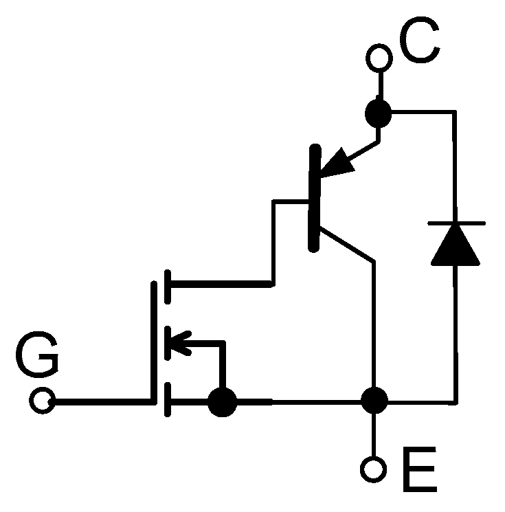
26] the IGBT is typically modelled using the network representation of this device shown in
Figure 1. As it is visible in the structure of the IGBT, three components can be distinguished: The MOSFET, the BJT and the diode.
On the basis of this classical IGBT structure presented in
Figure 1 a new dynamic model taking into account parasitic capacitances is elaborated. The network representation of the new model, based on the conception presented in
Figure 1, is shown in
Figure 2.
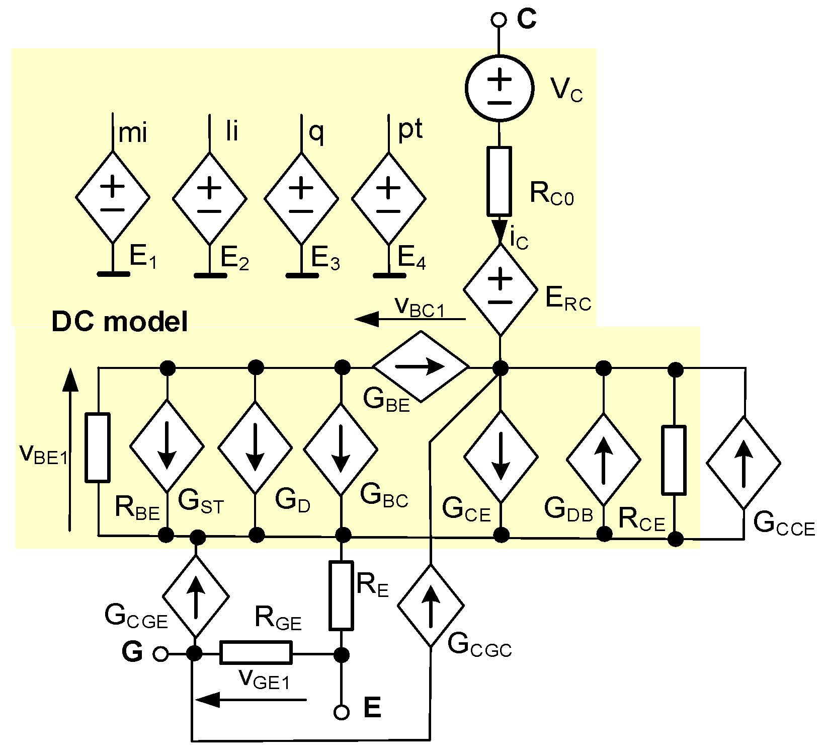
In
Figure 2, electronic components describing dc characteristics of the IGBT are marked with yellow colour and labelled as a dc model. In turn, controlled current sources G
CGE, G
CCE and G
CGC model currents flowing through internal capacitances
CGE,
CCE and
CGC, respectively, of the transistor. In analytical formulas describing the considered controlled current sources influence of temperature on the value of the mentioned capacitances is taken into account.
In the dc model of the IGBT, drain current of the internal MOS structure is represented by two controlled current sources: GD describing channel current of the MOS transistor and GST modelling the sub-threshold component of this current. To compute the values of currents and voltages in the model of the internal MOS structure, auxiliary controlled voltage sources (E1, E2, E3 and E4) are indispensable.
The controlled current source GBE represents current flowing between the base and the emitter of the bipolar transistor contained in the structure of the modelled transistor. In turn, the controlled current source GBC describes current flowing between the base and the collector of the bipolar transistor contained in the modelled IGBT.
The controlled current source G
CE models the main current of the IGBT. The controlled current source G
DB models dc characteristic of the diode. All the equations used to describe all the mentioned controlled current sources are described and discussed in paper [
16].
In order to model electric inertia of the IGBT controlled current sources G
CGE, G
CCE and G
CGC are used. The mentioned current sources model current flowing through parasitic capacitances of the transistor:
CGE,
CCE and
CGC, respectively. These currents are described with formulas presented below. Capacitance between the collector and the emitter is described by formula of the form analogous to formula describing p-n junction capacitance. Because this junction does not rapidly change into the forward mode, in the equation describing this capacitance the diffusive component is omitted, but influence of temperature on this capacitance is described by following formula:
where
VCE marks the collector emitter voltage,
CCE0—output capacitance of the IGBT at zero voltage on the diode,
Vj—built-in potential of reverse diode,
Mj—parameter describing the doping profile of the junction,
r—the temperature coefficient of parameter
Mj, Tj—internal temperature of the IGBT,
T0—reference temperature.
Capacitance between the gate and the emitter of the transistor is described by the following spline:
where
C0x is capacitance dependent on thickness of the layer of oxide under the gate
tOX,
w—width of the channel of the MOS structure,
CGE0—capacitance per unit of channel widths between the gate and the emitter,
VGEmax,
VGEmin,
CG1,
CG2,
x,
u and
k1—other parameters of the model, whereas
VGE and
VC1E are voltages marked in
Figure 2.
Capacitance
Cox occurring in Equation (2) is given by formula of the form [
8,
27]:
where
L denotes the length of the channel of the MOS structure,
is dielectric permeability of free air, and
relative dielectric permeability of silicon oxide.
Capacitance between the gate and the collector is described by the dependence of the form:
where
CGD0 is capacitance per the unit of channel width between the gate and the drain on the unit of the channel width,
C1,
C2,
y,
e,
n,
VGCmin—other parameters of the model,
Mj2—parameter describing the doping profile of this junction,
VjC—potential of the base-emitter junction,
q—electron charge
k—the Boltzmann constant,
iC—collector current.
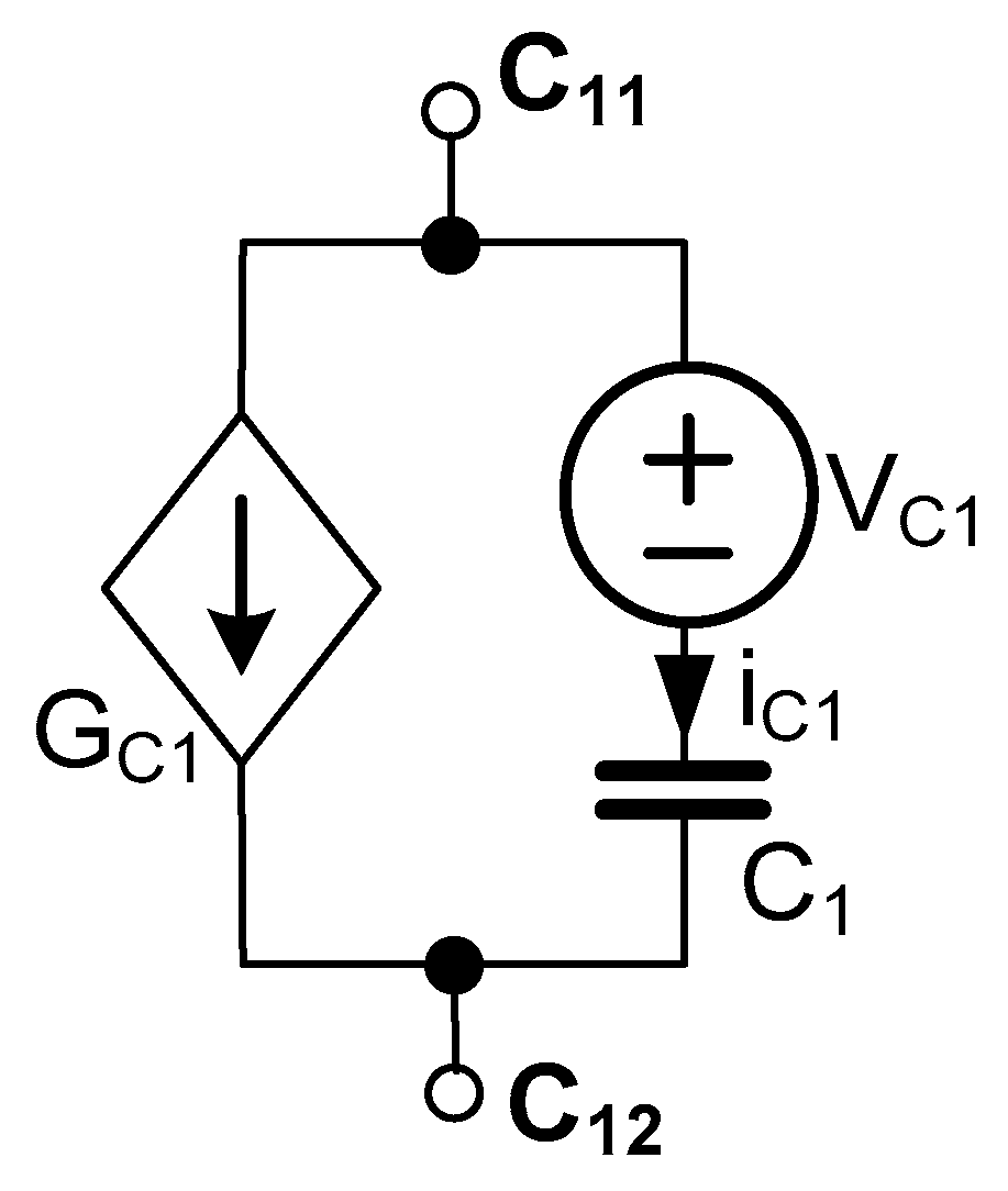
In practice, in order to model each of these capacitances, the use of a subcircuit shown in
Figure 3 is needed.
This subcircuit consists of linear capacitor C
1 of the fixed value of capacitance, voltage source V
C1 of the zero value and the controlled current source G
C1. The voltage source V
C1 is used to monitor the value of current i
C1, which is proportional to time derivatives of voltage on the current source G
C1 and on the capacitor C
1. The current flowing through the controlled current source G
C1 modelling parasitic capacitance
CX is given by the following formula:
In the presented dynamic model of the IGBT output currents of the considered controlled current source (GCCE, GCGE and GCGC) describing current flowing through parasitic capacitances of the IGBT are described by Equation (5), in which capacitance Cx is equal to the appropriate capacitances described with Equations (1)–(4).
3. Results of Computations and Measurements
In order to verify usefulness of the worked out dynamic IGBT model many computations and measurements of waveforms of collector current while switching-on and switching-off this device were performed. Measurements were realised in the measurement set-up shown in
Figure 4.
In the presented measurement set-up, voltage source VCC feeds the collector of the investigated device. The control signal is generated by the function generator and is amplified by the driver MCP1305. Resistor RL limits collector current and resistor RG limits the maximum current of the gate of the tested IGBT. In the measurement set-up the oscilloscope Rigol DS1052E, the current probe Tektronix TCPA 300, the feeder NDN of the type DF1760SL10A and the functional generator of the type NDN JC5603P are used. The case temperature of the investigated device is measured by the pyrometer Optex PT-3S. The band of the applied oscilloscope is 50 MHz, and the current probe −100 MHz. The applied driver is characterised with the maximum output current of 4.5 A and with the maximum output voltage amounting to 18 V. During measurements the investigated transistor is situated in the thermostat.
Investigations were performed for type the IRG4PC40UD transistor [
28] manufactured by International Rectifier company. During measurements this transistor was screwed to a large aluminium heat-sink situated in the thermostat. The gate of this transistor was controlled by a rectangular pulses train. The amplitude of this signal was equal to 15 V, whereas its frequency was equal to 20 kHz. Resistor R
G of resistance equal to 210 Ω was connected in series with the gate of the transistor. In order to minimise influence of a self-heating phenomenon on the investigated waveforms, all the measurements presented in this section were obtained just after switching-on or switching-off the control signal.
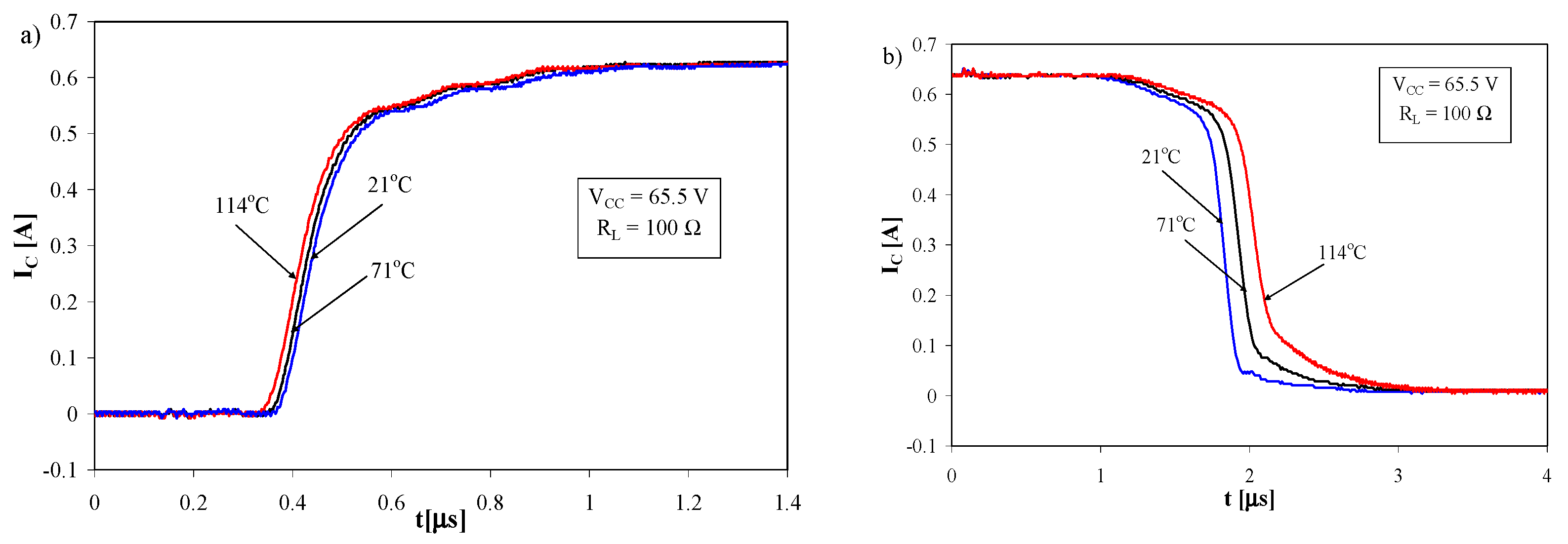
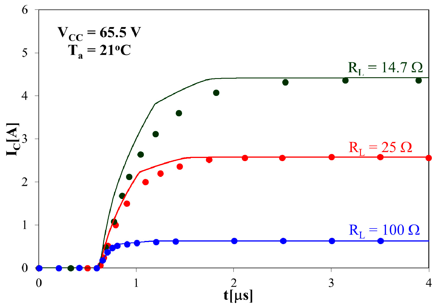
In
Figure 5 influence of temperature on the measured waveforms of collector current obtained at selected temperature values in the range from 21 to 114 °C is shown. Such a range of investigations was selected arbitrarily taking into account three reasons. Firstly, the lowest value of temperature should be equal to typical room temperature. Secondly, the highest value of temperature must be lower than the maximum allowable temperature of operation of the considered transistor. Thirdly, differences between the highest and lowest temperature should be possibly big to visibly illustrate influence of temperature on dynamic properties of the tested transistor.
During measurements, the collector circuit of the tested IGBT was fed from the source VCC of constant voltage equal to 65.5 V Resistor RL of resistance 100 Ω which was connected between this source and the collector of the tested transistor. As it is visible, temperature very weakly influences waveforms IC(t) while switching-on, whereas influenced of temperature on these waveforms was strong while switching off. In particular, considerable extension of the so-called current tail could be observed at a temperature rise. The temperature rise caused acceleration of the switching-on process of the investigated transistor by 50 ns and a slowdown of the switching-off process of this transistor by almost 500 ns.
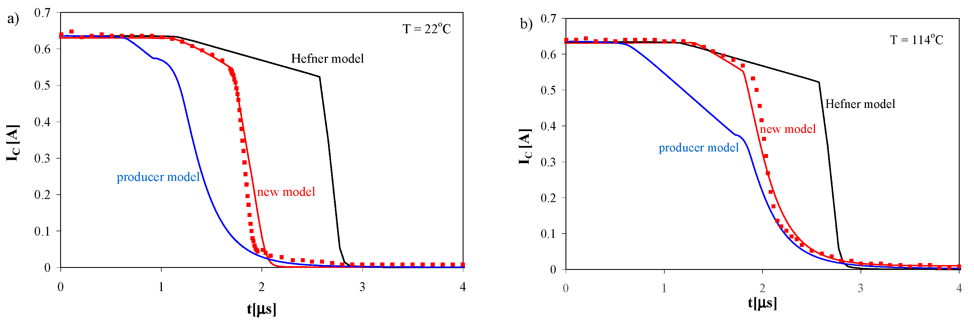
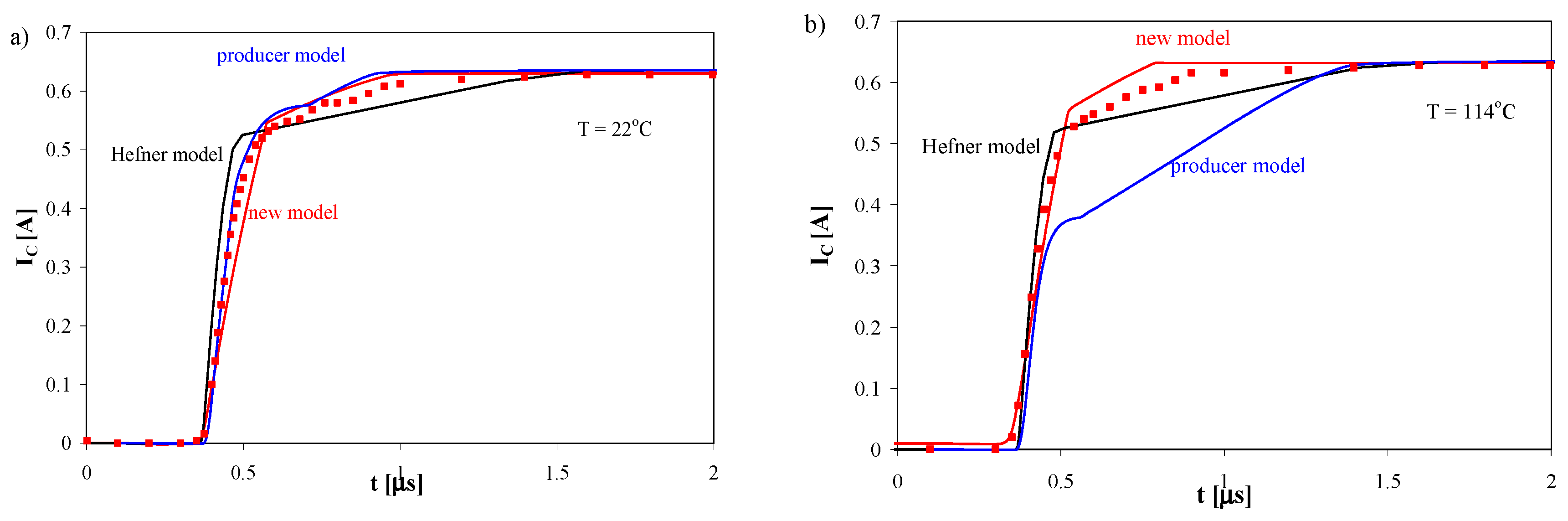
Using the presented in the previous section dynamic model of the IGBT, waveforms of voltages and currents of the considered device during the switching process at fixed values of temperature were computed. The results of computations obtained using the authors’ new model are presented in
Figure 6,
Figure 7 and
Figure 8 as red lines. They are compared with the results of measurements (points) and the results of computations obtained by means of two popular literature models—the Hefner model [
27,
29] built-in in the SPICE (black lines) and the model available at the website of International Rectifier [
15] (blue lines).
The considered literature models were described in detail in paper [
16].
Figure 6 shows waveforms of collector current during the switching-off process of the considered device supplied in the identical manner as in the case considered in
Figure 5. The results shown in
Figure 6a correspond to temperature equal to 22 °C, whereas the results shown in
Figure 6b correspond to temperature equal to 114 °C.
As it is visible, good agreement was obtained between the results of computations and measurements at both the considered values of temperatures only for the authors’ model. For the producer model [
15], the switching-off process ran too quickly, especially for temperature T = 22 °C. In temperature equal to 114 °C, essential improvement in accuracy of computations performed with the described model within the range of current values below 300 mA could be observed. In turn, the results of computations obtained with the use of the Hefner model were characterised by the overlong switching-off process. Similarly, as it was presented for dc characteristics in paper [
16], this model does not take into account influence of temperature on the shape of characteristics of the considered device.
Figure 7 shows waveforms of collector current of the investigated IGBT during the switching-on process for temperature equal to 22 °C (
Figure 7a) and 114 °C (
Figure 7b).
At temperature equal to 22 °C good agreement between the results of measurements and computations was obtained for all the tested models. In contrast, for temperature T = 114 °C good agreement between the results of computations and measurements was obtained with the use of the authors’ model, and acceptable agreement between these results was assured also by the literature models. The producer model is characterised by good accuracy only within for values of collector current below 300 mA.
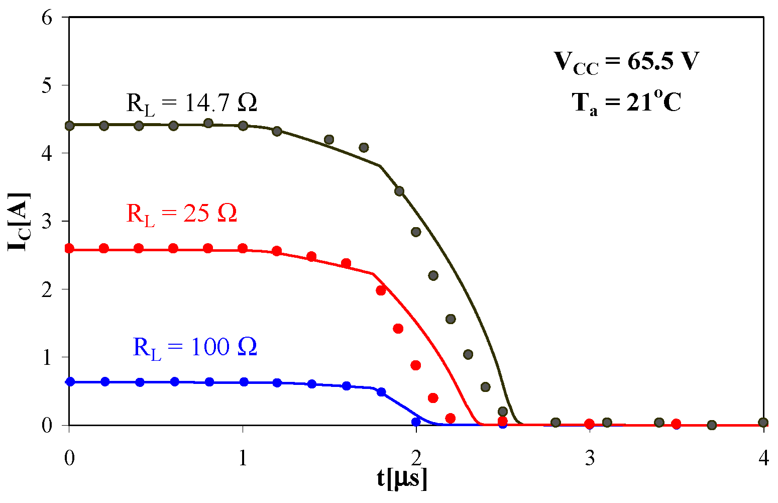
Figure 8 illustrates waveforms of collector current during the switching-on process (
Figure 8a) and the switching-off process (
Figure 8b) of the tested IGBT operating at room temperature and load resistance R
L equal to 14.7 Ω.
Only for a new model good agreement between the results of measurements and computations was obtained. Computations performed with the use of both the literature models showed incorrectly too short duration time of the switching-on process. In turn, the computed with the use of these models waveform of collector current during the switching-off process showed too short duration time of this process for the producer model and too long—for the Hefner model.
Comparing the results of measurements and computations obtained for different values of load resistance (
Figure 6a,
Figure 7a and
Figure 8), it is visible that at a higher value of this resistance both the considered switching times are shorter than for a lower value of resistance R
L.
Table 1 shows the values of times t
on and t
off computed with the use of three considered models and measured values which correspond to different values of resistance R
L and temperature. As one can notice, in five out of six considered cases the value of the mentioned times was computed with the use of the author′s model. In the case of time t
off computed at temperature 114 °C and resistance R
L = 100 Ω the value of this time was obtained with the use of the producer model. However, as it is visible in
Figure 6b, this model does not describe exactly the whole course of collector current during the switching-off process, so the accurately computed value of time t
off results from good modelling of the coordinates of only two points in the waveform I
C(t) used in computing values of parameters shown in this table.
As it visible in the presented comparison of the results of computations and measurements (
Table 1), only the authors’ model assured good accuracy. The computed by means of both literature models waveforms of collector current while switching significantly differ from the results of measurements. The proposed model is correct over a wide range of changes of temperature and load resistance.
As it can be observed, the literature models assured good agreement between the results of computations and measurements only in the case of the process of switching-on at room temperature. In other operating conditions visible differences between the results of computations and measurements were observed. In turn, the authors’ model correctly described influence of temperature on waveforms of collector current both while switching-on and switching-off the transistor.
Using the authors’ model, waveforms of the collector current while switching-off (
Figure 9) and switching-on (
Figure 10) the considered transistor are computed and the obtained results of computations are compared to the results of measurements.
In
Figure 9 it is visible that the time of switching-off increases together with an increase of the switched current. In the investigated range of current i
C values, time of switching-off increases from 1.22 μs to 2.34 μs. This increase is linear and time of switching-off increases with an increase of current with the slope equal to about 94 ns/A.
In
Figure 10 it is visible that the on-time increases together with an increase of the switched current. In the investigated range of values of currents i
C, the on-time increases from 620 ns to 1.69 μs. This increase is linear, and the on-time increases with an increase of current of 186 ns/A. This increase is double compared to the case of switching-off.
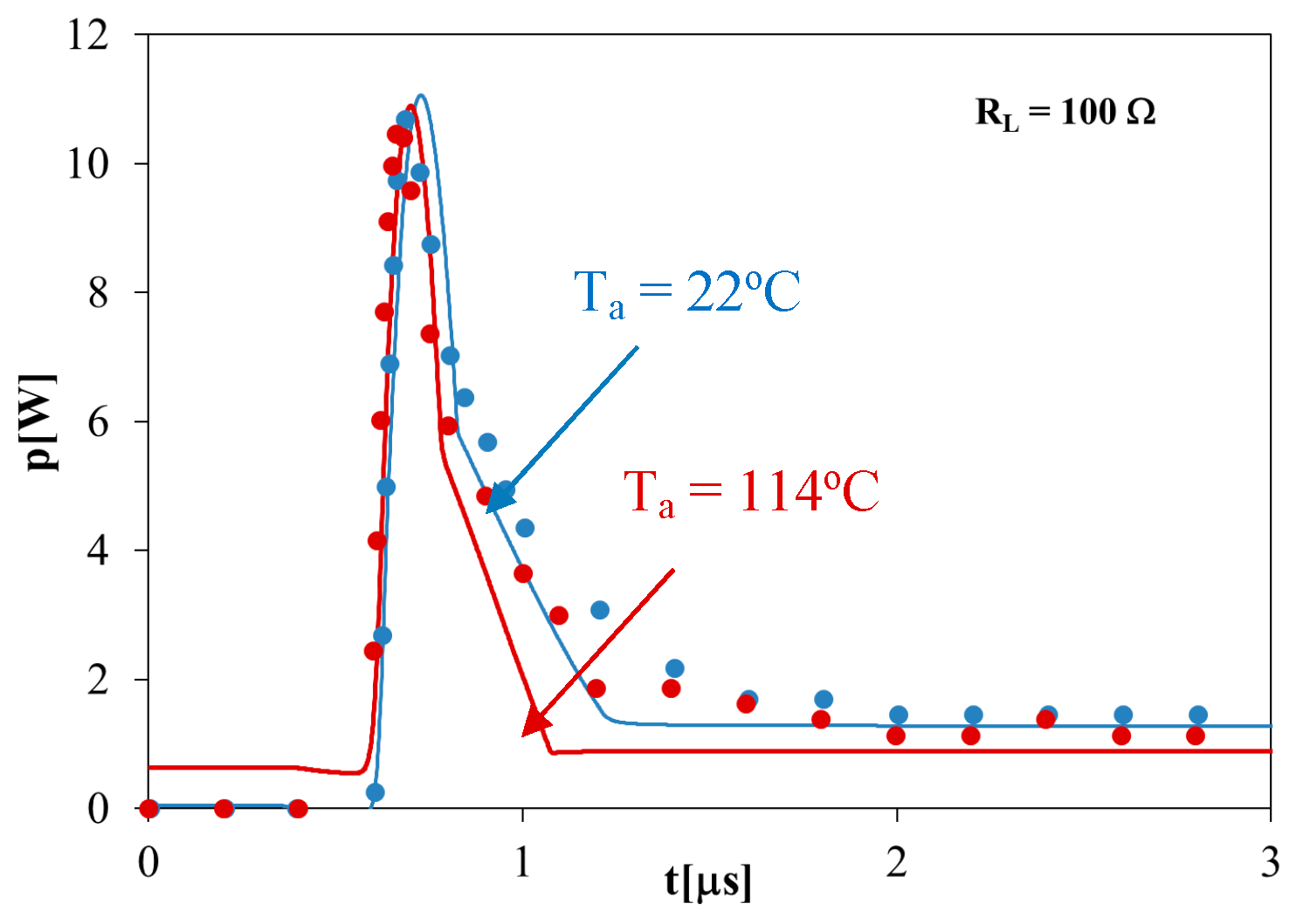
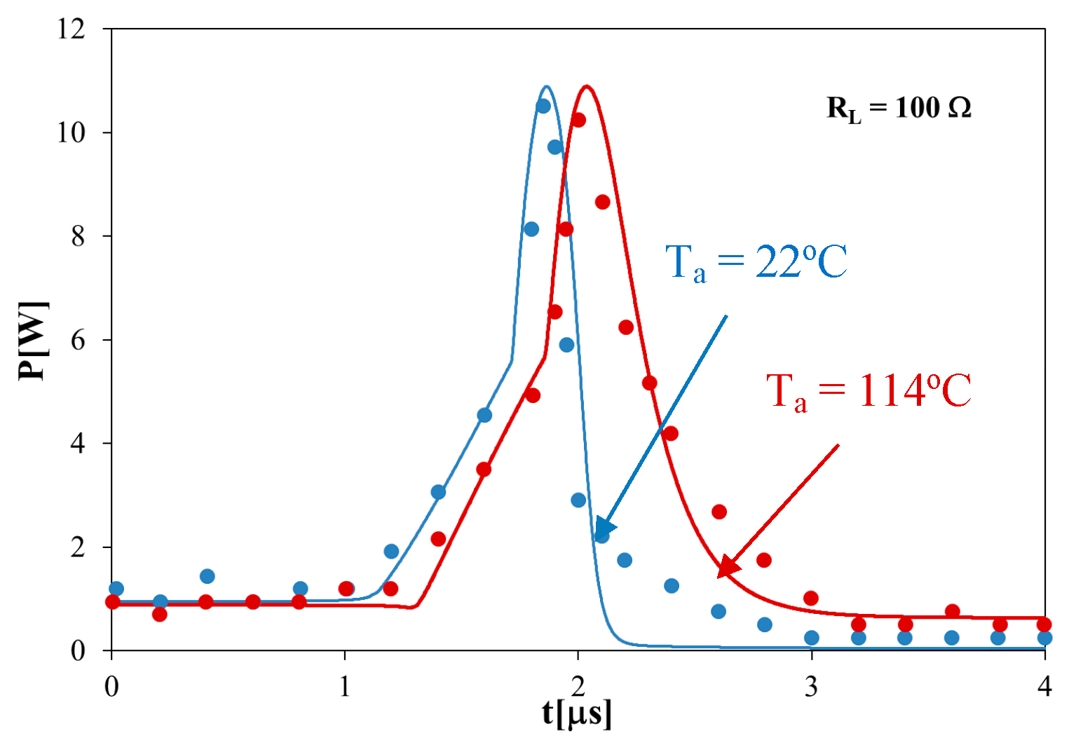
From the point of view of switched-mode electronic circuits energy losses during the switching process are essential. In
Figure 11 and
Figure 12 the computed and measured waveforms of power losses in the investigated transistor at two different values of temperature are presented.
Figure 11 shows a shift between the maxima of courses p(t) obtained while switching-off in the considered temperatures, whereas the corresponding waveforms p(t) while switching-on shown in
Figure 12 differs between one another imperceptibly.
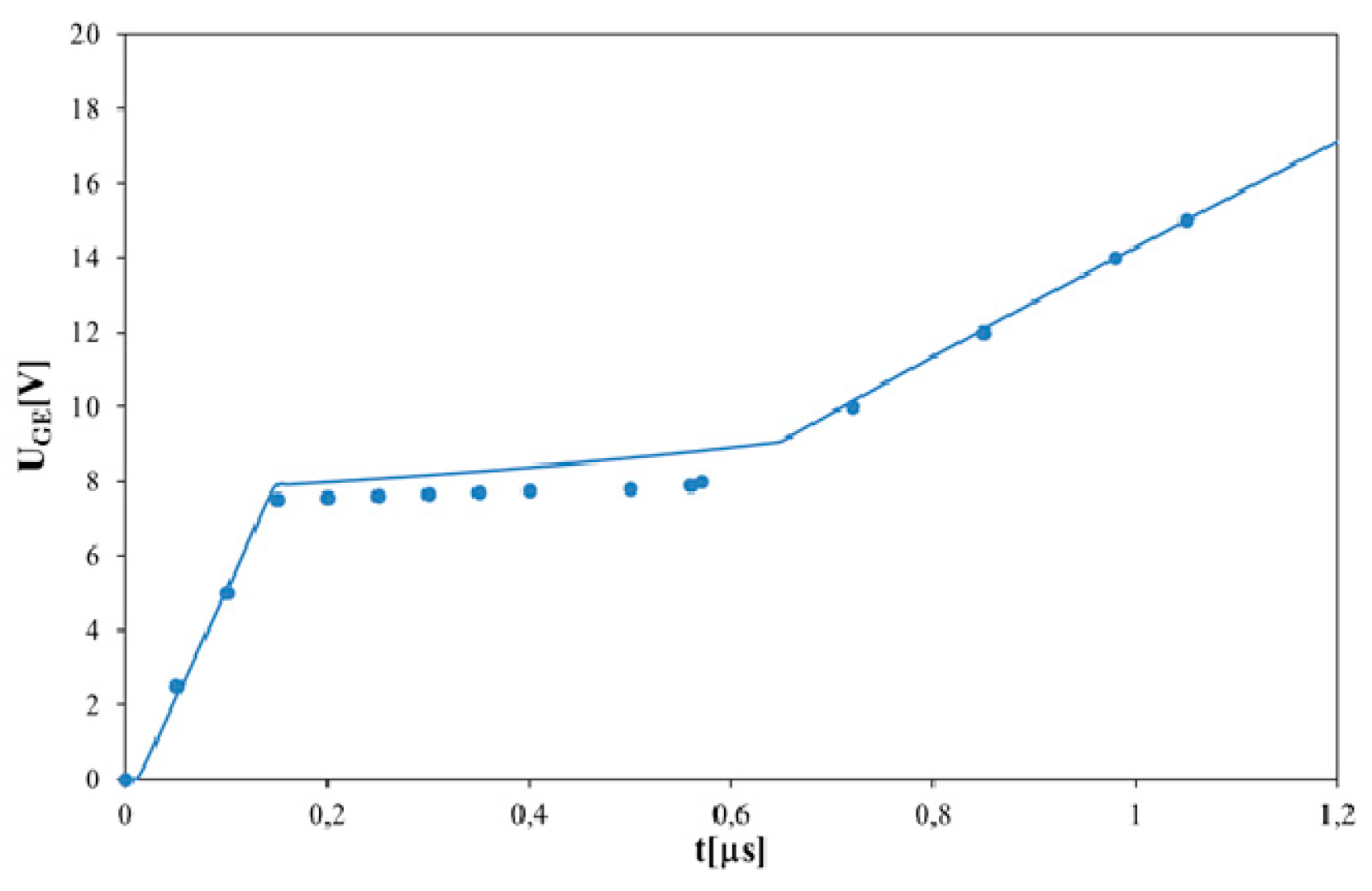
In
Figure 13 the computed and measured waveforms of gate-emitter voltage while charging the gate of the investigated transistor are presented. These waveforms were measured and computed for collector current I
C = 20 A and voltage feeding the collector V
CC = 400 V. Current of the gate during the test amounted to 100 mA. As it is visible, the results of computations and measurements are convergent and satisfactory; the differences between them do not exceed 10%. This confirms correctness of the description of input capacitance of the considered transistor.
4. Conclusions
In this article a new form of the IGBT model dedicated for the SPICE software is proposed. This model takes into account influence of temperature on dynamic properties of the considered device. In the description of the proposed model new dependences of device parasitic capacitances on temperature and on the co-ordinates of the device operating point are included in the form of analytical formulas.
The usefulness of the elaborated model is verified for the transistor operating as a switch. Waveforms of collector current are computed with the use of the new model and two models given in the literature. Computations are performed at different values of temperature and load resistance. The results of computations are compared to the results of measurements. The waveforms of collector current while switching-on and switching-off obtained using the new model fit well the results of measurements in the whole considered range of changes of temperature and load resistance. In contrast, the results of computations obtained using the considered literature models visibly differ from results of measurements. The difference increase while load resistance decreases.
The performed computations and measurements prove correctness of the new model. It is also visible that temperature strongly influences the value of off-time, but its influence on on-time could be omitted. Moreover, it is also shown that the new model properly describes waveform of power dissipated in the investigated transistor while it is being switched. Correctness of the used description of the transistor input capacitance prove good agreement between the computed and measured waveforms of gate-emitter voltage while charging the gate.
The disadvantage of the proposed model is a complicated description of internal capacitances making use of splines. It could result in some problems with convergence of the analysis performed for a long time—equal to hundreds or thousands of periods of the signal controlling the gate of the considered transistor.
The presented dynamic model of the IGBT could be useful for designers of power electronics circuits, making possible realisation of more accurate computer simulation of such circuits. This model could be also useful in didactics to present influence of temperature changes on switching-on and switching-off processes in power converters including IGBTs.
As it is commonly known, temperature of the IGBT could change as a result of self-heating phenomena [
17]. Therefore, in further investigations the authors will elaborate an electrothermal model of the IGBT on the basis of the dynamic model presented in this article.


