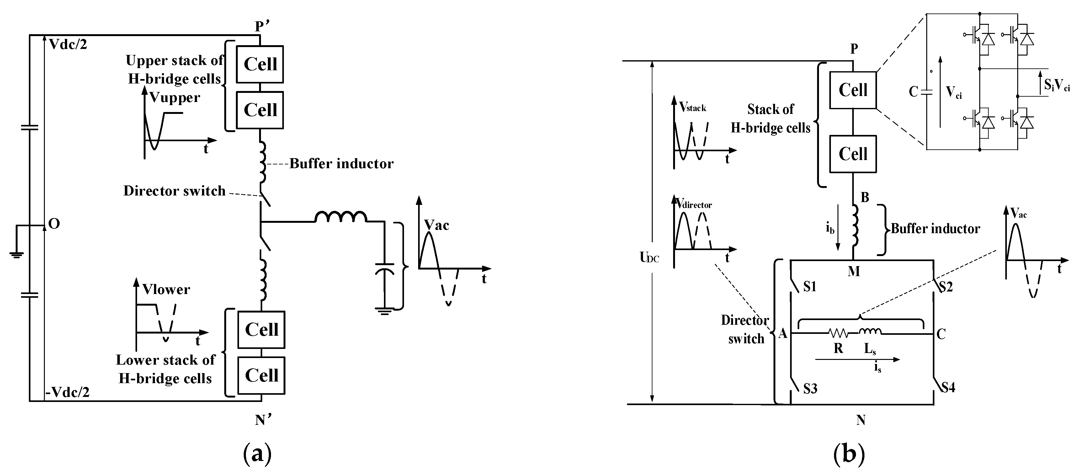
Article

A Full-bridge Director Switches based Multilevel Converter with DC Fault Blocking Capability and Its Predictive Control Strategy

Institute of Electrical Engineering, Chinese Academy of Sciences, Haidian District, Beijing 100190, China
*
Author to whom correspondence should be addressed.
Energies 2019, 12(1), 91; https://doi.org/10.3390/en12010091
Submission received: 23 October 2018 / Revised: 19 December 2018 / Accepted: 21 December 2018 / Published: 28 December 2018

Abstract

:
Voltage source converter-based high-voltage direct current transmission system (VSC-HVDC) technology has been widely used. However, traditional half-bridge sub module (HBSM)-based module multilevel converter (MMC) cannot block a DC fault current. This paper proposes that a full-bridge director switches based multi-level converter can offer features such as DC side fault blocking capability and is more compact and lower cost than other existing MMC topologies. A suitable predictive control strategy is proposed to minimize the error of the output AC current and the capacitor voltage of the sub-module while the director switches are operated in low-frequency mode. The validity of the proposed topology and control method is demonstrated based on simulation and experimental studies.

1. Introduction

The modular multilevel converter (MMC) has been accepted as a suitable solution for high-voltage and high-power application fields due to several inherent features [1,2,3,4,5,6,7,8]. However, blocking the DC fault current becomes a difficult problem because the anti-parallel diodes are still conducting after the insulated-gate bipolar transistors (IGBTs) of HBSM are turned off [9].
To solve this problem, recent research has highlighted a number of interesting converter topologies which combine the features of the multilevel output AC voltage waveform and DC fault blocking capacity [9,10,11,12,13,14,15,16,17,18,19,20,21,22]. Full-bridge sub-module (FBSM) based MMC (F-MMC) is a basic configuration with DC fault current blocking capacity [10,11]. However, the DC fault current blocking capability comes at a cost of nearly doubling power losses and number of semiconductor devices. Some other type of sub-module is proposed instead of FBSM to make a further optimization in reducing the number of IGBTs, such as a clamp double sub-module (CDSM) proposed in [14,15] and a three-level cross-connected sub-module (TCSM) proposed in [16]. Several hybrid MMC topologies are also proposed, based on HBSM and those various types of sub-module [9,12,13,16,17,18,19,23], for further reducing the cost and loss on the premise of having the DC fault blocking capacity, such as hybrid MMC based on CDSM and HBSM (CH-MMC). However, there are still some drawbacks, for example, as they are composed of a large number of sub-modules, the system needs to be more complicated and the converter station bulkier.
The alternate-arm multilevel converter (AAMC) based on the hybrid topology of HBSM and director switches is proposed in [20,21,22]. The AAMC further improves the traditional MMC topology by cutting the number of sub-modules, reducing DC bus voltage, and gaining the ability to block DC fault currents [22]. However, some features still have the possibility for further optimization, such as the size and cost of the overall system. One of the main technical challenges associated with the control of such a director switches based multilevel converter is to simultaneously keep the capacitor voltages balanced and provide good output current tracking performance, while the director switches keep switching in low frequency.
In order to further optimize the size and cost of the voltage source converter-based high-voltage direct current transmission system (VSC-HVDC) converter with the blocking ability of DC faults, this paper proposes a full bridge director switches based alternate-arm multi-level converter (FA-MMC) and a corresponding control strategy:
  • The size and cost of the overall system can be significantly reduced by reducing the number of SM capacitors, IGBTs, and other related devices. In addition, an FA-MMC retains the ability to block DC-side faults since it uses H-bridge SMs as the AAMC.
  • Similar to AAMC, a systematic multi-objective control method is needed for this kind of topology to minimize the error of output AC current and the capacitor voltage of the sub-module while the director switches are operated in low-frequency mode. A suitable predictive control strategy for this kind of topology is presented in this paper to achieve the flexibility to include the previously mentioned multiple system requirements.

2. Proposed Topology

2.1. Structure and Basic Operation

The basic circuit configuration of full-bridge director switches based modular multi-Level converter (FA-MMC) proposed in this paper is shown in Figure 1b. The proposed topology consists of a stack of H-bridge SMs and four director switches (S1–S4) made of series IGBTs or IGCTs. The ability of DC-side fault blocking is still retained since the H-bridge SMs structure is the same as the AAMC.
The voltage of the director switches (Udirector in Figure 1b) is equal to the DC voltage (UDC in Figure 2) plus the voltage produced by the stack of H-bridge SMs which can be considered as only one controllable voltage source. Therefore, the voltage of director switches can be adjusted flexibly so that the switching of S1–S4 can switch at near to zero voltage. The ideal voltage waveform is shown in Figure 2a.
The working cycle of S1–S4 is synchronized with the output AC voltage. S1 and S4 are conducting and S2 and S3 are turned off while the output AC voltage (Uac in Figure 1b is in its positive half-cycle, in contrast, S2 and S3 are conducting and S1 and S4 are turned off while the output AC voltage is in its negative half-cycle. This ensures that the four director switches can switch at low-frequency and at the point of zero-voltage-crossing as shown in Figure 2a. These features lead to low switching losses, and low demand for dynamic voltage sharing at the switching instant of the series switches, so that the system design has been simplified.

2.2. Energy Balance

When the AC current flows through the stack of H-bridge sub module. In order to ensure the continuous operation of the system, the energy balance of the stack of H-bridges should be guaranteed. The amount of energy transferred from the AC side (EAC) and going to the DC side (EDC) should be equal over half the fundamental period and is given as
E A C = 3 2 V A C I A C ω π cos ( φ ) ,
E D C = 6 U D C I A C ω cos ( φ ) ,
For EAC to equal EDC, the relationship between the DC voltage magnitudes and AC voltage magnitudes mentioned in Equations (1) and (2) can be given as
U D C = π 4 V A C ,
However, since the converters can’t operate in the perfect given by Equation (3), an energy balancing strategy should be used.
Reference [22] presented two methods to achieve energy balance for AAMCs that can also be used in this topology: Overlap current and third harmonic current injection. In this paper the overlap current method is used to extend the period when the current directed from S1 and S4 to S2 and S3 is extended and S1–S4 are all conducting. The overlap current is used to exchange power between the sub module capacitors and the DC bus. The load current is only slightly affected, since the overlap time is very short and the inductance can smooth the change in current. Considering its effect on the grid current, the overlap time is determined to be less than 0.8 ms.

3. Predictive Control Strategy

The control strategy of the proposed topology requires minimizing the error of the output current and DC voltage in each sub module, and, meanwhile, the director switches switching should be operated in low-frequency and zero-voltage switching mode.

3.1. Dynamic Modeling

Based on Figure 2, the governing equations of the single-phase FA-MMC can be shown as follows:
U D C V P B L b d i b d t = V M N
V A C = L s d i s d t + R i s
V A C = S d V M N
As presented in Section 2, the value of Lb is small and the voltage on it can be ignored; S1–S4 have five switching state combinations depending on a switching function Sd as shown in Table 1.
The output voltage of each H-bridge sub module is equal to Vci (capacitor voltage of the ith sub module (i = 1, 2, ⋯, n)), −Vci, or zero, depending on the switching states, and depends on a switching function Si
S i = { 1 0 1   ( i = 1 ,   2 ,   ,   n ) .
The relationship between Vci and UDC is formalized as
i = 1 n V c i U D C
Based on Equation (16) and the basic principle, VPB is formalized as
i = 1 n S i V c i = V P B
The dynamic capacitor voltage of the cells of the H-bridge sub module in Figure 1b is formalized as
S i i b = C d V c i d t
The relationship of currents is and ib in Figure 1b, which was also indicated by the switching function Sd according to Table 1, is expressed as
i b = S d i s   ( S d = 1   or   1 )
L d i b d t = U D C i = 1 n S i V c i   ( S d = 0 )
The switching states of director switches operate in an energy balancing mode, as mentioned in Table 1. As discussed previously, the current ib flows through the stack of H-bridge sub modules, buffer inductor, and director switch to the DC side, charging or discharging the capacitor of the H-bridge sub modules.
Only considering the basic operating mode, substituting Equations (5), (6), (9), and (11a) into (4), a dynamic model of the single-phase proposed topology in basic operating mode can be expressed as
S d ( U D C i = 0 n S i V c i S d L b d i s d t ) = L s d i s d t + R i s
where Sd = 1 or −1. Equation (12) can be simplified as
L d i s d t = S d ( U D C i = 0 n S i V c i ) R i s
where L = Lb + Ls.

3.2. Proposed Predictive Control

The predictive control strategy is proposed in this section based on the dynamic model of the FA-MMC presented above, the three primary targets of the predictive control strategy is achieved as follows:

3.2.1. AC-Side Current Control

Assuming a sampling period of Ts, a discrete-time model of the FA-MMC AC-side current in basic operating mode based on Equation (3) is calculated by
L T s ( i s ( k + 1 ) i s ( k ) ) = S d ( k ) ( U D C ( k ) i = 0 n S i ( k ) V c i ( k ) ) R i s ( k )
the value of Sd could be assumed as a constant value during a short sampling period of Ts. is(k) is the actual AC current at time k and is(k + 1) is the predicted AC current at time k + 1, UDC(k) can be considered as a constant value if the DC side voltage is controlled. Finally, Vci(k) is the capacitor voltage of the sub module i at time k.
To reduce the error between the predicted current and the reference current, a cost function associated with the current error is defined as
J i = | i s r e f ( k + 1 ) i s ( k + 1 ) |
where isref is the reference current and is(k + 1) is the predicted current obtained from Equation (14). Ideally, Ji will be equal to its minimum value of (Jmin = 0 in Figure 3) if the AC-side current is controlled well.

3.2.2. Capacitor Voltage Balancing

Based on Equations (10) and (11), Vci (k + 1) can be deduced as
V c i ( k + 1 ) = V c i ( k ) + S i ( k ) S d ( k ) i s ( k ) C T s
where Vci(k) can be measured in real time. Another cost function for balancing the capacitor voltage of sub modules is given as
J v c = i = 1 n | V c i ( k + 1 ) V c i r e f ( k + 1 ) |
where Vciref(k + 1) is the reference DC capacitor voltage of sub module i (with i between 1 and n), which can be equal to the average voltage of all cells (given as i = 1 n V c i ( k + 1 ) n ), and Vci(k + 1) is a predicted value, which can be obtained from Equation (16).
Consequently, by adding the above cost function together a combined cost function, which can simultaneously achieve the two main control objectives mentioned above is given as the linear combination
J a l l = α J i + β J v c
where α and β are weighing factors, α is adjusted based on the cost contribution allocated to the error of AC-Side current, and β is adjusted based on the cost contribution allocated to the voltage deviations of sub module capacitors. The empirical method to determine the value of cost function is presented in [24].
Within each sampling and computing period Ts, the combined cost function Jall is re-calculated, and the best switching indicated to the minimum value for Equation (18) will be adopted for the current control cycle.

3.2.3. Director Switch Control

As presented in Figure 2a in Section 2.1, the state of director switches S1–S4 at the next step should depend on the value of VAC. According to Equation (5), the necessary value of VAC at the current step can be expressed as
V A C ( k + 1 ) = R i s r e f ( k + 1 ) + L s T s ( i s r e f ( k + 1 ) i s ( k ) )
However, the fluctuation of VAC(k + 1) due to differences between isref(k + 1) and is(k) during zero voltage crossings will lead to high frequency repeated switching of S1–S4, resulting in an increase of switching losses.
Therefore, a director switch control strategy should be taken considering the need to
  • Add the energy-balancing mode (Sd = 0 in Table 1) in to achieve energy balancing of the stack of H-bridge by exchanging power with DC bus.
  • Avoid repeated switching of the director switches.
Replacing is(k) by isref(k), the necessary value of VAC at the current step can be expressed as
V A C r e f ( k + 1 ) = R i s r e f ( k + ` 1 ) + L T s ( i s r e f ( k + 1 ) i s r e f ( k ) )
where isref(k) is the reference value of the current of the current step. Voltage VACref(k + 1), obtained by Equation (20), is a standard sine wave, which can avoid the fluctuation of VAC(k + 1) due to differences between isref(k + 1) and is(k) during zero voltage crossings. Finally, the implementation procedure of the proposed director switch control strategy is summarized in Part I of Figure 3. The schematic diagram of the control system is shown in Figure 4.

4. Simulation Results

This section evaluates the performance of the proposed FA-MMC and control method with a simulation. The simulation parameters are given in Table 2.

4.1. Operating Performance under a Steady-State Condition

Figure 5 shows the voltage of the stack of H-bridges cells, the voltage across the director switches S1–S4, and the AC output voltage while the load current tracks the reference in steady-state operation. The simulation results are consistent with the working principle of the topology described in Figure 1b of Section 2. The voltage waveforms appear staircased because there are only two cells, while they would more closely resemble a sine curve with an increase in the number of cells. Figure 6 shows that the capacitor voltages in the two cells are averaged well and mostly under the control of MPC in basic operating mode. Further, they get closer to the given value UDC/ncell_FA in energy-balancing mode.
Figure 7 shows the director switch control signal of S1–S4. It can be seen in Figure 7a that they all operated at a frequency of 100 Hz and achieved zero voltage switching under the director switch control strategy described in Part I of Figure 3. In contrast, when Part I of Figure 3 is removed, the director switch control signal, which is only determined by VAC(k + 1), is shown in Figure 6b. The difference in responses occurs because VACref(k + 1) in Equation (20) is obviously a standard sine wave while the VAC(k + 1) is repeatedly crossing the zero voltage point as shown in Figure 8. This demonstrates the effectiveness of the director switch control strategy.
Figure 9 reveals that the relation of the current across Lb (Ib in Figure 9) and the load current (Is in Figure 9) is similar to Equation (11a) in basic operating mode. The current across Lb (Ib in Figure 9) becomes an overlap current that charges or discharges the capacitor of the cells when S1–S4 are all conducting in energy balancing mode.

4.2. Operating Performance under a Transient-State Condition

To test the dynamic performance, a sudden change in the reference current is set at 0.04 s, and the behavior of the system is shown in Figure 10. It can be seen that the current tracked the reference value well. The time of reference tracking (from 600 A to −600 A) is less than 0.01 ms as shown in Figure 10b, and the output AC voltage waveform is shown in Figure 11.
The capacitor voltage is shown in Figure 12. It can be seen that the capacitor voltage of the two sub-module remains balanced after a sudden change of load current. Figure 12b shows that there is a deviation in the beginning, but is averaged well immediately by the predictive control strategy after 1 ms.
Figure 13 shows the states of the director switches at the instant of the sudden change of load current, demonstrating that the director switches are controlled well and operated in low-frequency mode.

4.3. Operating Performance under a DC Fault

Having verified the normal operation of the converter, the model was tested under a DC fault. A three-phase model was built, and a DC fault was induced at 0.04 s. The blocking time is set to be 3 ms after the fault current is detected considering the sensor delay time. Figure 14 shows that the voltage of the cell capacitor is kept at 1.5 kV and the AC current follows the given value before 0.04 s. When a DC short-circuit happens at 0.04 s, the direction of current is reversed and the AC side current rises at first because during the sensor delay, the capacitors discharge and current flows from the AC side to the DC side. After 3 ms, when the converter station is blocked, the DC and AC side currents gradually reduce to zero along with the charging of the capacitor.

5. Experimental Results

Experiments on an FA-MMC-based inverter were also carried out to verify the proposed topology and test the predictive control strategy. The parameters for the experiment are listed in Table 3. A photo of the inverter is shown in Figure 15 and an IGBT is utilized as the power switch. The main control algorithms were implemented in a combination of a DSP and FPGA. The DC-link voltage was obtained via a three-phase autotransformer.
To test the system balance ability, a 100 Ω resistor was shunted to capacitor SM2. The topology worked in this unbalanced condition by appropriately setting the value of the weighting factor β, which is used to balance the capacitor voltage of the two SMs to zero. In this paper, we set the weighting factor α to a fixed value of 50, and set weighting factor β to 0 or 100 to compare the waveforms. Figure 16 shows the capacitor voltages of the two SMs. At first, the capacitor voltage of SM1 is lower than SM2, and the fluctuation is larger due to the unbalanced condition. After giving a suitable value to weighting factor β, each cell capacitor voltage is well regulated to their reference value and the fluctuation of the two cells is also the same.
Figure 17 and Figure 18 show the output current and voltage of this topology, which are both measured during balanced and unbalanced operation. From Figure 18 we can see that the voltage ripple of the two cell capacitors does not affect the current, apparently due to the robustness of the predictive control. When the weighting factor β is set to 100, meaning that the capacitor voltage balance is considered as a control goal, only a slight distortion is introduced into the output current.
To test the dynamic performance, the behavior of the FA-MMC and corresponding control method for a step in the angle of the reference current is shown in Figure 19. The waveforms show that the voltage changed quickly to drive the current to its new reference value and that the current is well-tracked. Figure 19 also shows that the dynamic capacitor voltage waveform is not influenced by the step in the angle of the reference current. Figure 20 shows a detailed view of the output voltage and current for a step in the angle of the reference current. The reference tracking of the proposed method that considered the possible switching states adjacent to VAC(k + 1) is fast, because extreme voltage changes are possible. The results are similar to simulation results.

6. Characteristic Analysis and Comparison with Other Topologies

6.1. DC Fault Blocking Capacity

When a DC-side short-circuit happens, with all IGBTs turned off, the director switches and stack of H-bridges behave as a number of uncontrolled diodes connecting with all DC capacitors in the cells connected in series, as shown in Figure 21. The equivalent capacitor value in Figure 21 can be expressed as
C e = C / n c e l l _ F A
where C is the capacitance of the capacitor in each cell and ncell_FA is the number of cells in one phase of the FA-MMC. The AC source charges the equivalent capacitor and inductors (including the Ls, Lb, Ld) through the DC fault current, thus, limiting the rising rate of the fault current. Consequently, the value of Uce will rise rapidly, and the DC fault current will be blocked.

6.2. Number of Sub-module and IGBTs

Equation (3) shows that the DC bus voltage is lower than the peak value of output AC voltage by 27% in FA-MMC topology. This implies that the voltage rating of the director switches should be at least equal to the peak value of output AC voltage since they have to support higher voltages.
Assuming that the maximum allowable working voltage rating of the IGBTs is equal to the voltage rating of the DC capacitors in the sub-modules, the number of sub-modules of the proposed FA-MMC is given by
n c e l l _ F A = U A C U R A T E D
where URATED is the voltage rating of the IGBTs. The number of IGBTs of each phase of the FA-MMC is given by
n I G B T 1 = 4 n c e l l _ F A + 4 n S = 8 U A C U R A T E D
where nS, the number of IGBT in S1–S4, is given by
n S = V M N U R A T E D = U A C U R A T E D
Given the same AC output voltage, we also can deduce the DC voltage, number of cells, and IGBTs needed in an AAMC. The relationship between DC and AC voltage magnitudes in an AAMC, which has been derived in [22], can be expressed as
V d c = π 2 V A C
It can be seen from Equation (3) and (25) that the FA-MMC can reduce the DC bus voltage by half with the same AC output voltage and same active/reactive power flow compared with an AAMC.
Considering the sum of the sub-module capacitor voltage must be greater than the peak value of the line-to-line voltage to achieve DC current blocking capability, the number of sub-modules of an AAMC can be expressed as
n c e l l _ A A = 3 U Λ A C U R A T E D
But, it only has two direct switches, so considering Equation (24) and (26), the number of IGBTs of a single-phase AAMC is given by
n I G B T 2 = 4 n c e l l _ A A + 2 n S = ( 4 3 + 2 ) U A C U R A T E D
To summarize, the number of IGBTs of the FA-MMC is less than that of the AAMC, and the DC voltage and number of sub-modules of the FA-MMC is nearly half those of the AAMC, leading to smaller size, less need for insulation, and lower cost. And the comparison results of the number of IGBTs and sub-module capacitors between FA-MMC, AAMC and various MMC topologies mentioned in the introduction is shown in Table 4.

6.3. Efficiency Analysis

To evaluate the power losses of the FA-MMC and AAMC, a simple loss calculation method for module multilevel converter is adopted [25]. And the result is shown in Table 5. To summarize, the losses of FA2MC increases slightly compared with AAMC, but it is still significantly lower than other types of MMC topologies.

6.4. Comprehensive Comparison with Other Topological Structures

According to the above analysis, a comprehensive comparison between the full-bridge MMC, half-bridge MMC, CH-MMC, A2MC, and FA-MMC is summarized in Table 6, where more “+” means the corresponding topology performs better in the corresponding characteristic. It can be seen in Table 6 that the FA-MMC has advantages in several aspects compared with the other topologies.

7. Conclusions

In this paper, a FA-MMC topology and its predictive control scheme have been proposed. The effectiveness of the proposed topology and proposed control strategy under various operating conditions are evaluated based on simulation studies in the PowerSIM environment and experiments, and the comparisons with other topological structures are also given. Through the analysis and demonstration mentioned above, the characteristics of this topology and its predictive control strategy are summarized as follows:
(1) The sub-module capacitor number of FA-MMC reduce significantly while connecting to the same AC voltage level and power level, results in a more compact structure;
(2) Further, it reduces the number of needed IGBTs while retaining the ability to block a DC-side fault compared with other topologies, so that the cost of the system is reduced;
(3) The algorithm the algorithm has been proved to be able to achieve multiple control objectives of FA-MMC simultaneously (i.e., capacitor voltages balancing and ac-side currents control). The developed control strategy also contains a director switch control function so that the director switch maintains operation in low-frequency and zero voltage switching mode.

Author Contributions

Conceptualization, J.Z.; methodology, T.W.; software, J.Y.; validation, J.Z., Q.H. and J.Y.; writing—original draft preparation, J.Z.

Funding

This work was supported by National Key R&D Program of China (2016YFB0900900), the National Natural Science Fund of China (No. 51607171).

Conflicts of Interest

The authors declare no conflict of interest. The funders had no role in the design of the study; in the collection, analyses, or interpretation of data; in the writing of the manuscript, or in the decision to publish the results.

Glossary of Terms

EACThe amount of energy transferred from AC side over half the fundamental period
EDCThe amount of energy going to DC side over half the fundamental period.
VACOutput ac voltage
IACAC current
UDCDC voltage of FA MMC
CeEquivalent capacitance while all capacitors in cells connected in series
Uce_intInitial voltage of Ce when dc fault blocking
φAngular position of AC current
ncell_FANumber of cells of FA-MMC each phase
URATEDThe rated voltage of IGBT
nIGBT1The needed number of IGBTs of FA-MMC each phase
nThe needed number of IGBTs of S1–S4
ncell_AAThe needed number of cells of AAMC each phase
nIGBT2The needed number of IGBTs of AAMC each phase
VdcDC voltage of AAMC while the output AC voltage is equal to FA MMC
VPBThe voltage produced by the stack of H-bridge cells of FA MMC
SiSwitching function of the ith cell
VciThe capacitor voltage of the ith cell
LbBuffer inductor
IbThe current through Lb
CThe capacitor value of cell
SdSwitching function of director switch
LsFilter inductor
IsThe current through Ls
TsSampling period
Jall, Ji, JvcCost function
α, βWeighting factor

References

  1. Wang, Y.; Yang, B.; Zuo, H.; Liu, H.; Yan, H. A DC Short-Circuit Fault Ride Through Strategy of MMC-HVDC Based on the Cascaded Star Converter. Energies 2018, 11, 2079. [Google Scholar] [CrossRef]
  2. Xiao, L.; Li, Y.; Xiao, H.; Zhang, Z.; Xu, Z. Electromechanical Transient Modeling of Line Commutated Converter-Modular Multilevel Converter-Based Hybrid Multi-Terminal High Voltage Direct Current Transmission Systems. Energies 2018, 11, 2102. [Google Scholar] [CrossRef]
  3. Wu, Z.; Chu, J.; Gu, W.; Huang, Q.; Chen, L.; Yuan, X. Hybrid Modulated Model Predictive Control in a Modular Multilevel Converter for Multi-Terminal Direct Current Systems. Energies 2018, 11, 1861. [Google Scholar] [CrossRef]
  4. Li, Z.; Tan, G. A Black Start Scheme Based on Modular Multilevel Control-High Voltage Direct Current. Energies 2018, 11, 1715. [Google Scholar] [CrossRef]
  5. Pouresmaeil, E.; Mehrasa, M.; Rodrigues, E.; Godina, R.; Catalão, J.P.S. Control of Modular Multilevel Converters Under Loading Variations in Distributed Generation Applications. In Proceedings of the 2018 IEEE International Conference on Environment and Electrical Engineering and 2018 IEEE Industrial and Commercial Power Systems Europe (EEEIC/I CPS Europe), Palermo, Italy, 12–15 June 2018; pp. 1–6. [Google Scholar]
  6. Hakimi, S.M.; Hajizadeh, A. Integration of Photovoltaic Power Units to Power Distribution System through Modular Multilevel Converter. Energies 2018, 11, 2753. [Google Scholar] [CrossRef]
  7. Jafarishiadeh, M.; Ahmadi, R. Two-and-One Set of Arms MMC-Based Multilevel Converter with Reduced Submodule Counts. In Proceedings of the 2018 IEEE Transportation Electrification Conference and Expo (ITEC), Long Beach, CA, USA, 13–15 June 2018; pp. 779–782. [Google Scholar]
  8. Yang, D.; Yin, L.; Xu, S.; Wu, N. Power and Voltage Control for Single-Phase Cascaded H-Bridge Multilevel Converters under Unbalanced Loads. Energies 2018, 11, 2435. [Google Scholar] [CrossRef]
  9. Zhang, J.; Zhao, C. The Research of SM Topology with DC Fault Tolerance in MMC-HVDC. IEEE Trans. Power Deliv. 2015, 30, 1561–1568. [Google Scholar] [CrossRef]
  10. Dong., S.; He, H.; Yuan, Z.; Yang, Y.; He, J.; He, H. Transient over-voltage of the full-bridge MMC HVDC system with overhead line fault. In Proceedings of the 2016 Power Systems Computation Conference, Chengdu, China, 19–22 September 2016; pp. 1–4. [Google Scholar]
  11. Lin, W.; Jovcic, D.; Nguefeu, S.; Saad, H. Protection of full bridge MMC DC grid employing mechanical DC circuit breakers. In Proceedings of the 2017 IEEE Power Energy Society General Meeting, Chicago, IL, USA, 16–20 July 2017; pp. 1–5. [Google Scholar]
  12. Zeng, R.; Xu, L.; Yao, L.; Williams, B.W. Design and Operation of a Hybrid Modular Multilevel Converter. IEEE Trans. Power Electron. 2015, 30, 1137–1146. [Google Scholar] [CrossRef] [Green Version]
  13. Li, R.; Adam, G.P.; Holliday, D.; Fletcher, J.E.; Williams, B.W. Hybrid Cascaded Modular Multilevel Converter with DC Fault Ride-Through Capability for the HVDC Transmission System. IEEE Trans. Power Deliv. 2015, 30, 1853–1862. [Google Scholar] [CrossRef]
  14. Marquardt, R. Modular Multilevel Converter: An universal concept for HVDC-Networks and extended DC- Bus-applications. In Proceedings of the 2010 International Power Electronics Conference, Sapporo, Japan, 21–24 June 2010; pp. 502–507. [Google Scholar]
  15. Marquardt, R. Modular Multilevel Converter topologies with DC-Short circuit current limitation. In Proceedings of the 8th International Conference on Power Electronics, Jeju, South Korea, 30 May–3 June 2011; pp. 1425–1431. [Google Scholar]
  16. Qin, J.; Saeedifard, M.; Rockhill, A.; Zhou, R. Hybrid Design of Modular Multilevel Converters for HVDC Systems Based on Various Submodule Circuits. IEEE Trans. Power Deliv. 2015, 30, 385–394. [Google Scholar] [CrossRef]
  17. Li, R.; Fletcher, J.E.; Xu, L. A Hybrid Modular Multilevel Converter with Novel Three-level Cells for DC Fault Blocking Capability. IEEE Trans. Power Deliv. 2015, 30, 2017–2026. [Google Scholar] [CrossRef]
  18. Zeng, R.; Xu, L.; Yao, L. An improved modular multilevel converter with DC fault blocking capability. In Proceedings of the 2014 IEEE PES General Meeting, National Harbor, MD, USA, 27–31 July 2014; pp. 1–5. [Google Scholar]
  19. Xu, J.; Zhao, P.; Zhao, C. Reliability Analysis and Redundancy Configuration of MMC with Hybrid Sub-Module Topologies. IEEE Trans. Power Electron. 2016, 31, 2020–2029. [Google Scholar] [CrossRef]
  20. Davidson, C.C.; Trainer, D.R. Innovative concepts for hybrid multi-level converters for HVDC power transmission. In Proceedings of the 9th IET International Conference an AC and DC Power Transmission, London, UK, 19–21 October 2010; pp. 1–5. [Google Scholar]
  21. Cross, A.M.; Trainer, D.R.; Crookes, R.W. Chain-link based HVDC Voltage Source Converter using current injection. In Proceedings of the 9th IET International Conference an AC and DC Power Transmission, London, UK, 19–21 October 2010; pp. 1–5. [Google Scholar]
  22. Merlin, M.M.C.; Green, T.C.; Mitcheson, P.D.; Trainer, D.R.; Critchley, D.R.; Crookes, R.W. A new hybrid multi-level Voltage-Source Converter with DC fault blocking capability. In Proceedings of the 9th IET International Conference an AC and DC Power Transmission, London, UK, 19–21 October 2010; pp. 1–5. [Google Scholar]
  23. Lee, H.Y.; Asif, M.; Park, K.H.; Lee, B.W. Assessment of Appropriate MMC Topology Considering DC Fault Handling Performance of Fault Protection Devices. Appl. Sci. 2018, 8, 1834. [Google Scholar] [CrossRef]
  24. Cortes, P.; Kouro, S.; Rocca, B.L.; Vargas, R.; Rodriguez, J.; Leon, J.I.; Vazquez, S.; Franquelo, L.G. Guidelines for weighting factors design in Model Predictive Control of power converters and drives. In Proceedings of the 2009 IEEE International Conference on Industrial Technology, Gippsland, Australia, 10–13 February 2009; pp. 1–7. [Google Scholar]
  25. Zhang, Z.; Xu, Z.; Xue, Y. Valve Losses Evaluation Based on Piecewise Analytical Method for MMC–HVDC Links. IEEE Trans. Power Deliv. 2014, 29, 1354–1362. [Google Scholar] [CrossRef]
Figure 1. Schematic representation of the two topologies: (a) alternate-arm multilevel converter (AAMC); (b) full bridge director switches based alternate-arm multi-level converter (FA-MMC).
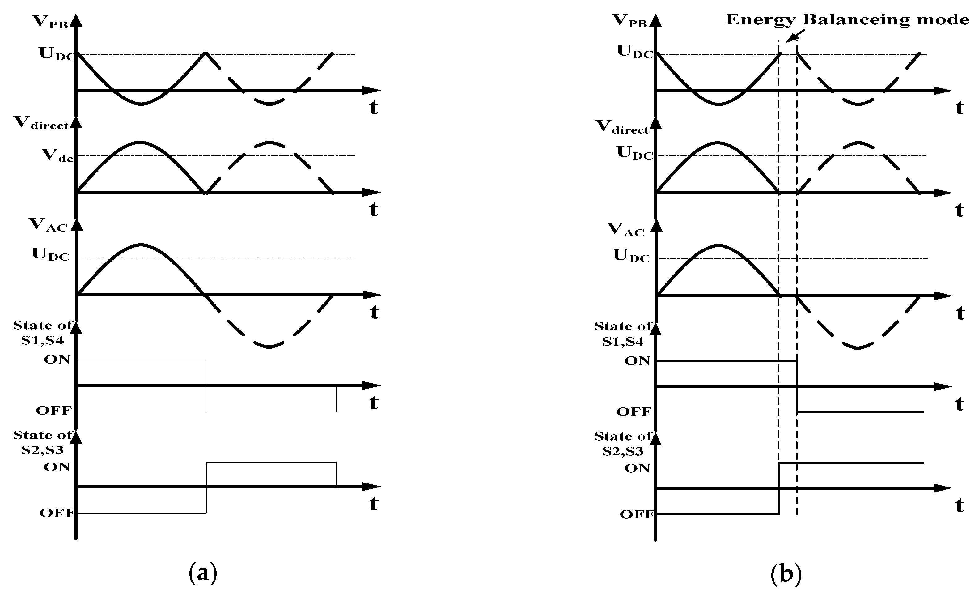
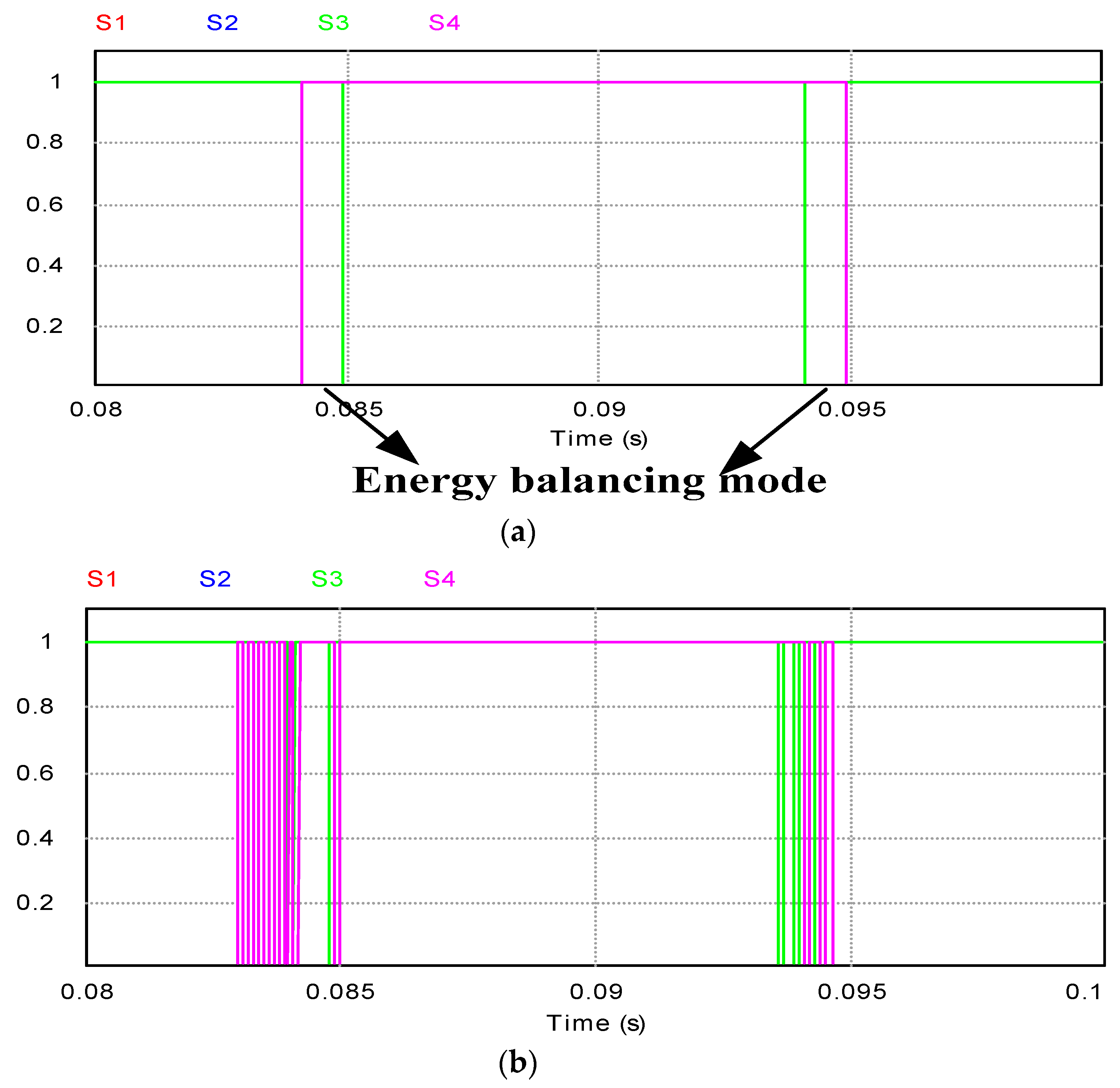
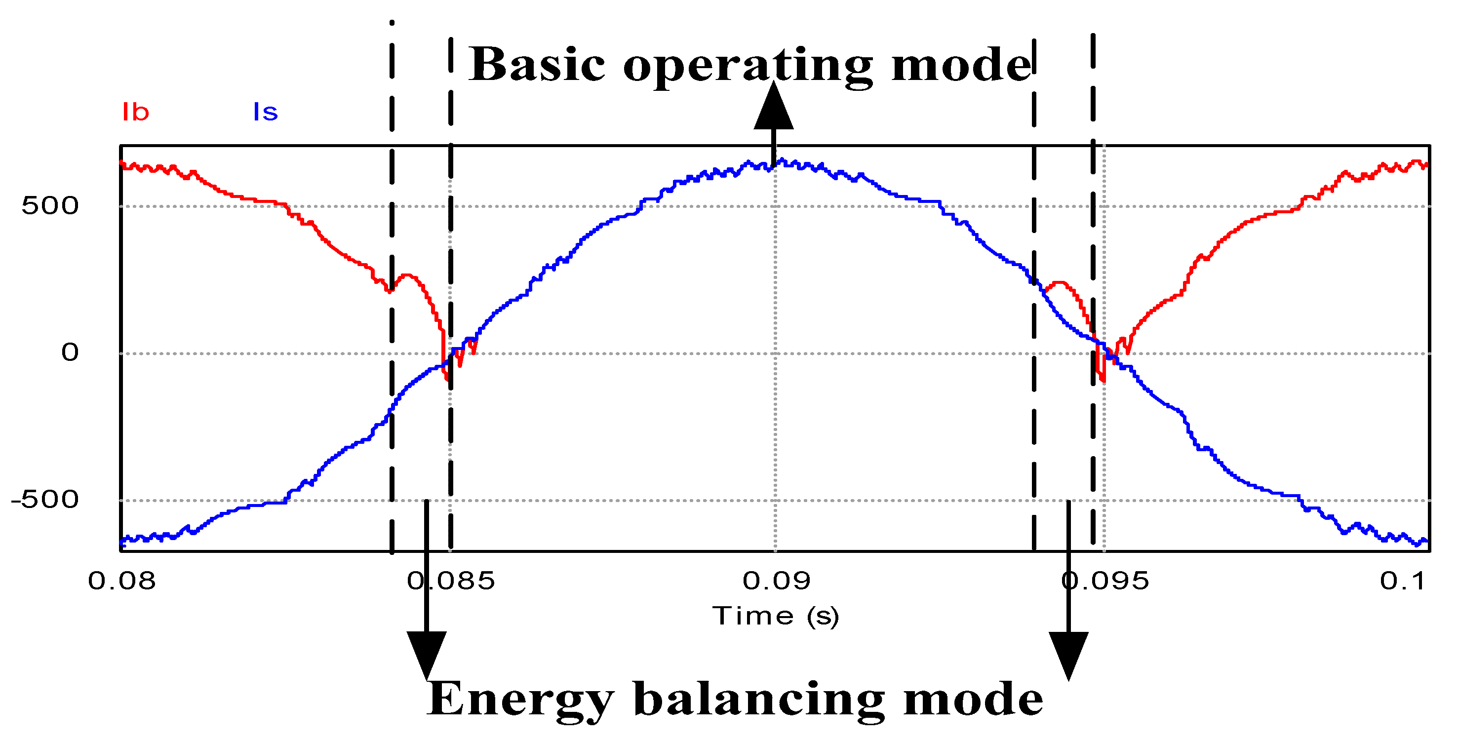
Energies 12 00091 g001
Figure 2. The voltage waveform and state of S1–S4: (a) without energy balance mode; (b) with energy balance mode.
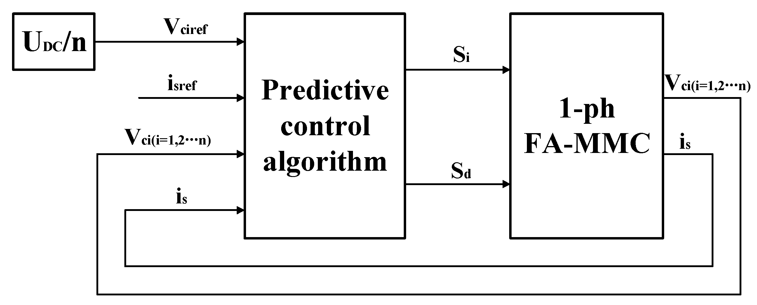
Energies 12 00091 g002
Figure 3. Block diagram of the predictive control strategy
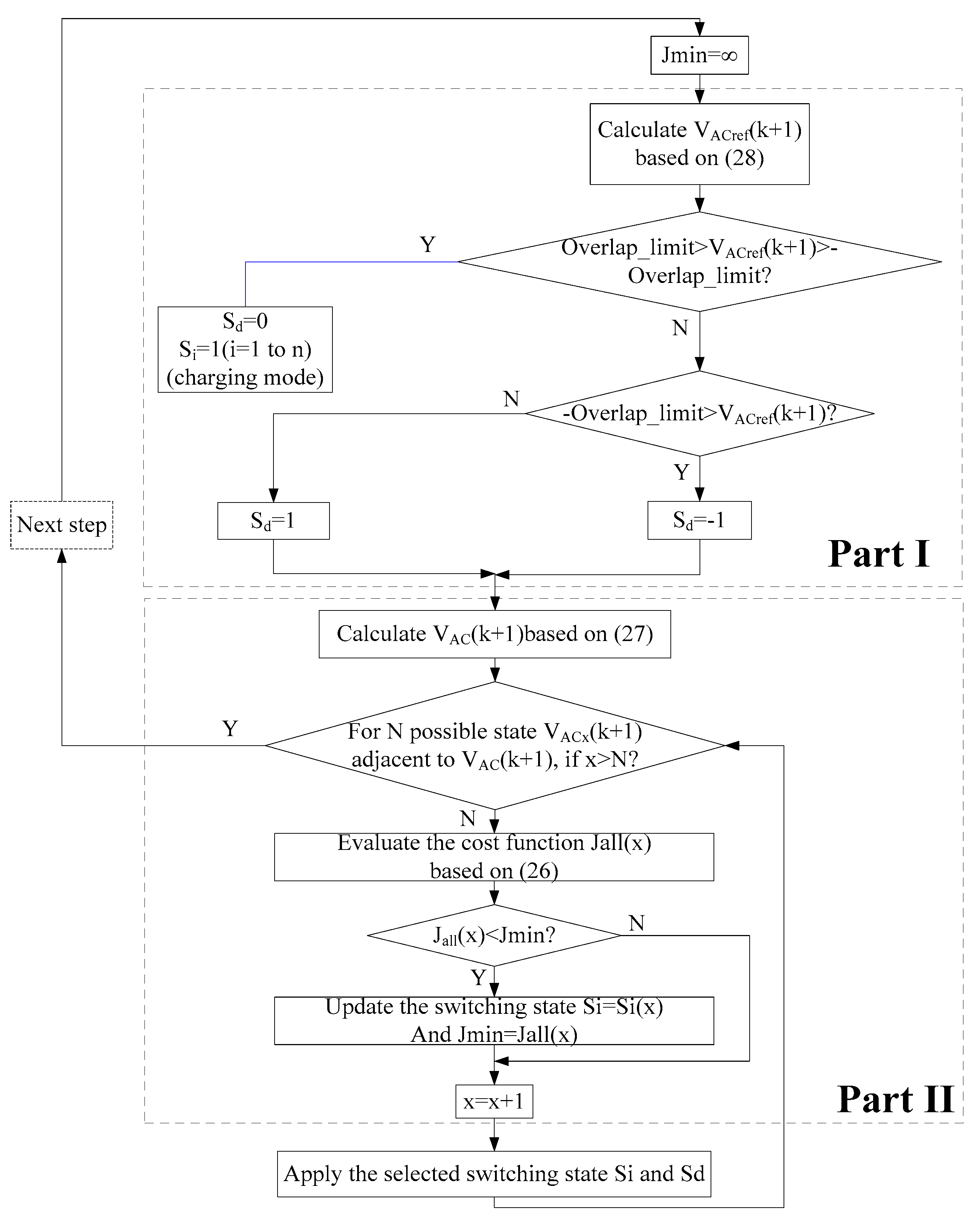
Energies 12 00091 g003
Figure 4. Schematic diagram of the control system.
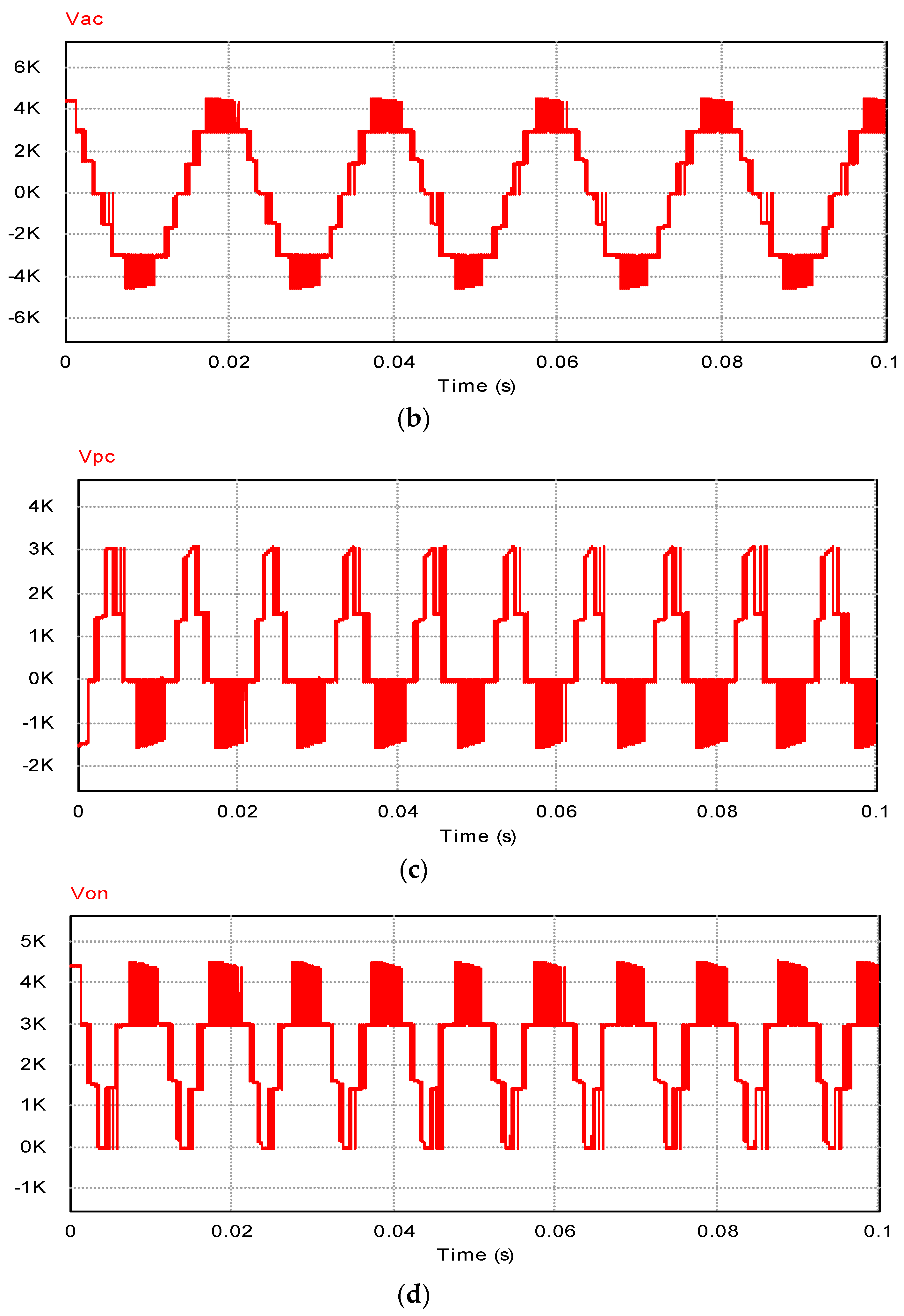
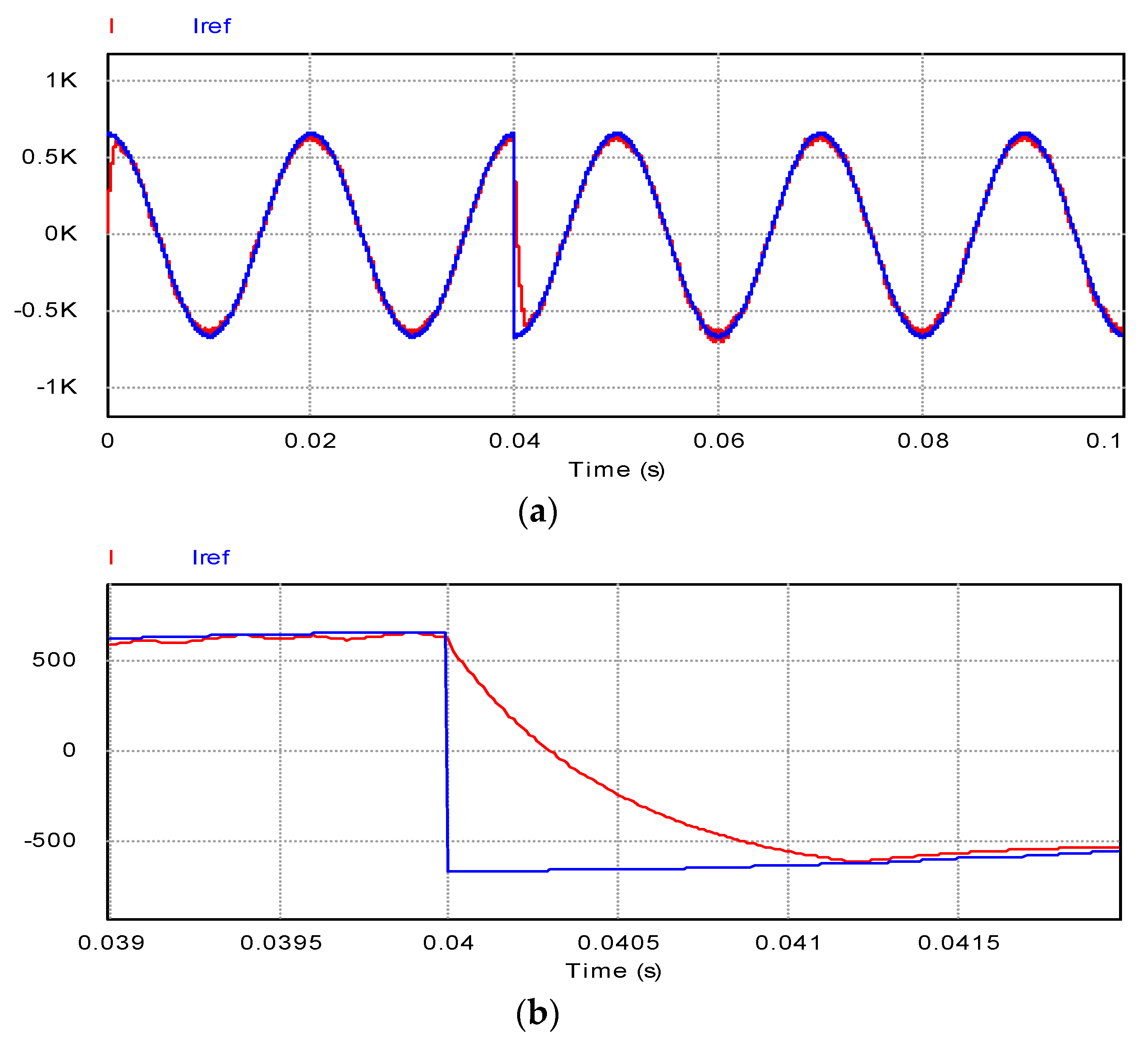
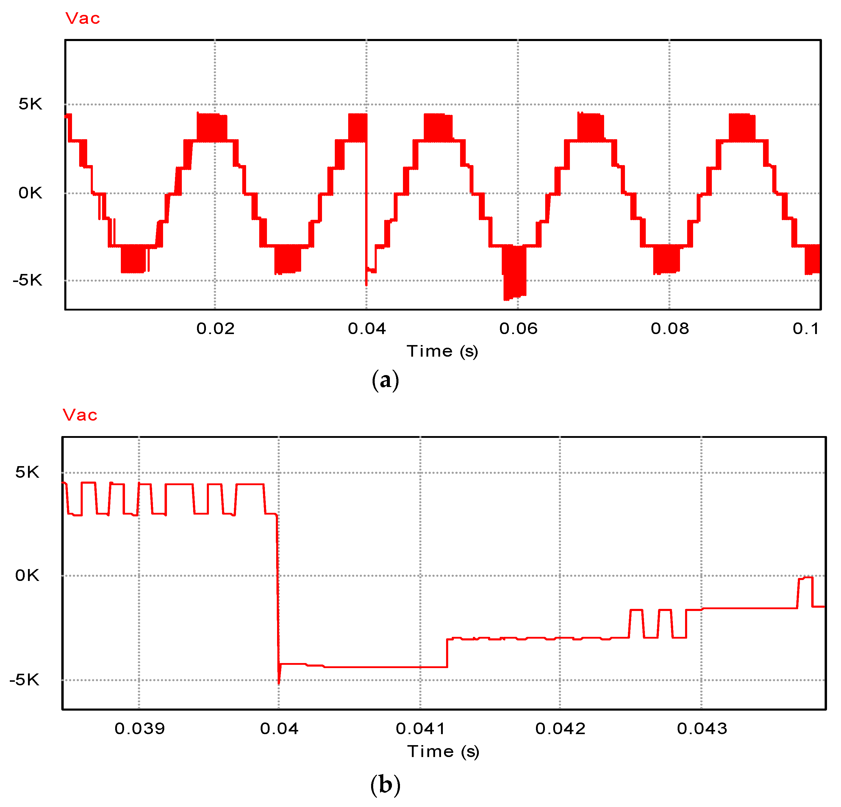
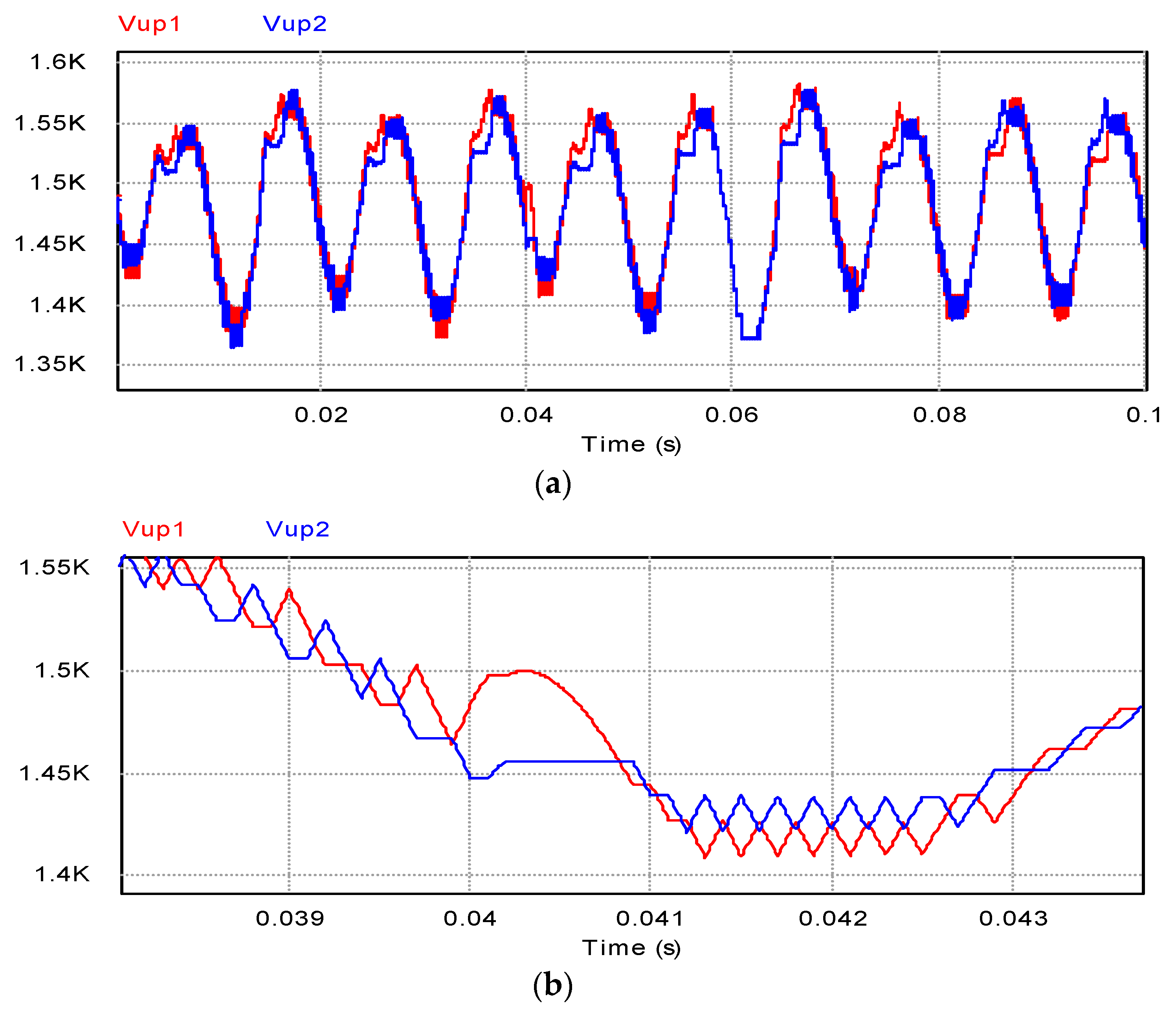
Energies 12 00091 g004
Figure 5. Simulation waveform of the single-phase FA-MMC in steady state operation: (a) Load current and reference current; (b) output AC voltage; (c) voltage of the stack of H-bridges; (d) voltage across the director switches S1–S4.
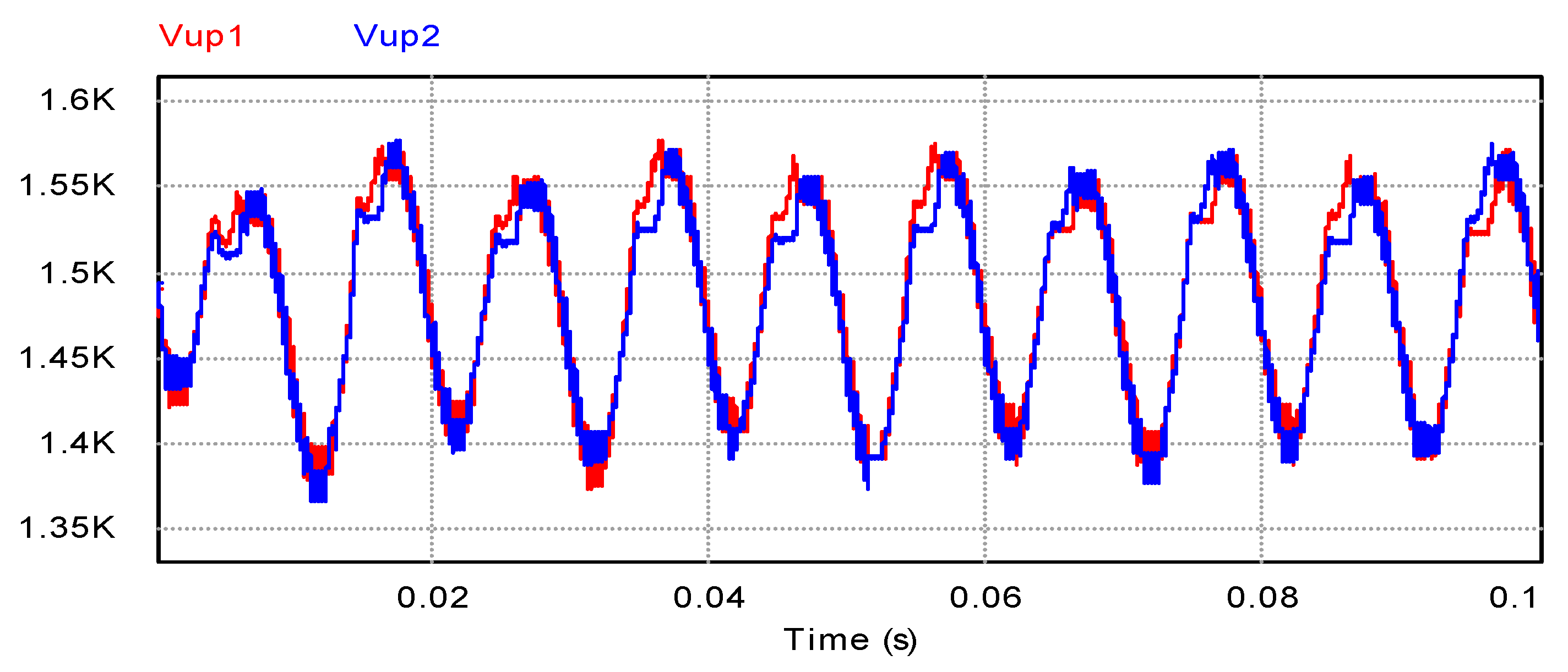
Energies 12 00091 g005aEnergies 12 00091 g005b
Figure 6. Capacitor voltages of the cells.
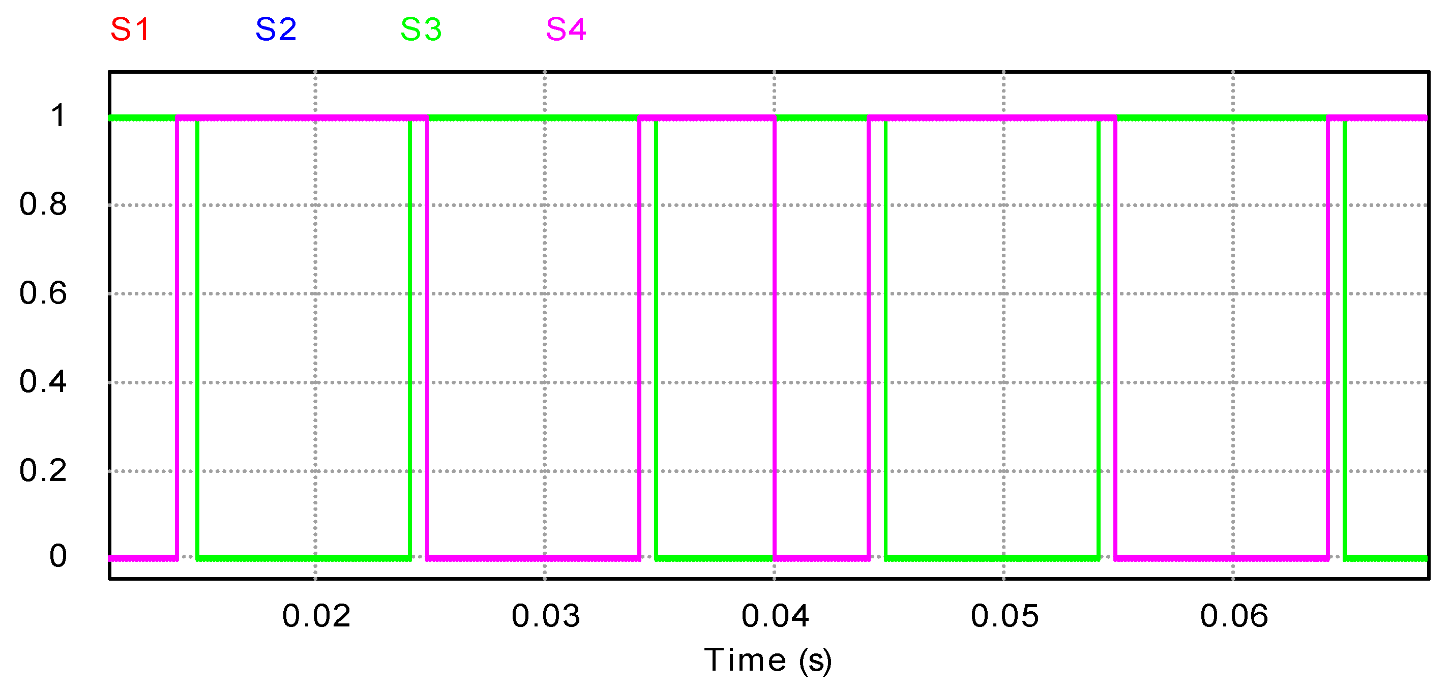
Energies 12 00091 g006
Figure 7. Director switch control signal of S1–S4: (a) Control signal based on Vacref(t+Ts); (b) control signal based on Vac(t + Ts).
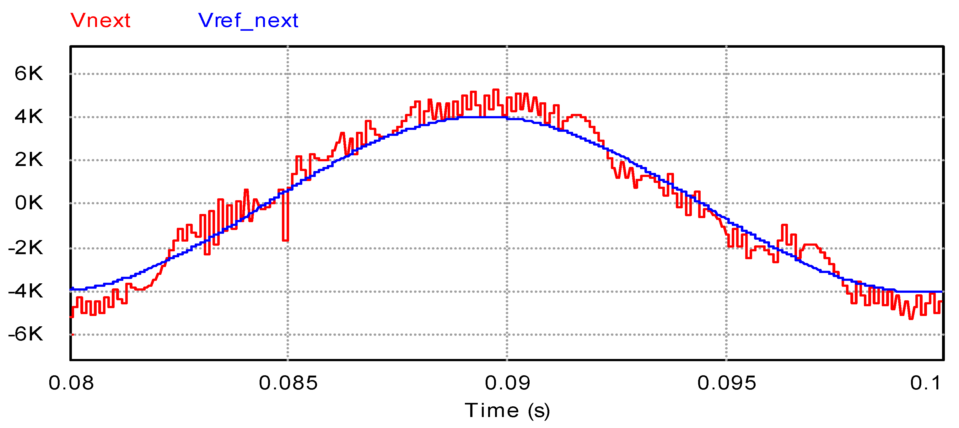
Energies 12 00091 g007
Figure 8. The waveforms of Vac and Vacref.
Energies 12 00091 g008
Figure 9. The waveforms of Vac and Vacref.
Energies 12 00091 g009
Figure 10. Load current for a sudden change: (a) reference current and actual load current; (b) Detail of the reference current and actual load current at the instant.
Energies 12 00091 g010
Figure 11. Output AC voltage waveforms: (a) Output AC voltage ; (b) detail of the output AC voltage at the instant.
Energies 12 00091 g011
Figure 12. Capacitor voltages of the sub-module.
Energies 12 00091 g012
Figure 13. Control signal of S1–S4.
Energies 12 00091 g013
Figure 14. Current and voltage simulation waveforms of a DC fault: (a) AC current; (b) DC current; (c) capacitor voltages.
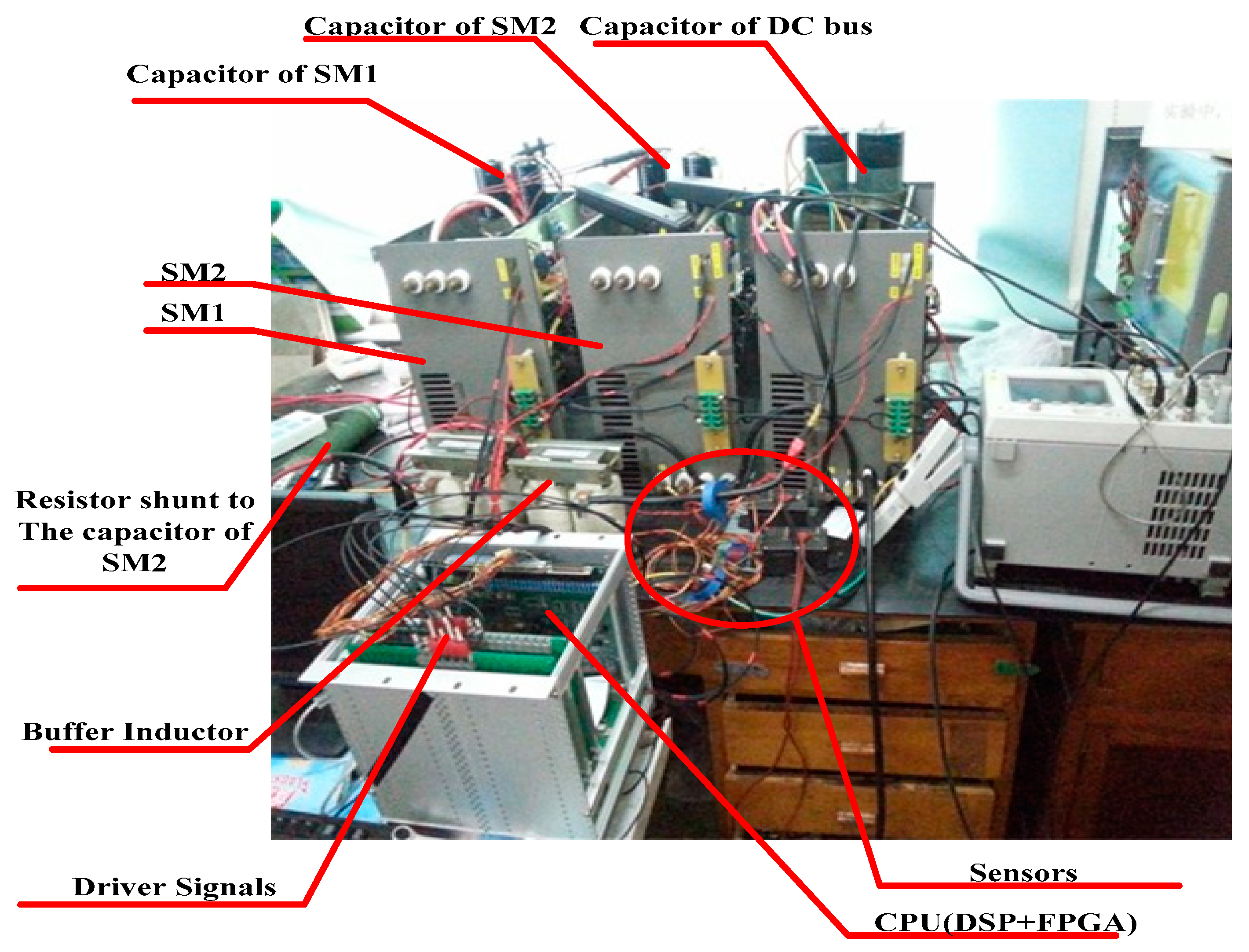
Energies 12 00091 g014aEnergies 12 00091 g014b
Figure 15. Photo of the modular multilevel converter (MMC)-based inverter for the experiment.
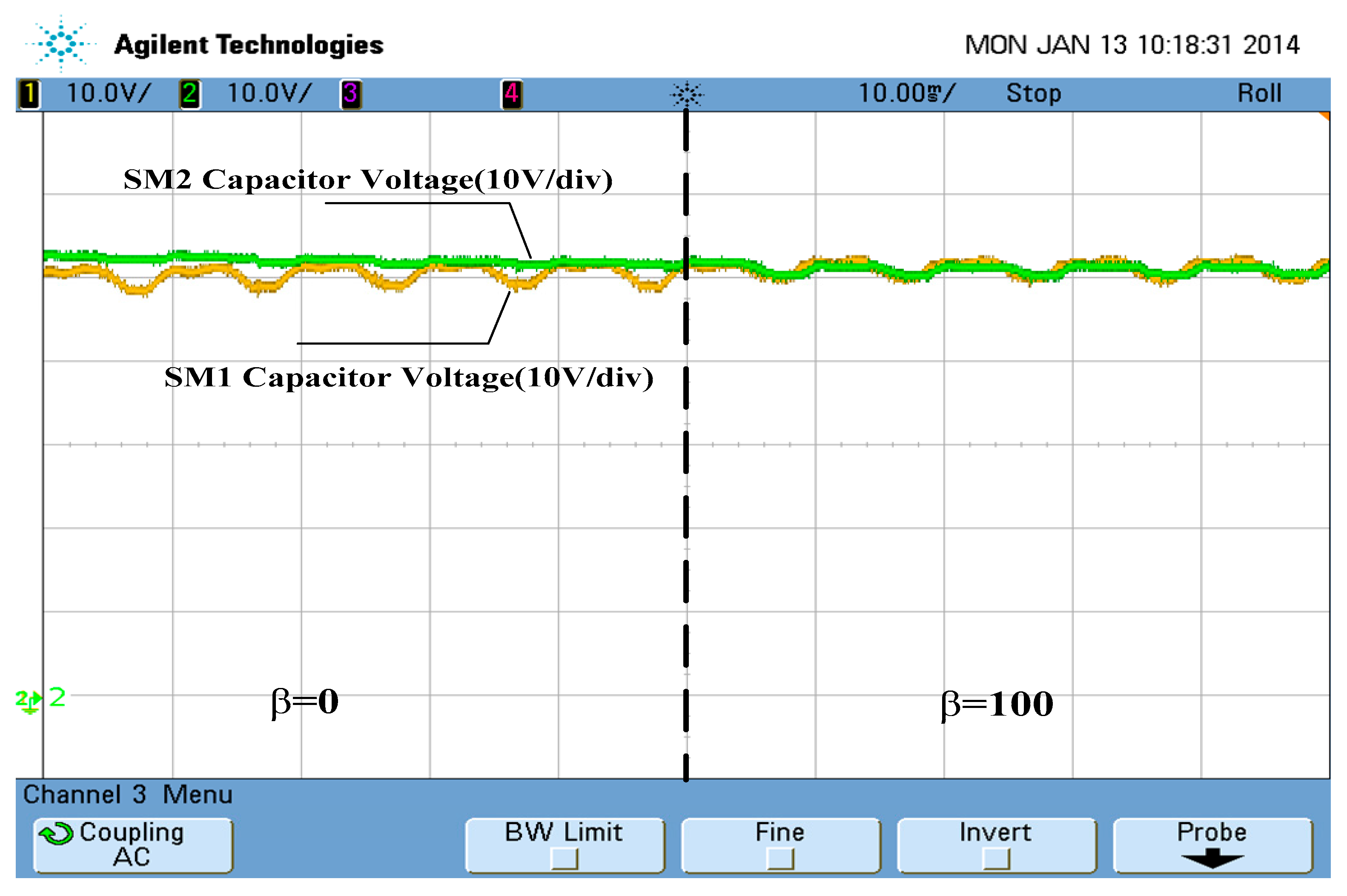
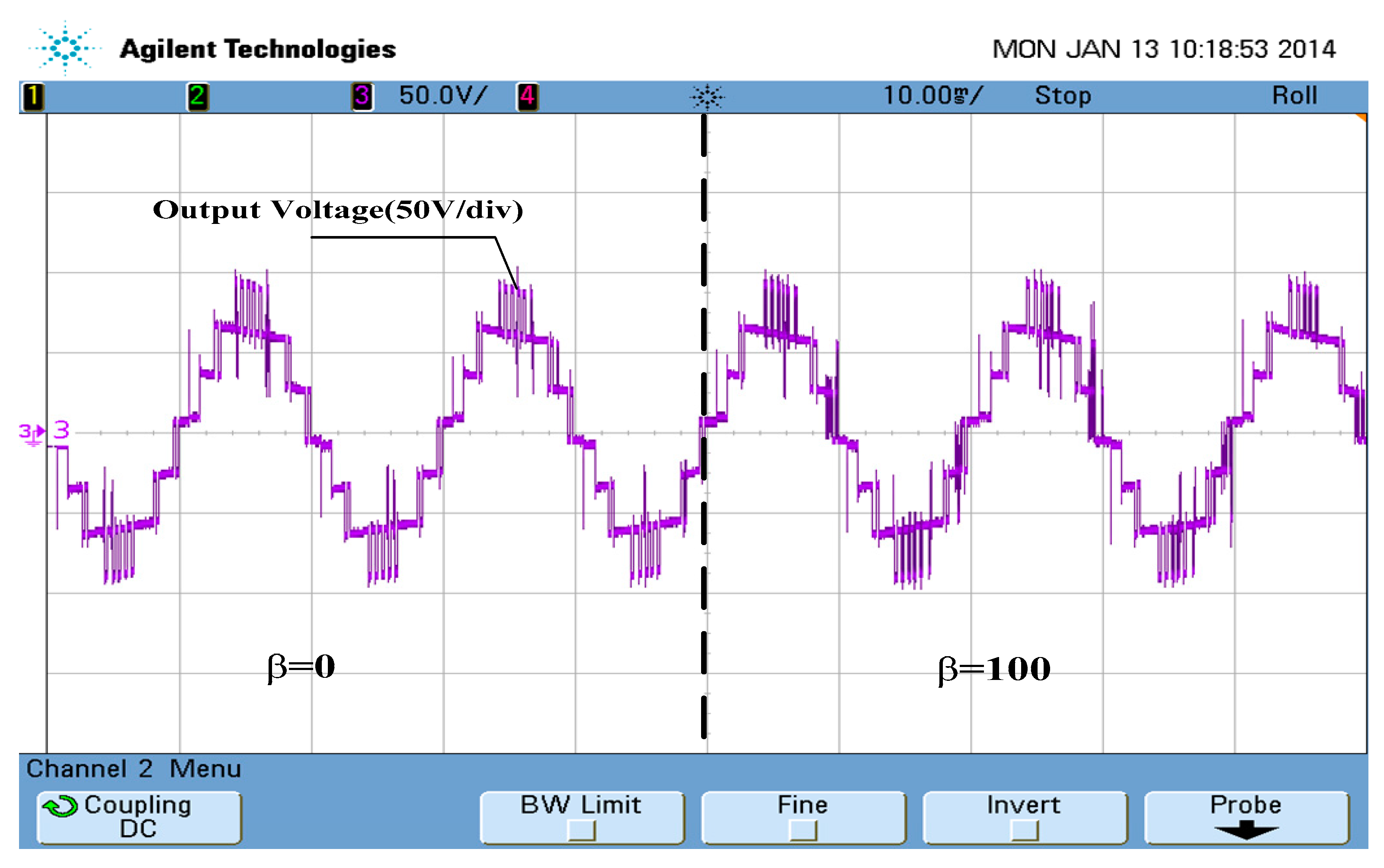
Energies 12 00091 g015
Figure 16. weighting factor β’s effects on the capacitor voltages.
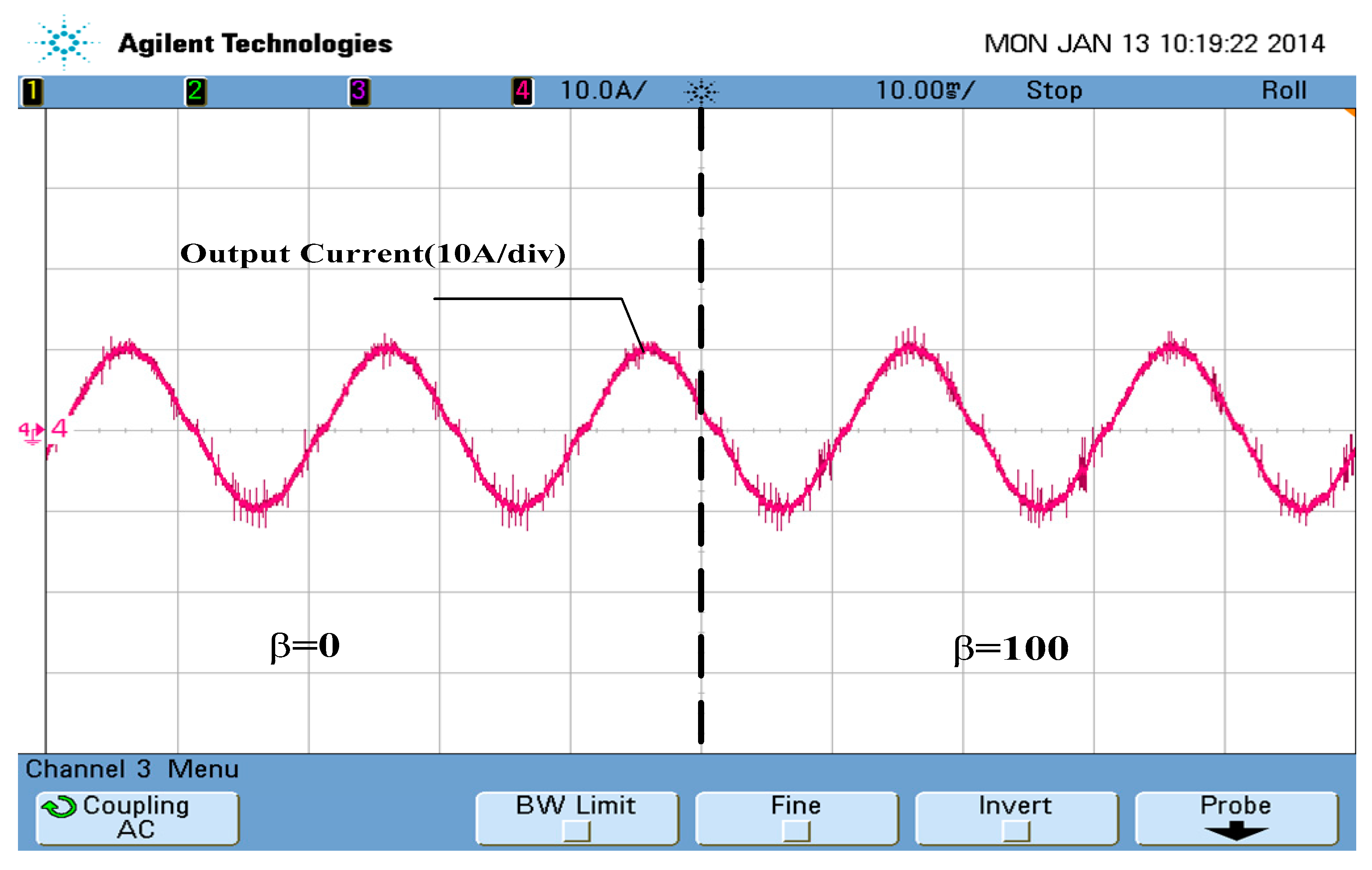
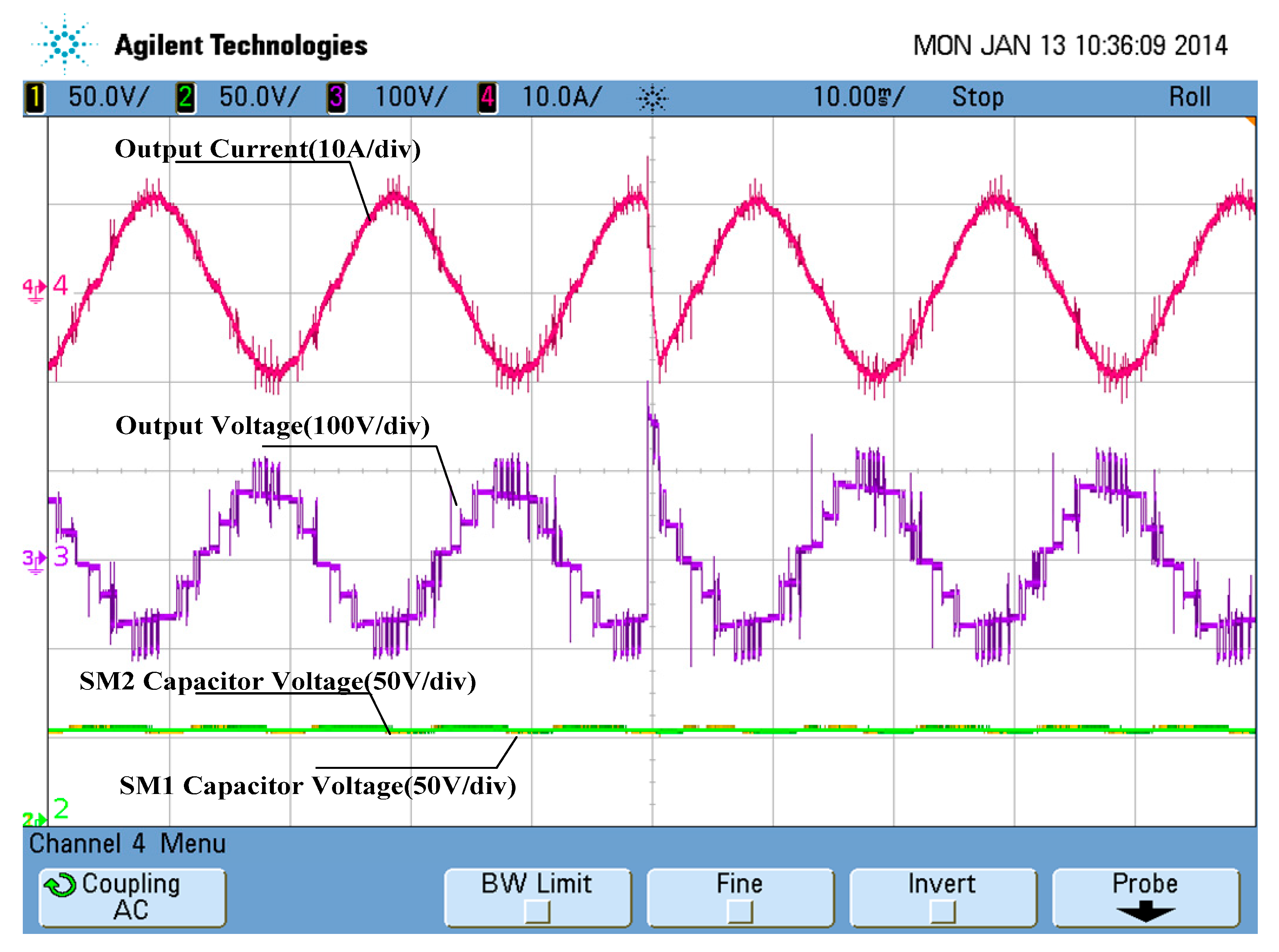
Energies 12 00091 g016
Figure 17. The waveform of the output current under balanced and unbalanced conditions.
Energies 12 00091 g017
Figure 18. The waveform of the output voltage under balanced and unbalanced conditions.
Energies 12 00091 g018
Figure 19. Waveform of the voltage and current for a step in the angle of the reference current.
Energies 12 00091 g019
Figure 20. Detail of the output voltage and current for a step in the angle of the reference current.
Energies 12 00091 g020
Figure 21. The equivalent circuit of the insulated-gate bipolar transistors (IGBTs) blocking when a DC fault occurs.
Energies 12 00091 g021
Table 1. Switching states of director switches.
ModeSdS1S2S3S4Output Voltage (VAC)
Basic Operating Mode1ONOFFOFFONVMN
−1OFFONONOFFVMN
Energy Balancing Mode0ONONONON0
0ONONOFFOFF0
0OFFOFFONON0
Table 2. Parameters of the study system of Figure 1b.
DC voltage UDC3000 V
Submodule capacitor C3300 μF
Load inductance Ls3 mH
Buffer inductors Lb0.1 mH
Load inductance R6
Sampling period Ts100 μs
Nominal frequencies f50 Hz
No. of cell in the stack of H-bridge cells2
Table 3. Experiment parameters.
DC voltage UDC100 V
Submodule capacitor C3300 μF
Load inductance Ls3 mH
Buffer inductors Lb0.1 mH
Load inductance R6
Sampling period Ts100 μs
Nominal frequencies f50 Hz
No. of cell in the stack of H-bridge cells2
Table 4. Number of semiconductor devices and sub-module capacitors.
TopologyNumber of Sub-Module CapacitorNumber of IGBTsNumber of Diodes
H-MMCN2 N0
F-MMCN4 N0
CH-MMCN2.35 N0.7 N
AAMC0.34 N1.8 N0
FA-MMC0.2 N1.6 N0
Table 5. Losses calculation results
TopologySwitching LossesConduction LossesTotal Losses
H-MMC0.29%0.82%1.11%
F-MMC0.29%1.88%2.18%
CH-MMC0.29%1.19%1.48%
AAMC0.16%0.47%0.63%
FA-MMC0.16%0.66%0.82%
Table 6. Comprehensive comparison with other various topology
TopologyEconomyEfficiencyVolumeDC Fault Blocking CapacityDemand for Insulation
H-MMC+++++++++
F-MMC++++++
CH-MMC++++++++
AAMC+++++++++++++++
FA-MMC+++++++++++++++++

