Article

Research on the Neutral-Point Voltage Balance for NPC Three-Level Inverters under Non-Ideal Grid Conditions

1
Nanjing University of Science and Technology, Nanjing 210094, China
2
Jiangsu Collaborative Innovation Center for Smart Distribution Network, Nanjing 211167, China
*
Author to whom correspondence should be addressed.
Energies 2018, 11(6), 1331; https://doi.org/10.3390/en11061331
Submission received: 8 April 2018 / Revised: 15 May 2018 / Accepted: 19 May 2018 / Published: 23 May 2018
(This article belongs to the Section F: Electrical Engineering)

Abstract

:
In order to solve the neutral-point voltage unbalancing problem for neutral-point clamped (NPC) three-level inverters under non-ideal grid conditions, a novel zero-sequence component injection method for modulation signals was proposed in this paper. Based on the mathematical expressions of neutral-point voltage unbalancing, the fluctuation of the neutral-point voltage under different grid conditions was studied. The proposed method dynamically calculates the zero-sequence component for modulation signals by region selections based on sinusoidal pulse width modulation (DCR-SPWM). Under non-ideal grid conditions, this DCR-SPWM method can control the neutral-point voltage balance for NPC three-level inverters with different grid and output power conditions, and improves the grid current quality. The simulation results verified the correctness of the theoretical analysis in this paper, and the feasibility and effectiveness of this method were verified by the experiments in the experimental platform of the NPC three-level grid-connected inverter based on DSP-CPLD controllers.

1. Introduction

The neutral-point clamped (NPC) three-level inverter has been widely used in medium or high voltage and high power conversions, especially as a dc/ac converter for a photovoltaic (PV) power generation system [1,2], which influences the safety and stability of the PV system for grid connection. Compared with two level inverters, the NPC three-level inverter has lower voltage stress on power devices, lower electromagnetic noise, and lower total harmonic distortion (THD) [3,4], which is shown in Figure 1.
In the NPC three-level inverter circuit, two capacitors for the dc bus are used in series to clamp the neutral-point (NP) potential. Ideally, the voltage of the two capacitors are both half of the dc bus voltage. However, due to the capacitance parameter error, the inconsistent characteristics of the switching devices, the unbalancing of three phase operation, etc. [5], the NP voltage unbalancing problem appears, which will increase the voltage stress on switching devices [6,7], and lead low-order harmonic currents into the grid [8]. Therefore, the NP voltage balance has been the research emphasis of three-level inverters.
Most of the research has focused on the NP voltage unbalancing problem under symmetrical load or ideal grid conditions. Based on space vector pulse width modulation (SVPWM), ref. [9] proposed a control strategy that replaced the small switching states with other switching states. Using sinusoidal pulse width modulation (SPWM), ref. [10] proposed a closed-loop space vector modulation using converter redundant switching states combined to the controller to balance the neutral point, and the dc link had very low voltage ripples due to lower harmonic components flowing through those capacitors via the harmonic current. In [11], a proportional integral (PI) controller was used to modify the reference current to maintain the NP voltage balance. NP balance methods based on zero-sequence component injection were proposed in [12,13], which calculated the zero-sequence component in the switching period. Based on the average NP voltage model in a line cycle, the PI controllers were proposed for the NP voltage balance in some papers, and the PI parameters for the controllers were usually selected for the maximum output power condition [14,15].
However, due to the nonlinear loads and transient grid faults, the three phase grid can become unbalanced and distorted [16,17,18]. Under the non-ideal conditions described above, the NP voltage module is different from that under ideal grid conditions, and the NP voltage unbalancing problem leads more low order harmonic currents into the grid [19,20], which significantly deteriorates the performance of the inverter. Therefore, as NP voltage balance methods designed under ideal grid conditions are not suitable for non-ideal grid conditions, it is important to research balancing the NP voltage under non-ideal grid conditions. Recently, some studies have focused on this problem. In [21,22], the redundant switching state was dictated based on the voltage feedback from the dc link to balance the NP voltage, which can balance the NP voltage under various load conditions with fast response and good dynamic performance. In [23,24], the expressions of NP voltage under unbalanced grid conditions were derived, and the relationship between the ripple of NP voltage and the unbalanced grid was studied. The authors in [20] analyzed the form and spectrums of NP voltage under low-voltage ride-through (LVRT) conditions, and proposed an optimized SVPWM method to control the NP voltage balance. In [25,26], the dc/dc converter was added to balance the NP voltage and suppress the common mode voltage under unbalanced grid conditions.
The objective of this paper was to propose a new method to control the NP voltage balance under non-ideal grid conditions. This method dynamically calculates the zero-sequence component for modulation signals by region selections based on SPWM (DCR-SPWM). Section 2 studies the NP voltage under different grid conditions and presents the expressions of NP voltage under non-ideal grid conditions. In Section 3, the DCR-SPWM method for non-ideal grid is proposed. Based on the mathematical expressions of NP voltage, the modulation signals are divided in different regions, and the expressions of zero-sequence component are derived, which is added to the modulation signals. Section 4 analyzes the NP voltage ripple and the harmonic performance of the grid currents with the DCR-SPWM method and compared it with the traditional SPWM method under different grid and output power conditions. Section 5 presents the simulated and experimental results of the proposed DCR-SPWM method and the method in [14] under different grid and output power conditions. The analysis and experiments showed that the DCR-SPWM method could control the NP voltage balance for NPC three-level inverters under non-ideal grid conditions, and improved the grid current quality.

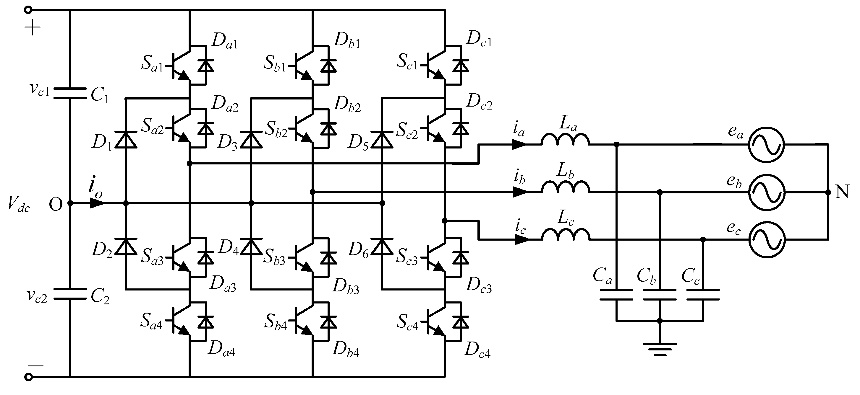
2. Mathematical Analysis of the Neutral-Point Voltage under Non-Ideal Grid Conditions

In Figure 1, vc1 is the voltage of capacitor C1, vc2 is the voltage of capacitor C2, and Vdc is the dc bus voltage. Supposing that vc1 and vc2 are equal, each phase leg of the NPC three-level inverter can output three levels (Vdc/2, −Vdc/2, 0), and the “P”, “N”, and “0” states represent Vdc/2, −Vdc/2, and 0, respectively.
In this paper, the SPWM method uses the single polar SPWM strategy, which is shown in Figure 2 where ux is the modulation signal of phase x (x = a, b, c) and vx is the leg voltage of phase x (x = a, b, c).
The NP current io can be defined as the average current in a switching cycle, which flows out from the neutral point O in Figure 1, it can be expressed as:
i o = x = a , b , c d x 0 i x
where dx0 and ix represent the duty cycle of “0” state and the three phase grid current, dx0 can be derived as:
{ d a 0 = 1 | u a _ r e f | d b 0 = 1 | u b _ r e f | d c 0 = 1 | u c _ r e f |
where ua_ref, ub_ref, uc_ref are three phase modulation signals. By substituting Equation (2) into Equation (1), io can be derived as:
i o = x = a , b , c | u x _ r e f | i x
Defining vc as the difference between vc1 and vc2 in Figure 1, vc is expressed as:
v c = v c 1 v c 2
Meanwhile, the NP voltage vc can be expressed as:
v c = 1 C i o d t
where C is the capacitance of C1 and C2.
Substituting Equation (3) into Equation (5), vc can be derived as:
v c = 1 C ( x = a , b , c | u x _ r e f | i x ) d t
Under the non-ideal grid condition, according to the symmetrical components method, three phase unbalance components are composed with symmetrical positive/negative/zero-sequence components. As the zero-sequence component can be neglected in the Three-phase Three-wire inverter system, therefore, the modulation signals can be expressed as:
{ u a _ r e f = u a p _ r e f + u a n _ r e f u b _ r e f = u b p _ r e f + u b n _ r e f u c _ r e f = u c p _ r e f + u c n _ r e f
where uap_ref, ubp_ref, ucp_ref represent the positive-sequence components of three phase modulation signals and uan_ref, ubn_ref, ucn_ref represent the negative-sequence components of three phase modulation signals.
Commonly, to describe the proportion of negative-sequence component to the positive-sequence component for the non-ideal grid, the unbalance factor λ is introduced here [27]:
λ = A n A p
where Ap and An represent the amplitudes of positive and negative sequence components, respectively.
Supposing that the voltage of the filter inductor is ignored, the positive-sequence and negative-sequence components of three phase modulation signals can be expressed as:
{ u a p _ r e f = 2 E m p V d c sin ( ω t + φ u p ) u b p _ r e f = 2 E m p V d c sin ( ω t + φ u p 2 π / 3 ) u c p _ r e f = 2 E m p V d c sin ( ω t + φ u p + 2 π / 3 )
{ u a n _ r e f = λ 2 E m p V d c sin ( ω t + φ u n ) u b n _ r e f = λ 2 E m p V d c sin ( ω t + φ u n + 2 π / 3 ) u c n _ r e f = λ 2 E m p V d c sin ( ω t + φ u n 2 π / 3 )
In Equations (9) and (10), Emp represents the amplitude of the positive-sequence grid voltages; ω is the line angle frequency; and φup and φun represent the phase angle of positive-sequence and negative-sequence modulation signals, respectively, which also represent the phase angle of positive-sequence and negative-sequence grid voltages, respectively.
Under non-ideal grid conditions, unbalance grid voltages cause a double line frequency ripple at the output power of the inverter [28]. If the control target of the grid side is suppressing the ripple component at active power, the three phase grid currents can be expressed as:
{ i a = i a p + i a n i b = i b p + i b n i c = i c p + i c n
where iap, ibp, icp represent the positive-sequence components of three phase grid currents and ian, ibn, icn represent the negative-sequence components of three phase grid currents.
In Equation (11), the positive-sequence and negative-sequence components of three phase grid currents are as follows:
{ i a p = I m p sin ( ω t + φ u p φ u i ) i b p = I m p sin ( ω t + φ u p φ u i 2 π / 3 ) i c p = I m p sin ( ω t + φ u p φ u i + 2 π / 3 )
{ i a n = λ I m p sin ( ω t + φ u n φ u i ) i b n = λ I m p sin ( ω t + φ u n φ u i + 2 π / 3 ) i c n = λ I m p sin ( ω t + φ u n φ u i 2 π / 3 )
In Equations (12) and (13), Imp represents the amplitude of the positive-sequence grid currents, and φui is the phase difference between positive-sequence grid voltage and positive-sequence grid current.
Substituting Equations (7) and (11) into Equation (6), vc can be derived as:
v c = 1 C [ x = a , b , c | u x p _ r e f + u x n _ r e f | ( i x p + i x n ) ] d t
By substituting Equations (9), (10), (12), and (13) into Equation (14), the waveforms of vc under different grid conditions are shown in Figure 3, where C and Imp are normalized.
Under ideal grid condition (λ = 0) in Figure 3, it can be seen that vc fluctuates at three times the line frequency. Under non-ideal grid conditions, when λ = 0.1, the fluctuating frequency of vc changes to the line frequency, and the ripple of vc is also larger than that under ideal grid conditions.

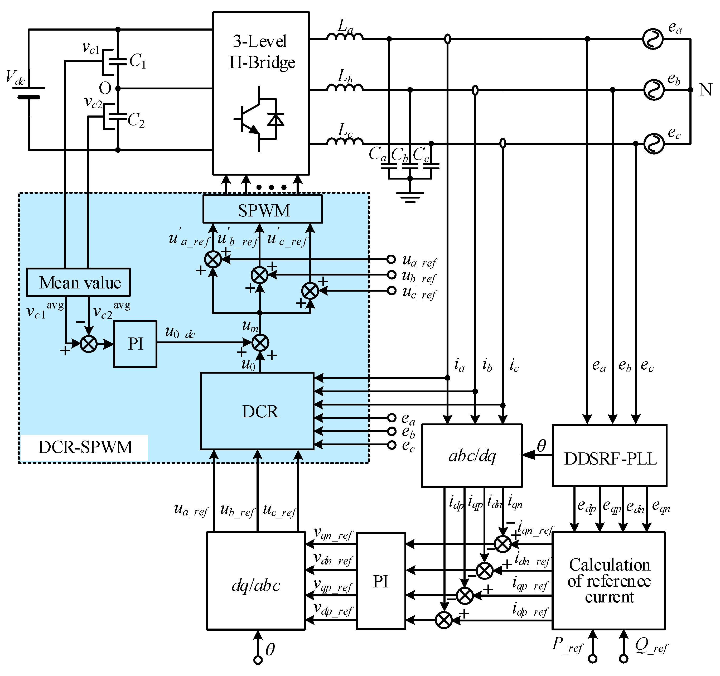
3. Proposed NP Voltage Balance Method under Non-Ideal Grid Conditions

In Section 2, from Equation (14), it can be seen that the fluctuation of NP voltage is caused by the NP current io. Therefore, by adding the appropriate zero-sequence component into the modulation signals, io can be controlled, then the NP voltage balance can be achieved.

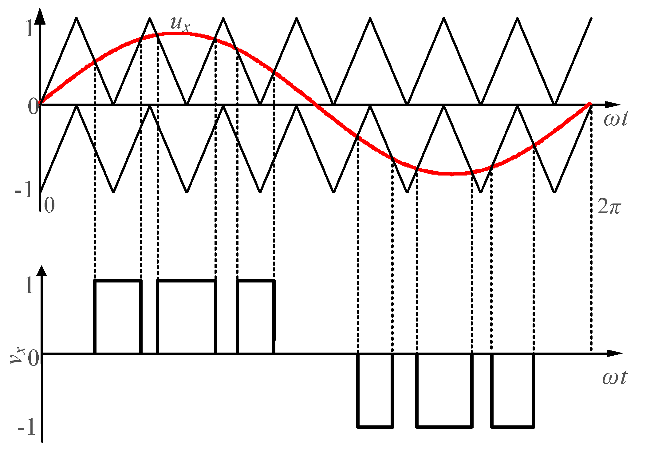
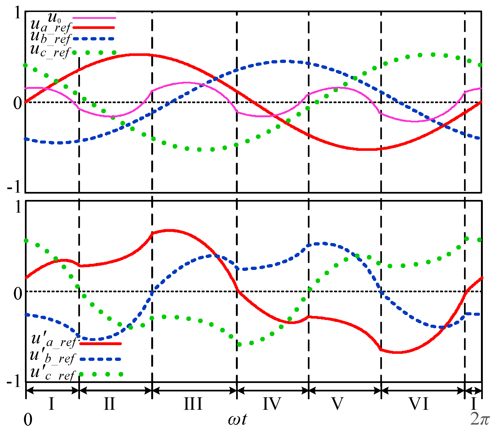
3.1. Analysis of Zero-Sequence Component for Modulation Signals

Defining u0 as the zero-sequence component, which is added to the modulation signals, three phase modulation signals can be expressed as:
{ u a _ r e f = u a p _ r e f + u a n _ r e f + u 0 u b _ r e f = u b p _ r e f + u b n _ r e f + u 0 u c _ r e f = u c p _ r e f + u c n _ r e f + u 0
By substituting Equations (11) and (15) into Equation (3), the expression of io is derived as:
i o = x = a , b , c [ | u x p _ r e f + u x n _ r e f + u 0 | ( i x p + i x n ) ]
Defining φ’ua0, φ’ub0, φ’uc0 as the positively sloped zero-crossing points s of ua_ref, ub_ref, uc_ref, respectively. Aiming at eliminating the ripple of NP voltage, io is controlled to be zero in Equation (16), when φ’ua0 > 0, u0 can be expressed as:
u 0 = { ( u a p _ r e f + u a n _ r e f ) ( i a p + i a n ) ( u b p _ r e f + u b n _ r e f ) ( i b p + i b n ) + ( u c p _ r e f + u c n _ r e f ) ( i c p + i c n ) ( i a p + i a n ) ( i b p + i b n ) + ( i c p + i c n ) ,   φ u a 0 ω t < φ u c 0 π ( u a p _ r e f + u a n _ r e f ) ( i a p + i a n ) ( u b p _ r e f + u b n _ r e f ) ( i b p + i b n ) ( u c p _ r e f + u c n _ r e f ) ( i c p + i c n ) ( i a p + i a n ) ( i b p + i b n ) ( i c p + i c n ) ,   φ u c 0 π ω t < φ u b 0 ( u a p _ r e f + u a n _ r e f ) ( i a p + i a n ) + ( u b p _ r e f + u b n _ r e f ) ( i b p + i b n ) ( u c p _ r e f + u c n _ r e f ) ( i c p + i c n ) ( i a p + i a n ) + ( i b p + i b n ) ( i c p + i c n ) ,   φ u b 0 ω t < φ u a 0 + π ( u a p _ r e f + u a n _ r e f ) ( i a p + i a n ) + ( u b p _ r e f + u b n _ r e f ) ( i b p + i b n ) ( u c p _ r e f + u c n _ r e f ) ( i c p + i c n ) ( i a p + i a n ) + ( i b p + i b n ) ( i c p + i c n ) ,   φ u a 0 + π ω t < φ u c 0 ( u a p _ r e f + u a n _ r e f ) ( i a p + i a n ) + ( u b p _ r e f + u b n _ r e f ) ( i b p + i b n ) + ( u c p _ r e f + u c n _ r e f ) ( i c p + i c n ) ( i a p + i a n ) + ( i b p + i b n ) + ( i c p + i c n ) ,   φ u c 0 ω t < φ u b 0 + π ( u a p _ r e f + u a n _ r e f ) ( i a p + i a n ) ( u b p _ r e f + u b n _ r e f ) ( i b p + i b n ) + ( u c p _ r e f + u c n _ r e f ) ( i c p + i c n ) ( i a p + i a n ) ( i b p + i b n ) + ( i c p + i c n ) ,   φ u b 0 + π ω t < 2 π 0 ω t < φ u a 0
When φ’ua0 < 0, u0 can be expressed as:
u 0 = { ( u a p _ r e f + u a n _ r e f ) ( i a p + i a n ) ( u b p _ r e f + u b n _ r e f ) ( i b p + i b n ) + ( u c p _ r e f + u c n _ r e f ) ( i c p + i c n ) ( i a p + i a n ) ( i b p + i b n ) + ( i c p + i c n ) ,   φ u a 0 + 2 π ω t < 2 π 0 ω t < φ u c 0 π ( u a p _ r e f + u a n _ r e f ) ( i a p + i a n ) ( u b p _ r e f + u b n _ r e f ) ( i b p + i b n ) ( u c p _ r e f + u c n _ r e f ) ( i c p + i c n ) ( i a p + i a n ) ( i b p + i b n ) ( i c p + i c n ) ,   φ u c 0 π ω t < φ u b 0 ( u a p _ r e f + u a n _ r e f ) ( i a p + i a n ) + ( u b p _ r e f + u b n _ r e f ) ( i b p + i b n ) ( u c p _ r e f + u c n _ r e f ) ( i c p + i c n ) ( i a p + i a n ) + ( i b p + i b n ) ( i c p + i c n ) ,   φ u b 0 ω t < φ u a 0 + π ( u a p _ r e f + u a n _ r e f ) ( i a p + i a n ) + ( u b p _ r e f + u b n _ r e f ) ( i b p + i b n ) ( u c p _ r e f + u c n _ r e f ) ( i c p + i c n ) ( i a p + i a n ) + ( i b p + i b n ) ( i c p + i c n ) ,   φ u a 0 + π ω t < φ u c 0 ( u a p _ r e f + u a n _ r e f ) ( i a p + i a n ) + ( u b p _ r e f + u b n _ r e f ) ( i b p + i b n ) + ( u c p _ r e f + u c n _ r e f ) ( i c p + i c n ) ( i a p + i a n ) + ( i b p + i b n ) + ( i c p + i c n ) ,   φ u c 0 ω t < φ u b 0 + π ( u a p _ r e f + u a n _ r e f ) ( i a p + i a n ) ( u b p _ r e f + u b n _ r e f ) ( i b p + i b n ) + ( u c p _ r e f + u c n _ r e f ) ( i c p + i c n ) ( i a p + i a n ) ( i b p + i b n ) + ( i c p + i c n ) ,   φ u b 0 + π ω t < φ u a 0 + 2 π  
The positively sloped zero-crossing points φ’ua0, φ’ub0, φ’uc0 can be expressed as:
φ u a 0 = 1 2 [ arcsin ( C a A a 2 + B a 2 ) arctan ( B a A a ) ]
φ u b 0 = 1 2 [ arcsin ( C b A b 2 + B b 2 ) arctan ( B b A b ) ]
φ u c 0 = 1 2 [ arcsin ( C c A c 2 + B c 2 ) arctan ( B c A c ) ]
In Equations (19)–(21), the expressions of coefficients Ai, Bi, Ci, (i = a, b, c) are shown in Table 1.
As shown in Figure 4, when Emp/(Vdc/2) = 0.5, λ = 0.1, and φui = −π/4, u0 is calculated in different regions I–VI, which is divided by the zero-crossing points of ux_ref (x = a, b, c).

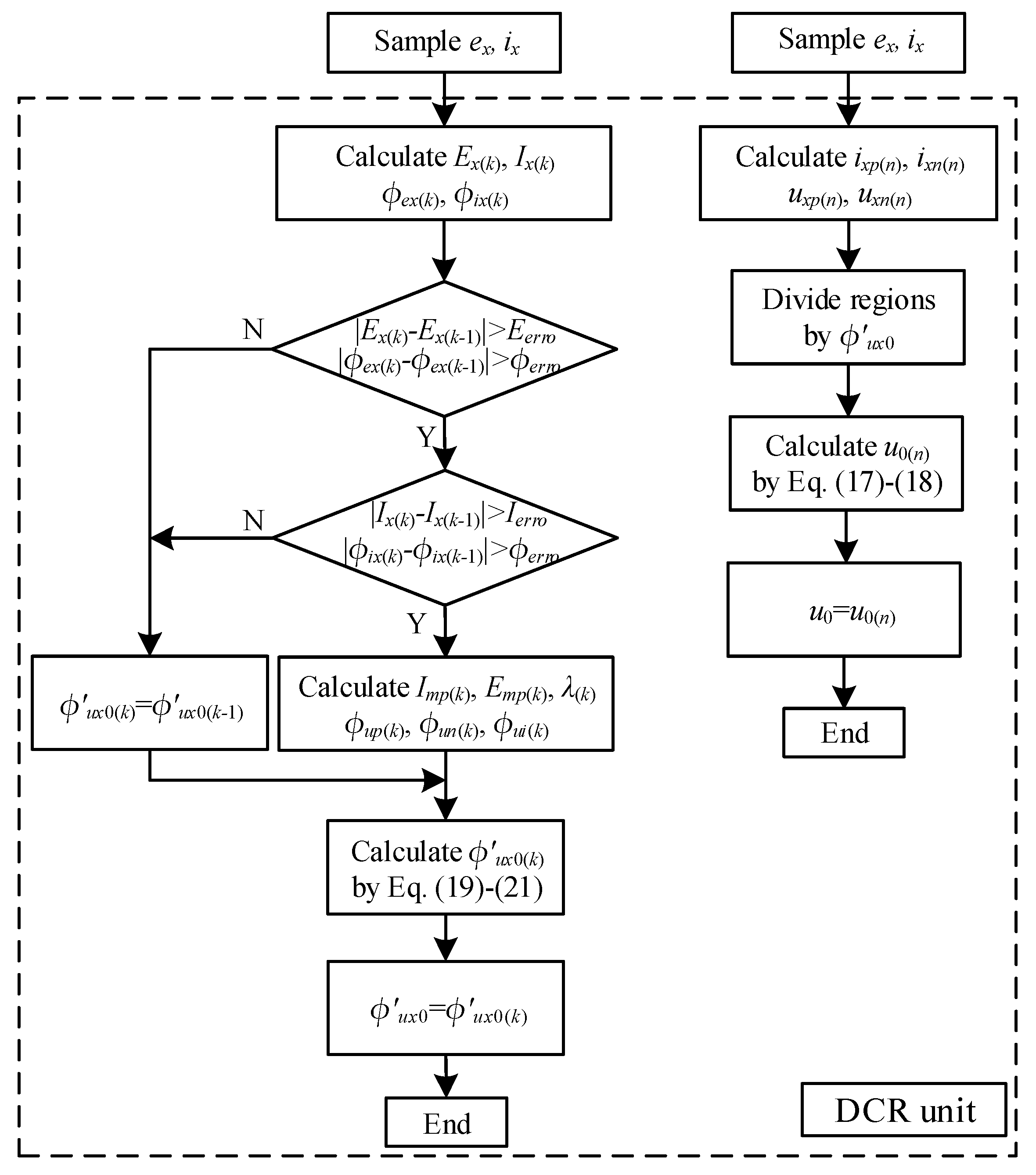
3.2. Design of the NP Voltage Balance Controller

The control principle diagram of the NPC three-level grid-connected inverter under non-ideal grid conditions is shown in Figure 5, where the DDSRF-PLL represents the decoupling double synchronous reference frame phase-locked loop unit, and the DCR unit dynamically calculates the zero-sequence component for modulation signals by region selections (DCR).
In Figure 5, according to three phase modulation signals ua_ref, ub_ref, uc_ref, three phase grid voltages ea, eb, ec, grid currents ia, ib, ic and average capacitor voltages vc1avg, vc2avg, the DCR-SPWM block generates the modified modulation signals with zero-sequence voltage um for balancing the NP voltage, where vc1avg, vc2avg are the average voltage of vc1 and vc2 in a line cycle. Additionally, ua_ref, ub_ref, uc_ref are the modified modulation signals with um, which are compared with carrier waves to generate driving signals for the switches of the inverter.
Inside the DCR-SPWM block, the input signals ua_ref, ub_ref, uc_ref of the DCR unit are modulation signals without zero-sequence voltage, ia, ib, ic are three phase grid currents, ea, eb, ec are three phase grid voltages, and the output signals u0 of the DCR unit is the zero-sequence component for the modulation signals, which are used for suppressing the ripple of the NP voltage vc.
In order to eliminate the ripple of the NP voltage vc, the DCR unit dynamically calculates the zero-sequence component u0 in different regions of the modulation signal, which is divided by the positively sloped zero-crossing points φ’ux0 of ux_ref (x = a, b, c), where φ’ux0 is calculated according to the grid currents and grid voltages at different grid conditions in a line cycle. The detailed flowchart of the DCR unit is shown in Figure 6. Furthermore, a PI controller is used to restrain the dc unbalanced voltage of vc, and the input signals of the PI controller are vc1avg, vc2avg. The design of this controller for the NP voltage balance has been previously presented in many papers, so the detailed design is not given here. In order to make the difference between vc1avg and vc2avg zero, this controller outputs the signal u0_dc, which is added to the modulation signals. Therefore, um is the sum of u0_dc and u0, which is the zero-sequence voltage that is added to the modulation signals to balance the NP voltage.
Figure 6 shows the main working flowchart of the DCR unit where Ex (x = a, b, c) and Ix represent the root mean square (RMS) value of the grid voltages ex and grid currents ix, respectively, φex and φix represent the phase angle of grid voltages and grid currents, respectively. φ’ux0(k) and u0(n) are the calculated value of φ’ux0 and u0, respectively. Eerro, Ierro, and φerro are allowable errors, Emp and Imp are the amplitudes of positive-sequence grid voltages and positive-sequence grid currents, respectively, φup and φun are the phase angles of the positive-sequence and negative-sequence modulation signals, respectively, φui is the phase difference between the positive-sequence grid voltage and positive-sequence grid current, λ is the unbalance factor, ixp and ixn represent the positive-sequence and negative-sequence components of three phase grid currents, and uxp and uxn represent the positive-sequence and negative-sequence components of the three phase modulation signals.
In the k-th line cycle, the RMS value Ex(k), Ix(k), and phase angle φex(k), φix(k) are calculated, and are compared with Ex(k − 1), Ix(k − 1), φex(k − 1), and φix(k − 1), respectively, which are the calculated values in the (k − 1)th line cycle. If the absolute differences between the values of variables in the kth and (k − 1)th line cycle are greater than the allowable errors, the positively sloped zero-crossing points φ’ux0(k) of ux_ref (x = a, b, c) need to be calculated by Equations (19)–(21), if not, φ’ux0(k) of ux_ref (x = a, b, c) are equal to φ’ux0(k − 1) of ux_ref (x = a, b, c), which are calculated in the (k − 1)th line cycle. In the nth switching cycle, uxp(n), uxn(n), ixp(n), and ixn(n) are calculated, and a line cycle is divided into six regions I-VI by φ’ux0, then u0(n) is calculated by Equations (17) and (18) in the present region.

4. Performance Analysis

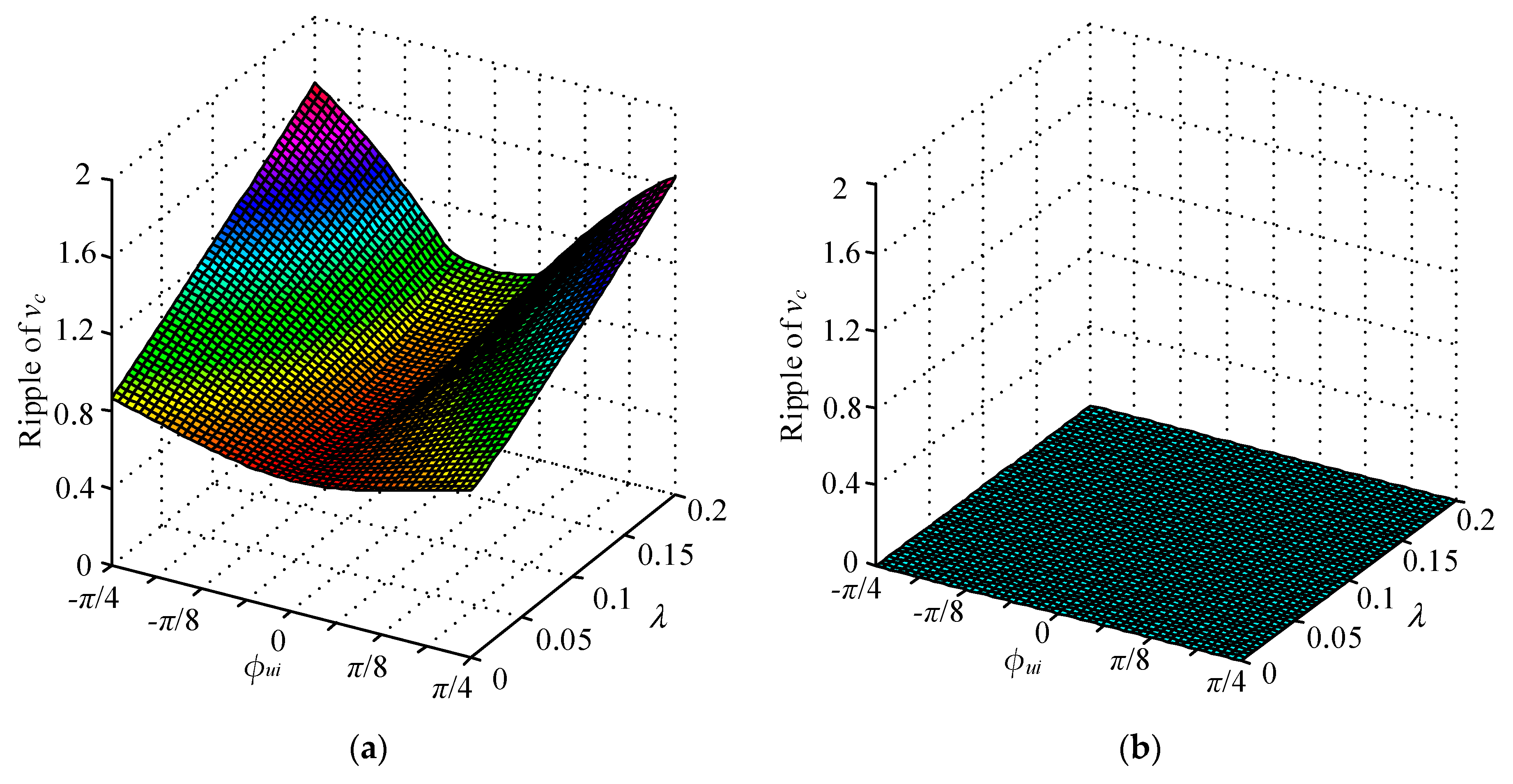
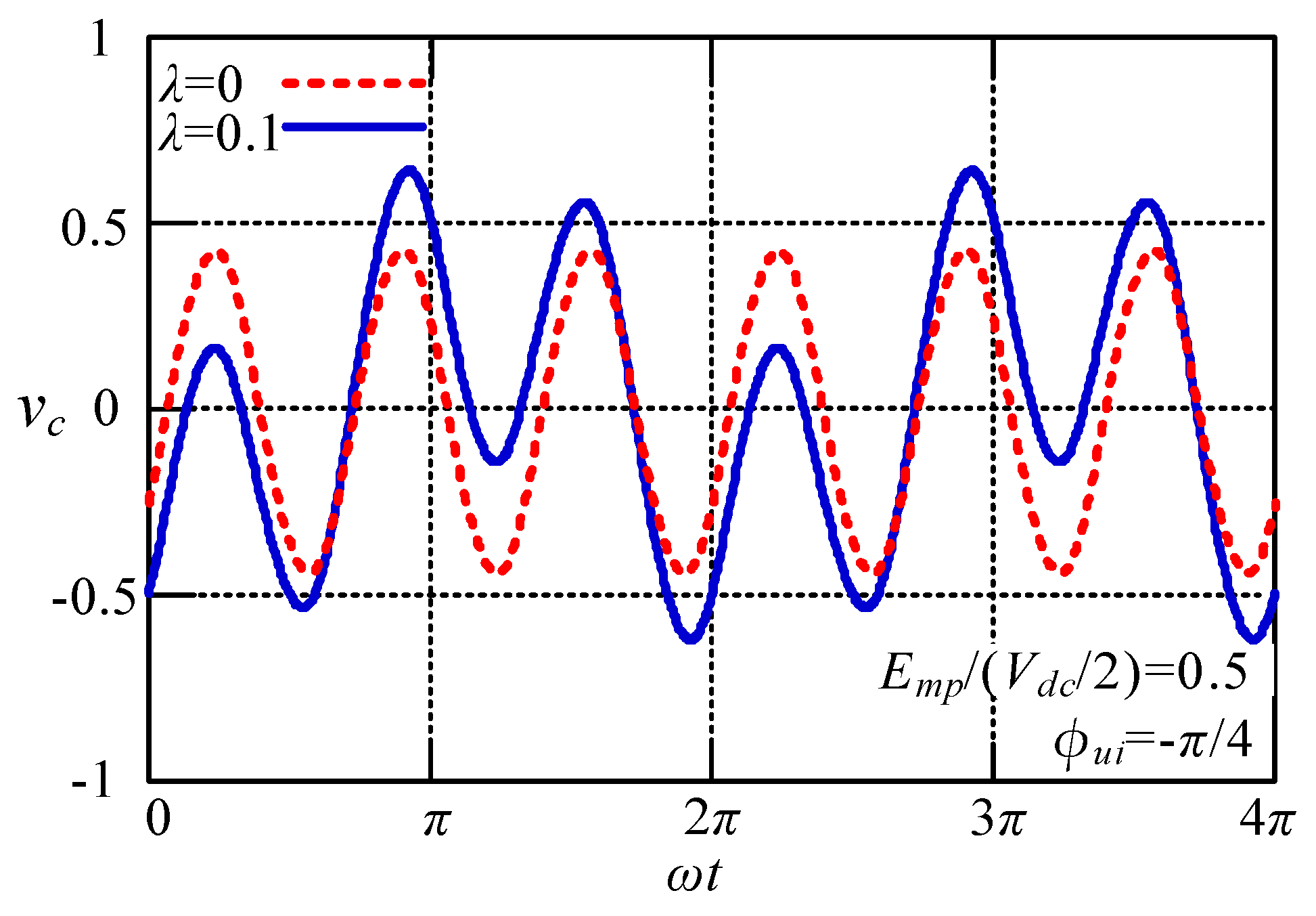
4.1. Analysis of the NP Voltage Fluctuation

According to Equations (6) and (16), when the proposed DCR-SPWM method is applied, vc can be expressed as:
v c = 1 C [ x = a , b , c | u x p _ r e f + u x n _ r e f + u 0 | ( i x p + i x n ) ] d t
Supposing that Emp/(Vdc/2) = 0.5, C, and Imp are normalized, according to Equations (9)–(14) and (22), the ripple of vc is related to λ and φui. With the traditional SPWM and proposed DCR-SPWM method, surfaces for the ripple of vc are plotted as shown in Figure 7.
In Figure 7a, with the traditional SPWM method, the ripple of vc increases when φui varies from 0 to π/4 (or −π/4 to 0), and λ varies from 0 to 0.2. In Figure 7b, with the proposed DCR-SPWM method, the ripple of vc is almost zero, which is not varied with φui and λ.
From the comparison above, it can be seen that the proposed DCR-SPWM method can suppress the NP voltage ripple under different λ and φui conditions.

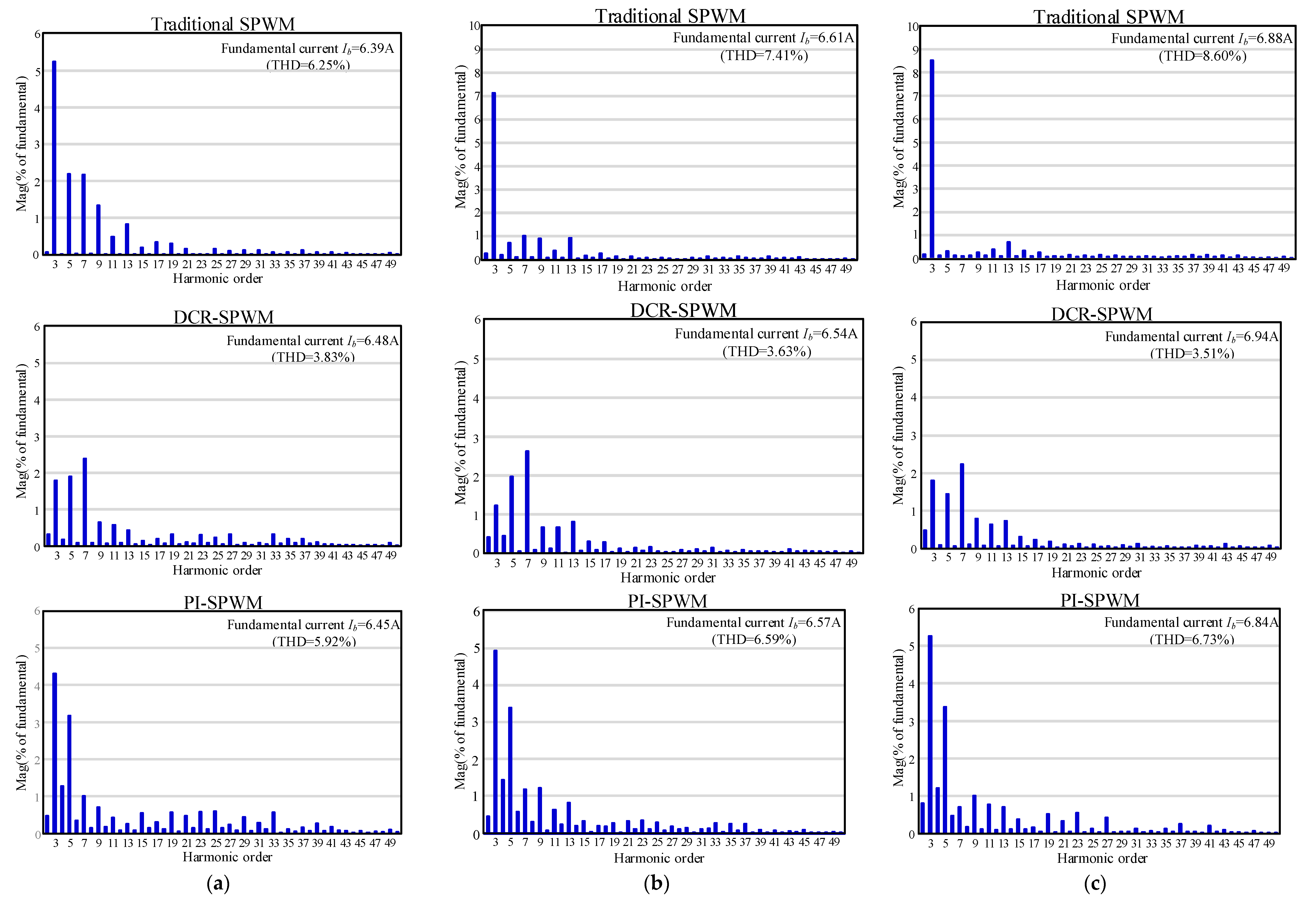
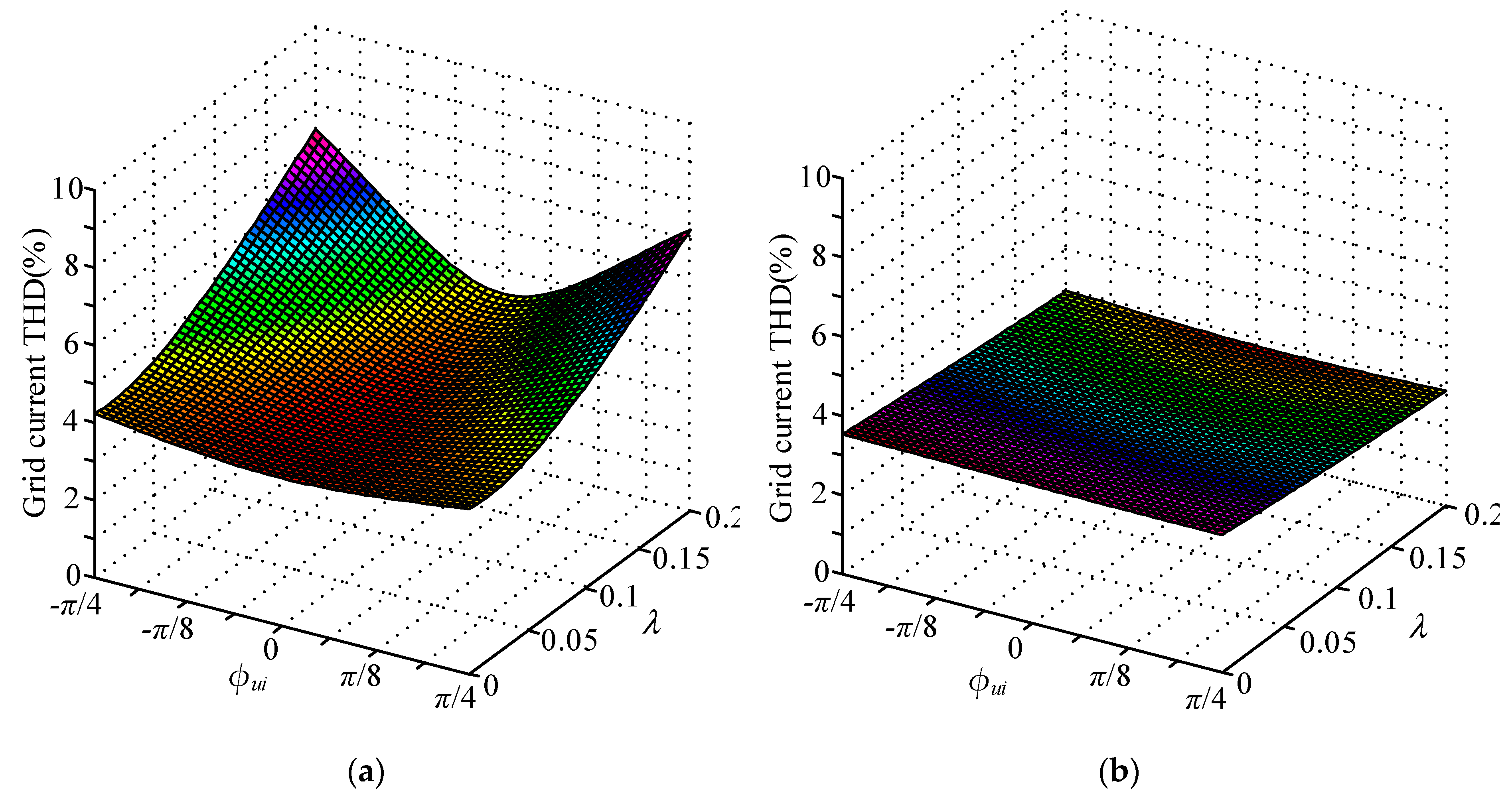
4.2. Analysis of the Grid Current Harmonics

Suppose that vx_SPWM and vx_DCR are the leg voltages of the inverter with the traditional SPWM and proposed DCR-SPWM method, respectively, considering the influence of NP voltage, vx_SPWM and vx_DCR are expressed as follows:
v x _ S P W M = ( u x p _ r e f + u x n _ r e f ) V d c 2 + | u x p _ r e f + u x n _ r e f | v c 2 + v xh _ mod
v x _ D C R = ( u x p _ r e f + u x n _ r e f + u 0 ) V d c 2 + | u x p _ r e f + u x n _ r e f + u 0 | v c 2 + v xh _ mod
In Equations (23) and (24), vxh_mod represents the harmonic component caused by the modulation method, which was analyzed in [29].
In the Three-phase Three-wire inverter system, the grid currents of the inverter can be expressed as:
i x = 1 L [ v x e x 1 3 x = a , b , c ( v x + e x ) ] d t
where L is inductance of the filter inductor, and the THD value of the grid currents can be calculated as per [29]:
THD = 0 2 π i x 2 ( ω t ) d ω t 0 2 π i x 1 2 ( ω t ) d ω t 1
where ix1 represents the fundamental component of the grid currents.
According to Equations (9)–(14) and (22)–(26), the THD value of the grid currents is related to λ and φui. The surfaces for THD of grid current ib with the traditional SPWM and DCR-SPWM method are shown in Figure 8. Compared with the traditional SPWM method, the THD value was lower when the proposed DCR-SPWM method was applied, and was lower than 4% under different λ and φui conditions.
From the analysis above, it can be seen that the proposed DCR-SPWM method can improve the quality of grid currents under different λ and φui conditions.

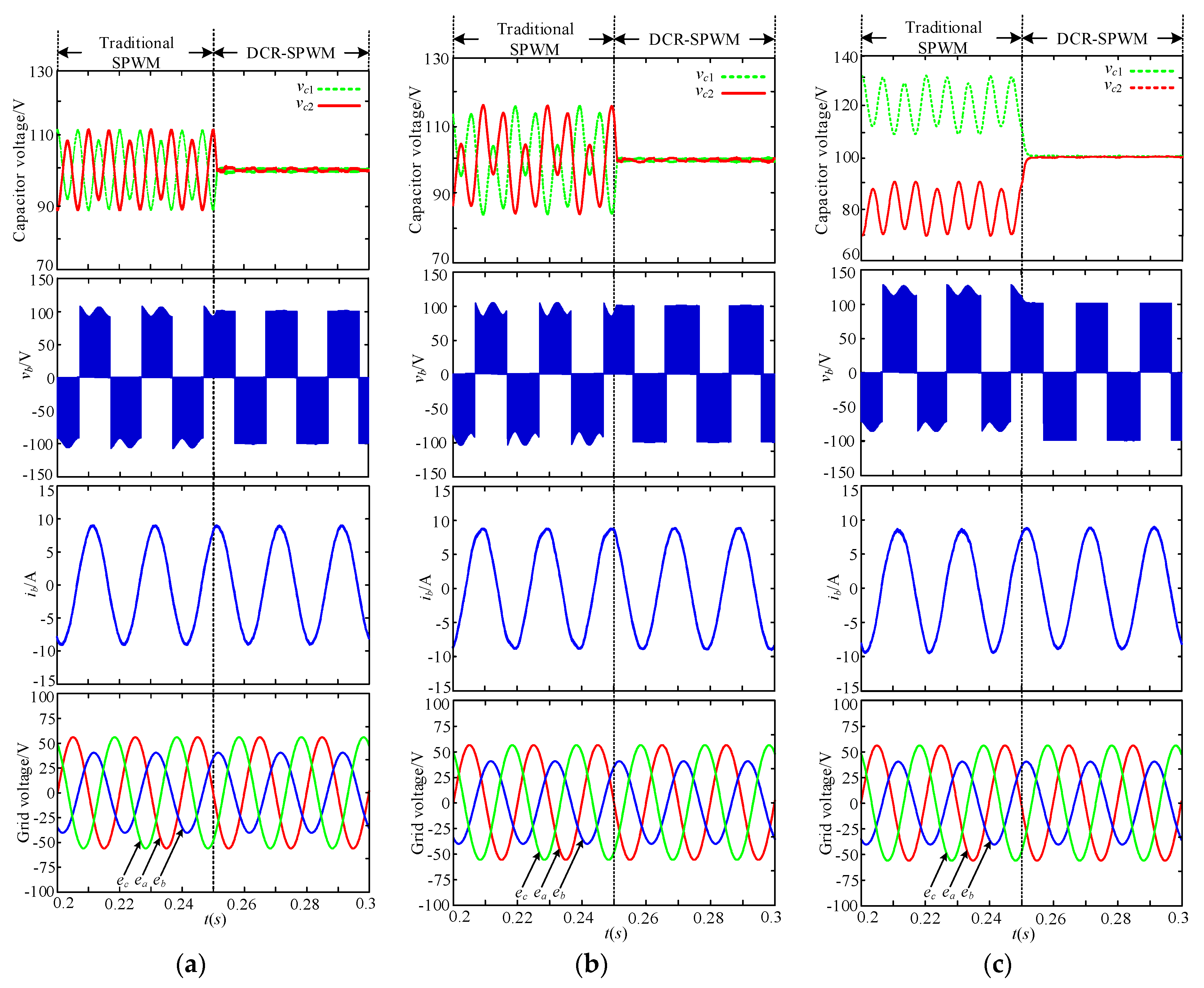
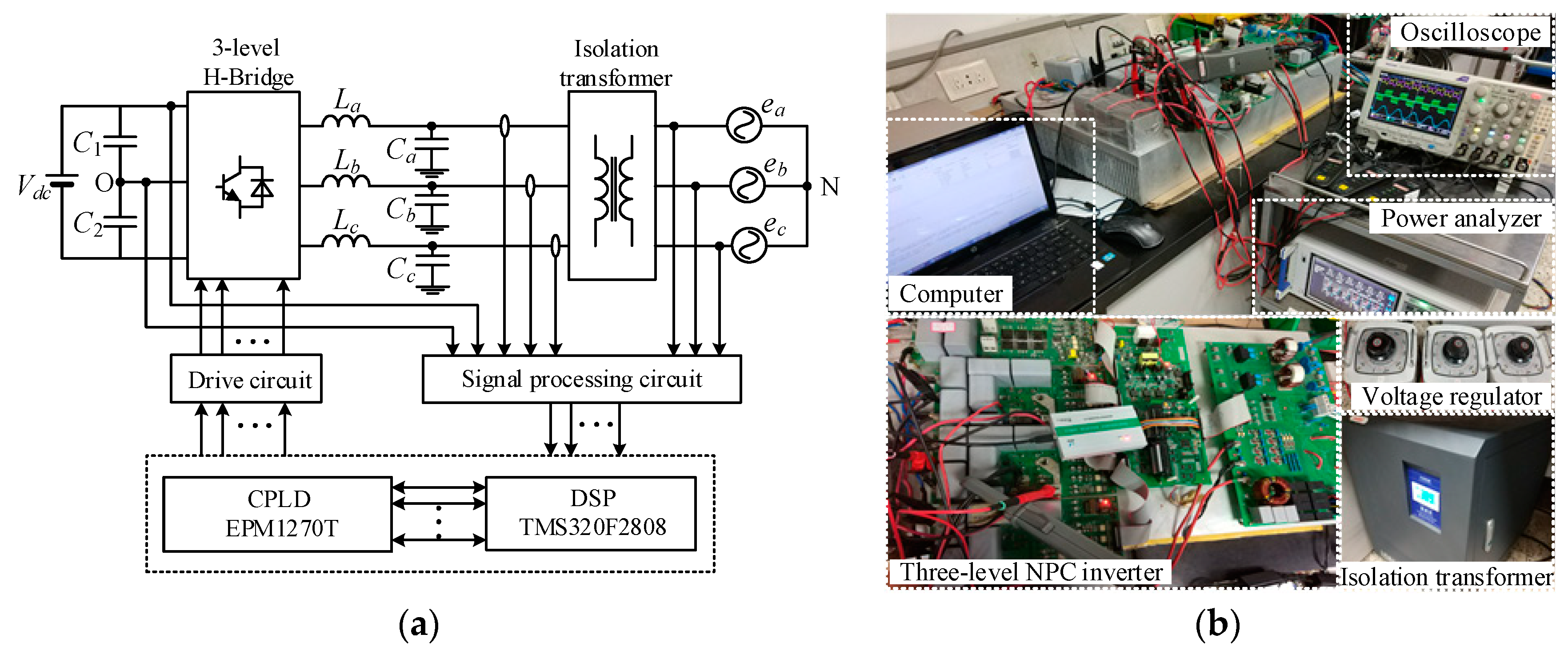
5. Simulation and Experimental Verification

5.1. Simulation Analysis

In order to verify the validity of the proposed DCR-SPWM method, a simulation model of the NPC three-level grid-connected inverter was built using Matlab tools, and the specifications of the simulation model are shown in Table 2.
Figure 9 shows the simulated waveforms of capacitor voltage vc1, vc2, leg voltage vb, grid current ib, and three phase grid voltages ex (x = a, b, c). In Figure 9a,b, the DCR-SPWM method was applied at 0.25 s, where it can be seen that before using the DCR-SPWM method, the capacitor voltage ripple was 20 V at φui = 0, and 30 V at φui = −π/4, respectively. After the DCR-SPWM method was applied, the NP voltage ripple was reduced effectively and the grid current quality improved. In Figure 9c, a parallel resistor was connected to the dc bus capacitor C2 for the NPC three-level grid-connected inverter, resulting in the 40 V dc unbalanced voltage between vc1 and vc2, which made the positive and negative half line cycle of the output leg voltage asymmetric, so as to the grid current. When the DCR-SPWM method was applied, the NP voltage ripple and dc unbalanced voltage could be controlled effectively, and quality of the grid current was improved.

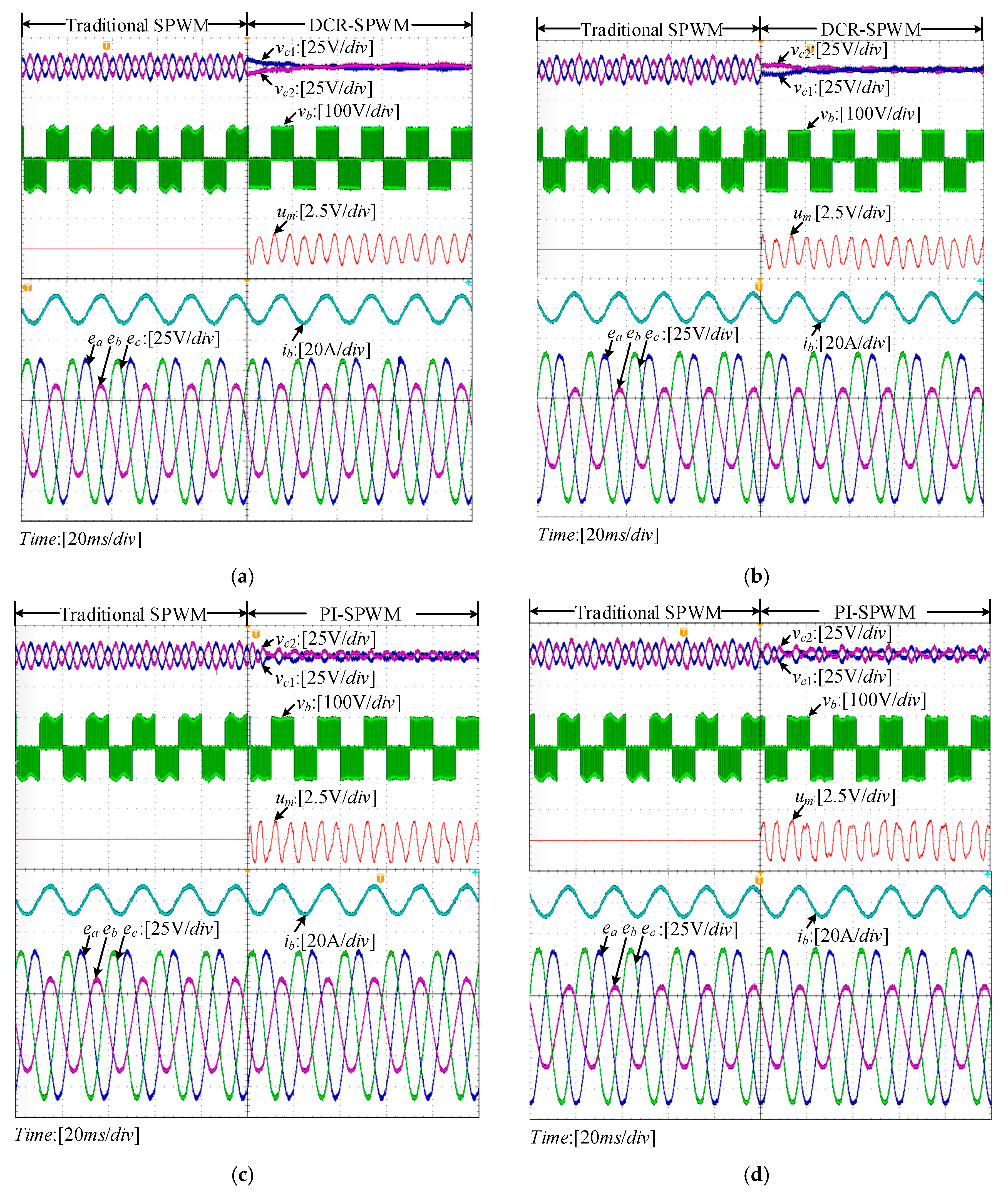
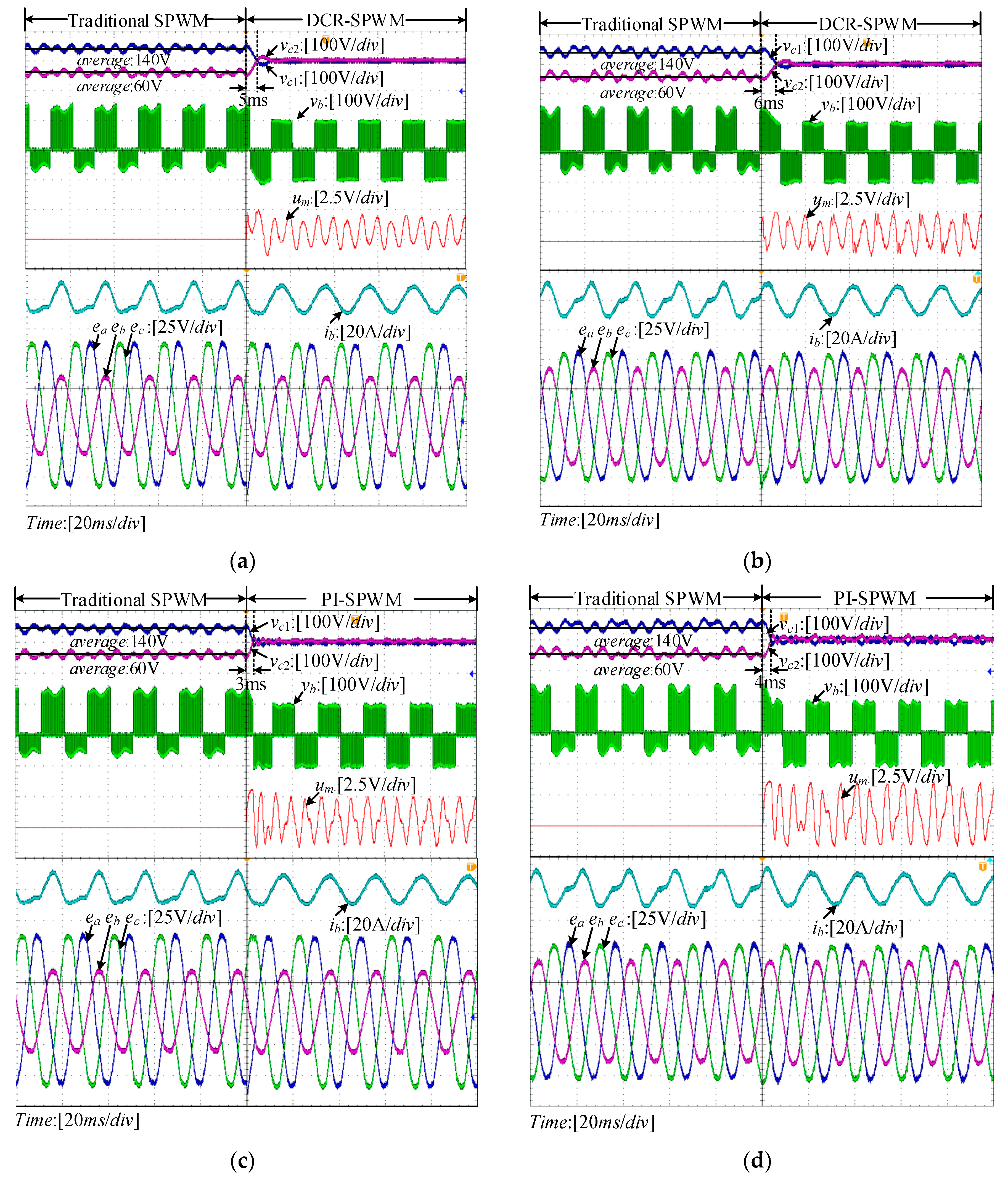
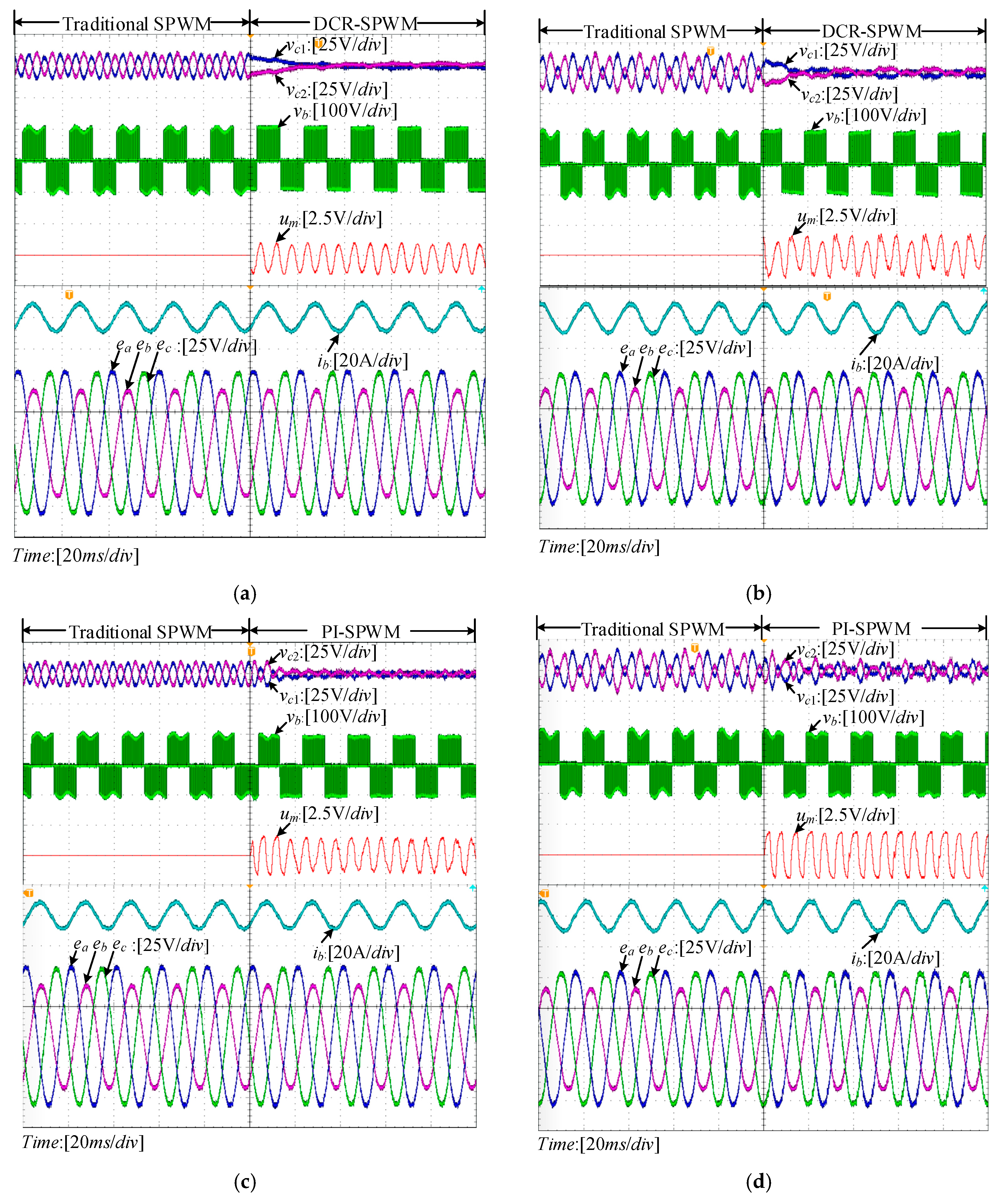
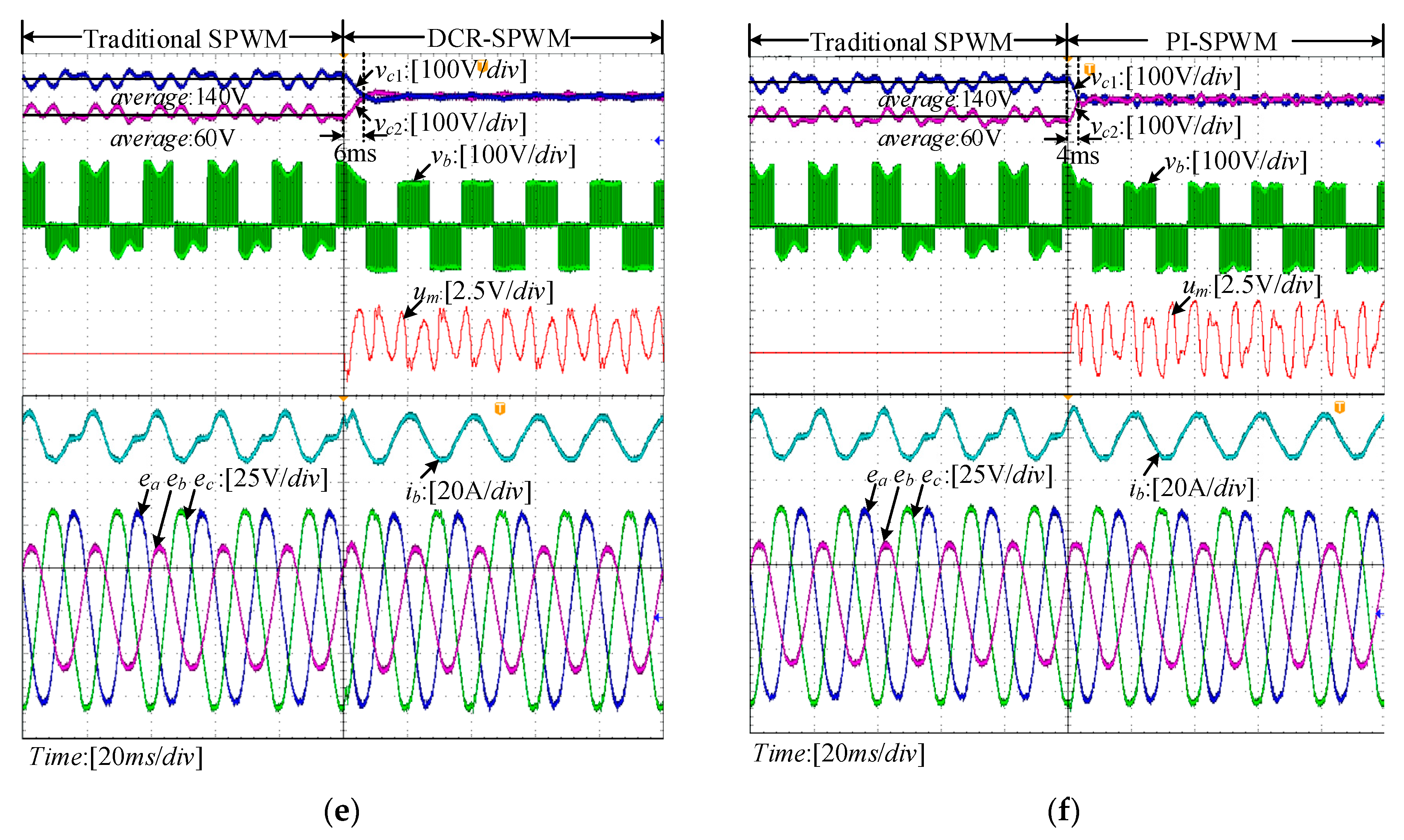
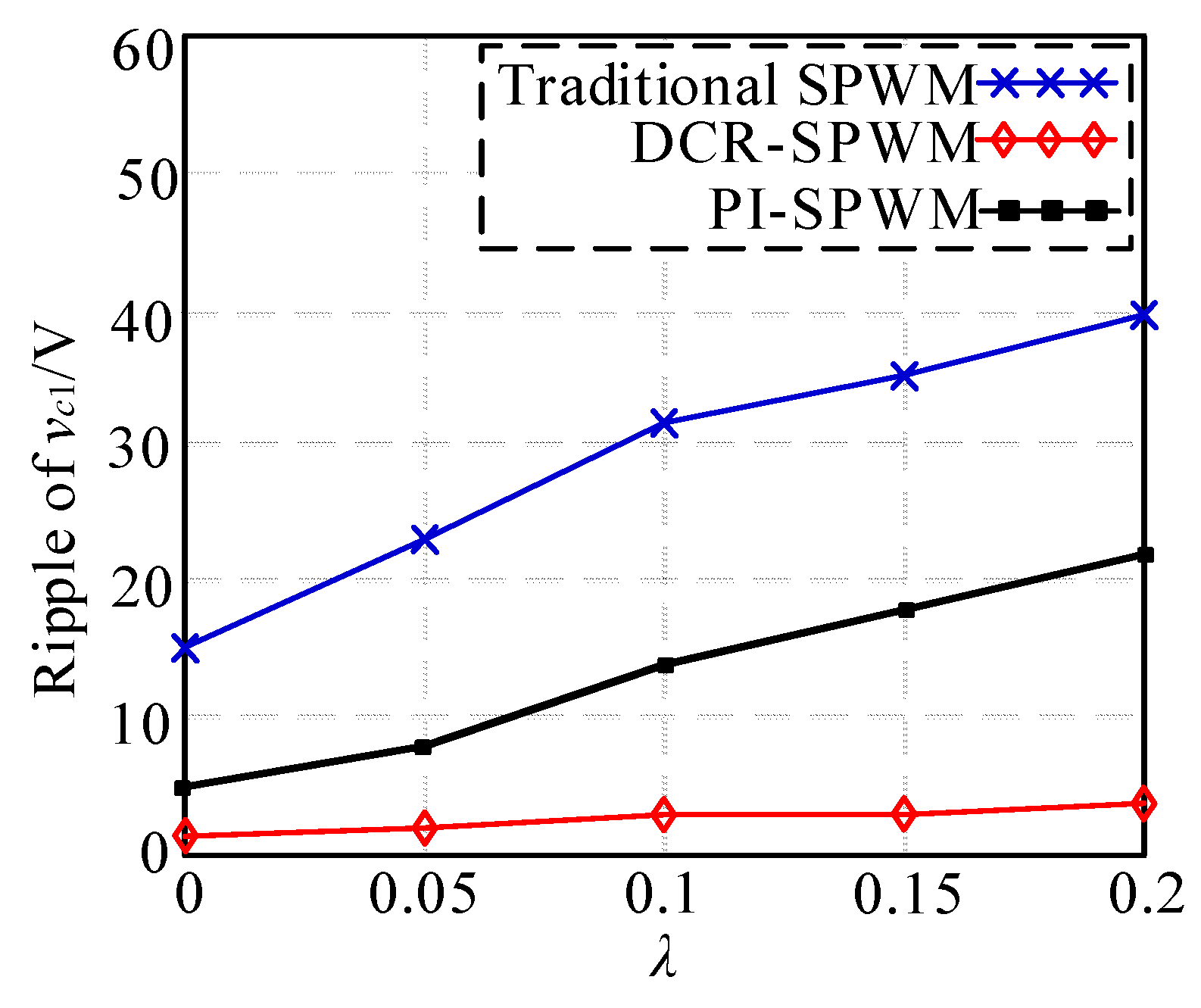
5.2. Experimental Verification

As shown in Figure 10a, the proposed DCR-SPWM method was tested in the experimental platform of an NPC three-level grid-connected inverter based on DSP-CPLD. The experimental platform is shown in Figure 10b where the oscilloscope and power analyzer are Tektronix MDO3000 (Tektronix, Shanghai, China) and HIOKI PW6001 (HIOKI, Nagano, Japan), respectively. The specifications of the experimental prototype are shown in Table 3.
Figure 11 and Figure 12 show the experimental waveforms of vc1, vc2, ib, vb ex (x = a, b, c) and um at different λ and φui conditions, where vb is the leg voltage of phase b and um is zero-sequence voltage that added to the modulation signals, which is added to modulation signals. From Figure 11, it can be seen that when using the traditional SPWM method, the ripple of capacitor voltage vc1 was about 20 V at φui = 0, λ = 0.1 in Figure 11a, and was about 32 V at φui = −π/4, λ = 0.1 in Figure 11b, after the proposed DCR-SPWM method was applied, the ripple of NP voltage was suppressed effectively. In Figure 11c,d, the PI-SPWM method proposed in [14] was applied and it can be seen that the proposed method had better performance in terms of the system steady-state error when compared with the PI-SPWM method.
In Figure 12, before using the DCR-SPWM method, the ripple of vc1 was about 20 V at λ = 0.15, φui = 0 in Figure 12a, and was 24 V at λ = 0.2, φui = 0 in Figure 12b. The NP voltage ripple was very low with the DCR-SPWM method.
When a parallel resistor connected to the dc bus capacitor C2 for the NPC three-level grid-connected inverter, experimental waveforms of vc1, vc2, ib, vb, ex, and um under different conditions are shown in Figure 13, defined that vc1avg and vc2avg were the average voltage of vc1 and vc2, respectively, and before using the DCR-SPWM method, the NP voltage was unbalanced, the voltage difference between vc1avg and vc2avg was about 80 V. In a line cycle, the amplitude of the leg voltage in the positive half cycle was higher than in the negative half cycle, and the quality of the grid current was not beneficial to the grid connections.
When the DCR-SPWM method was applied, the voltage difference between vc1 and vc2 decreased to almost zero, and the ripple of vc1 and vc2 was very low. From Figure 13a,b,e, it can be seen that under different unbalanced grid and output power conditions, the system reached the steady-state rapidly, and the quality of the grid current was improved.
Figure 14 shows the harmonics analysis of the grid current ib under different λ conditions, when φui = −π/4, it can be seen that when the DCR-SPWM method was applied, much low order harmonics were decreased, and the THD value decreased so that the quality of the grid current was beneficial to grid connections.
Figure 15 and Figure 16 show the ripple of vc1 and the THD results of ib at different unbalanced grid conditions with different control methods. It can be seen that with the traditional SPWM method, the ripple of vc1 increased much higher and the THD value was higher than 5% when λ varied from 0 to 0.2 at φui = −π/4, instead, when compared with the PI-SPWM method, the DCR-SPWM method proposed in this paper decreased the ripple of vc1 effectively, and the THD value of grid current was decreased, which was lower than 4%.
According to the experimental and simulation results, under different unbalanced grid and output power conditions, the proposed DCR-SPWM method can suppress the ripple of the NP voltage effectively; when the NP voltage has dc unbalanced voltage, the NP voltage is controlled to be balanced fast, furthermore, this DCR-SPWM method improved the grid current quality and reduced its THD effectively when compared with the PI-SPWM method proposed in [14].

6. Conclusions

In order to solve the NP voltage unbalancing problem for NPC three-level grid-connected inverter under non-ideal grid conditions, the unbalanced form of NP voltage under non-ideal grid conditions was studied, and the DCR-SPWM method under non-ideal grid conditions was proposed. This proposed DCR-SPWM method dynamically calculates the zero-sequence component for modulation signals by region selections, and the theoretical analysis and experiment results showed that the proposed method had a good ability to control the NP voltage balance, and improved the grid current quality effectively.

Author Contributions

J.G.L. conducted the theory analysis and designed the whole project, W.B.H. conducted the experiments, J.D.W. performed the simulation, Z.F.W. and J.D.W. completed the experimental tests. J.D.W. and J.G.L. edited the manuscript.

Acknowledgments

This project was supported by the National Natural Science Foundation of China (51707097), the Fundamental Research Funds for the Central Universities (30917011331), and the Open Research Fund of Jiangsu Collaborative Innovation Center for Smart Distribution Network, Nanjing Institute of Technology (XTCX201708).

Conflicts of Interest

The authors declare no conflict of interest.

References

  1. Wang, Y.; Wang, F. Novel Three-Phase Three-Level-Stacked Neutral Point Clamped Grid-Tied Solar Inverter with a Split Phase Controller. IEEE Trans. Power Electron. 2013, 28, 2856–2866. [Google Scholar] [CrossRef]
  2. Teymour, H.R.; Sutanto, D.; Muttaqi, K.M.; Ciufo, P. Solar PV and Battery Storage Integration Using a New Configuration of a Three-Level NPC Inverter with Advanced Control Strategy. IEEE Trans. Energy Convers. 2014, 29, 354–365. [Google Scholar]
  3. Zhang, Y.; Li, J.; Li, X.; Cao, Y.; Sumner, M.; Xia, C. A Method for the Suppression of Fluctuations in the Neutral-Point Potential of a Three-Level NPC Inverter with a Capacitor-Voltage Loop. IEEE Trans. Power Electron. 2017, 32, 825–836. [Google Scholar] [CrossRef]
  4. Nabae, A.; Takahashi, I.; Akagi, H. A New Neutral-Point-Clamped PWM Inverter. IEEE Trans. Ind. Appl. 1981, IA-17, 518–523. [Google Scholar] [CrossRef]
  5. Rodriguez, J.; Bernet, S.; Steimer, P.K.; Lizama, I.E. A Survey on Neutral-Point-Clamped Inverters. IEEE Trans. Ind. Electron. 2010, 57, 2219–2230. [Google Scholar] [CrossRef]
  6. Zaragoza, J.; Pou, J.; Ceballos, S.; Robles, E.; Ibanez, P.; Villate, J.L. A Comprehensive Study of a Hybrid Modulation Technique for the Neutral-Point-Clamped Converter. IEEE Trans. Ind. Electron. 2009, 56, 294–304. [Google Scholar] [CrossRef]
  7. Choi, U.M.; Lee, H.H.; Lee, K.B. Simple Neutral-Point Voltage Control for Three-Level Inverters Using a Discontinuous Pulse Width Modulation. IEEE Trans. Energy Convers. 2013, 28, 434–443. [Google Scholar] [CrossRef]
  8. Shen, J.; Schröder, S.; Rösner, R.; El-Barbari, S. A Comprehensive Study of Neutral-Point Self-Balancing Effect in Neutral-Point-Clamped Three-Level Inverters. IEEE Trans. Power Electron. 2011, 26, 3084–3095. [Google Scholar] [CrossRef]
  9. Choi, U.M.; Lee, J.S.; Lee, K.B. New modulation strategy to balance the neutral-point voltage for three-level neutral-clamped inverter systems. IEEE Trans. Energy Convers. 2014, 29, 91–100. [Google Scholar] [CrossRef]
  10. Sebaaly, F.; Vahedi, H.; Kanaan, H.Y.; Al-Haddad, K. Novel Current Controller Based on MPC With Fixed Switching Frequency Operation for a Grid-Tied Inverter. IEEE Trans. Ind. Electron. 2018, 65, 6198–6205. [Google Scholar] [CrossRef]
  11. Sebaaly, F.; Vahedi, H.; Kanaan, H.Y.; Moubayed, N.; Al-Haddad, K. Sliding Mode Fixed Frequency Current Controller Design for Grid-Connected NPC Inverter. IEEE Trans. Power Electron. 2016, 4, 1397–1405. [Google Scholar] [CrossRef]
  12. López, I.; Ceballos, S.; Pou, J.; Zaragoza, J.; Andreu, J.; Ibarra, E.; Konstantinou, G. Generalized PWM-based method for multiphase neutral-point-clamped converters with capacitor voltage balance capability. IEEE Trans. Power Electron. 2017, 32, 4878–4890. [Google Scholar] [CrossRef]
  13. Wang, C.; Li, Y. Analysis and calculation of zero-sequence voltage considering neutral-point potential balancing in three-level NPC converters. IEEE Trans. Ind. Electron. 2010, 57, 2262–2271. [Google Scholar] [CrossRef]
  14. Chaturvedi, P.; Jain, S.; Agarwal, P. Carrier-based neutral point potential regulator with reduced switching losses for three-level diode-clamped inverter. IEEE Trans. Ind. Electron. 2014, 61, 613–624. [Google Scholar] [CrossRef]
  15. Maheshwari, R.; Munk-Nielsen, S.; Busquets-Monge, S. Design of neutral-point voltage controller of a three-level NPC inverter with small DC-link capacitors. IEEE Trans. Ind. Electron. 2013, 60, 1861–1871. [Google Scholar] [CrossRef]
  16. Shayestehfard, A.; Mekhilef, S.; Mokhlis, H. IZDPWM-based feedforward controller for grid-connected inverters under unbalanced and distorted conditions. IEEE Trans. Ind. Electron. 2017, 64, 14–21. [Google Scholar] [CrossRef]
  17. Yan, Q.; Wu, X.; Yuan, X.; Geng, Y. An Improved Grid-Voltage Feedforward Strategy for High-Power Three-Phase Grid-Connected Inverters Based on the Simplified Repetitive Predictor. IEEE Trans. Power Electron. 2016, 31, 3880–3897. [Google Scholar] [CrossRef]
  18. Teodorescu, R.; Liserre, M.; Rodríguez, P. Grid Converters for Photovoltaic and Wind Power Systems; John Wiley & Sons: Hoboken, NJ, USA, 2011; pp. 171–172. [Google Scholar]
  19. Ma, K.; Blaabjerg, F. Modulation Methods for Neutral-Point-Clamped Wind Power Converter Achieving Loss and Thermal Redistribution under Low-Voltage Ride-Through. IEEE Trans. Ind. Electron. 2014, 61, 835–845. [Google Scholar] [CrossRef]
  20. Shao, Z.; Zhang, X.; Wang, F.; Cao, R.; Ni, H. Analysis and Control of Neutral-Point Voltage for Transformerless Three-Level PV Inverter in LVRT Operation. IEEE Trans. Power Electron. 2017, 32, 2347–2359. [Google Scholar] [CrossRef]
  21. Vahedi, H.; Labbe, P.A.; Al-Haddad, K. Balancing three-level neutral point clamped inverter DC bus using closed-loop space vector modulation: Real-time implementation and investigation. IET Power Electron. 2016, 9, 2076–2084. [Google Scholar] [CrossRef]
  22. Sebaaly, F.; Vahedi, H.; Kanaan, H.Y.; Moubayed, N.; Al-Haddad, K. Design and Implementation of Space Vector Modulation-Based Sliding Mode Control for Grid-Connected 3L-NPC Inverter. IEEE Trans. Ind. Electron. 2016, 63, 7854–7863. [Google Scholar] [CrossRef]
  23. Jung, K.; Suh, Y. Compensation of neutral point deviation in 3-level NPC converter under unbalanced grid conditions. In Proceedings of the IEEE Applied Power Electronics Conference and Exposition, Long Beach, CA, USA, 20–24 March 2016; pp. 17–24. [Google Scholar]
  24. Jung, K.; Suh, Y. Analysis of neutral point deviation in 3-level NPC converter under unbalanced 3-phase AC grid. In Proceedings of the IEEE Energy Conversion Congress and Exposition, Milwaukee, WI, USA, 18–22 September 2016; pp. 1–8. [Google Scholar]
  25. Von Jouanne, A.; Dai, S.; Zhang, H. A multilevel inverter approach providing DC-link balancing, ride-through enhancement, and common-mode voltage elimination. IEEE Trans. Ind. Electron. 2002, 49, 739–745. [Google Scholar] [CrossRef]
  26. Yaramasu, V.; Wu, B. Predictive control of a three-level boost converter and an NPC inverter for high-power PMSG-based medium voltage wind energy conversion systems. IEEE Trans. Power Electron. 2014, 29, 5308–5322. [Google Scholar] [CrossRef]
  27. Zhang, M.; Hang, L.; Yao, W.; Lu, Z.; Tolbert, L.M. A Novel Strategy for Three-Phase/Switch/Level (Vienna) Rectifier under Severe Unbalanced Grids. IEEE Trans. Ind. Electron. 2013, 60, 4243–4252. [Google Scholar] [CrossRef]
  28. Nejabatkhah, F.; Li, Y.W.; Wu, B. Control Strategies of Three-Phase Distributed Generation Inverters for Grid Unbalanced Voltage Compensation. IEEE Trans. Power Electron. 2016, 31, 5228–5241. [Google Scholar]
  29. Holmes, D.G.; Lipo, T.A. Pulse width Modulation for Power Converters: Principles and Practice; John Wiley & Sons: Hoboken, NJ, USA, 2003; pp. 473–479. [Google Scholar]
Figure 1. Main circuit of the NPC three-level grid-connected inverter.
Energies 11 01331 g001
Figure 2. Single polar SPWM method for NPC three-level inverters.
Energies 11 01331 g002
Figure 3. The waveforms of vc under different grid conditions.
Energies 11 01331 g003
Figure 4. Three phase modulation signals with u0 in different regions under the non-ideal grid condition.
Energies 11 01331 g004
Figure 5. Control principle diagram of the NPC three-level grid-connected inverter.
Energies 11 01331 g005
Figure 6. The flowchart of the DCR unit.
Energies 11 01331 g006
Figure 7. Surfaces of the ripple of vc as the function with φui and λ: (a) Traditional SPWM; (b) DCR-SPWM.
Energies 11 01331 g007
Figure 8. Surfaces of the THD results as the function with φui and λ: (a) Traditional SPWM; (b) DCR-SPWM.
Energies 11 01331 g008
Figure 9. Simulated waveforms of the traditional SPWM and the proposed DCR-SPWM method: (a) φui = 0, vc1avgvc2avg = 0; (b) φui = −π/4, vc1avvc2avg = 0; (c) φui = 0, vc1avgvc2avg = 40 V.
Energies 11 01331 g009
Figure 10. The schematic diagram and experimental photograph of the system: (a) Schematic diagram of the system; (b) Experimental photograph of the system.
Energies 11 01331 g010
Figure 11. Experimental waveforms under different φui conditions: (a) DCR-SPWM φui = 0, λ = 0.1, vc1avvc2avg = 0; (b) DCR-SPWM φui = −π/4, λ = 0.1, vc1avgvc2avg = 0; (c) PI-SPWM φui = 0, λ = 0.1, vc1avgvc2avg = 0; (d) PI-SPWM φui = −π/4, λ = 0.1, vc1avgvc2avg = 0.
Energies 11 01331 g011
Figure 12. Experimental waveforms under different λ conditions: (a) DCR-SPWM φui = 0, λ = 0.15, vc1avgvc2avg = 0; (b) DCR-SPWM φui = 0, λ = 0.2, vc1avgvc2avg = 0; (c) PI-SPWM φui = 0, λ = 0.15, vc1avgvc2avg = 0; (d) PI-SPWM φui = 0, λ = 0.2, vc1avgvc2avg = 0.
Energies 11 01331 g012
Figure 13. Experimental waveforms under dc unbalanced NP voltage conditions: (a) DCR-SPWM φui = 0, λ = 0.2, vc1avgvc2avg = 80 V; (b) DCR-SPWM φui = −π/4, λ = 0.1, vc1avgvc2avg = 80 V; (c) PI-SPWM φui = 0, λ = 0.2, vc1avgvc2avg = 80 V; (d) PI-SPWM φui = −π/4, λ = 0.1, vc1avgvc2avg = 80 V; (e) DCR-SPWM φui = −π/4, λ = 0.15, vc1avgvc2avg = 80 V; (f) PI-SPWM φui = −π/4, λ = 0.15, vc1avgvc2avg = 80 V.
Energies 11 01331 g013aEnergies 11 01331 g013b
Figure 14. Harmonics distribution of ib: (a) λ = 0.1; (b) λ = 0.15; (c) λ = 0.2.
Energies 11 01331 g014
Figure 15. Measured NP voltage ripple.
Energies 11 01331 g015
Figure 16. Measured THD.
Energies 11 01331 g016
Table 1. Expressions of Ai, Bi and Ci.
CoefficientExpressions
Aa I m p 2 E m p V d c [ 3 λ 2 cos ( φ u i 2 φ u n ) + 3 λ cos ( φ u i φ u n φ u p ) + 3 cos ( φ u i 2 φ u p ) ]
Ba I m p 2 E m p V d c [ 3 λ 2 sin ( φ u i 2 φ u n ) 3 λ sin ( φ u i φ u n φ u p ) 3 sin ( φ u i 2 φ u p ) ]
Ca I m p 2 E m p V d c [ 3 2 ( λ 2 + 1 ) sin ( φ u i ) 2 3 λ sin ( φ u i ) cos ( φ u n φ u p ) ]
Ab I m p 2 E m p V d c [ 3 λ 2 sin ( φ u i 2 φ u n + π 6 ) + 3 λ cos ( φ u i φ u n φ u p ) + 3 sin ( φ u i 2 φ u p π 6 ) ]
Bb I m p 2 E m p V d c [ 3 λ 2 sin ( φ u i 2 φ u n π 3 ) 3 λ sin ( φ u i φ u n φ u p ) + 3 sin ( φ u i 2 φ u p + π 3 ) ]
Cb I m p 2 E m p V d c [ 3 2 ( λ 2 + 1 ) sin ( φ u i ) + 2 3 λ sin ( φ u i ) cos ( φ u n φ u p + π 3 ) ]
Ac I m p 2 E m p V d c [ 3 λ 2 sin ( φ u i 2 φ u n π 6 ) + 3 λ cos ( φ u i φ u n φ u p ) 3 sin ( φ u i 2 φ u p + π 6 ) ]
Bc I m p 2 E m p V d c [ 3 λ 2 sin ( φ u i 2 φ u n + π 3 ) 3 λ sin ( φ u i φ u n φ u p ) + 3 sin ( φ u i 2 φ u p π 3 ) ]
Cc I m p 2 E m p V d c [ 3 2 ( λ 2 + 1 ) sin ( φ u i ) + 2 3 λ sin ( φ u i ) cos ( φ u n φ u p π 3 ) ]
Table 2. Specifications of the prototype for simulation.
Specifications of the Prototype
DC bus voltageVdc = 200 V
DC bus capacitorsC1 = C2 = 150 μF
Switching frequencyfs = 16 kHz
Apparent powerS = 600 VA
The amplitude of grid voltagesEma = 55 V, Emb = 40 V, Emc = 55 V
Output phase filterL: 1.5 mH, C: 15 μF
Table 3. Specifications of the experimental prototype.
The Specifications of the Experimental Prototype
DC bus voltageVdc = 200 V
DC bus capacitorsC1 = C2 = 150 μF
Switching frequencyfs = 16 kHz
Apparent powerS = 600 VA
Digital Process UnitDSP: TMS320F2808, CPLD: EPM1270T
Power switches moduleIGBT FZ06NPA070FP
Output phase filterL: 1.5 mH, C: 15 μF

