Abstract
The battery management system (BMS) is the key development for energy storage systems, and battery balancing is an important subsystem of the BMS. However, with rapid development of supercapacitors, future energy storage cells are not constrained by one type, while different types of cells may form a source package (SP). Furthermore, the introduction of second-life batteries from retired electric vehicles promotes the demand of effective balancing systems for SPs with hybrid cells, as well as the requirement that balancing should be extended to any preset ratio rather than 1:1. This paper proposes a novel tapped inductor balancing circuit that allows any ratio of voltage balancing for hybrid energy storage cells. The analysis of the circuit, simulation and experiment results are presented to demonstrate its effectiveness in handling hybrid source balancing.
1. Introduction
Energy storage based on electrical means is an important development because several green energy systems such as electric mobility, power distribution and renewable energy sources need a vast amount of energy storage to ensure stable operation. Battery and supercapacitor (SC) are two prominent types, because they are already widely used and have proved to be cost effective. Circuit technology has been developed to prevent cell imbalance. Cell balancing is important because it avoids the overcharge and undercharge of cells to ensure safety [1,2].
In recent years, the campaign to solve out the recycling of a large number of aged batteries from retired electric vehicles has received increasing attention. It is known that retired batteries from electric vehicles still have 70 to 80% of state of health (SoH), which remains very useful for energy storage in stationery applications where the energy density is not in high demand; for example, the energy storage for peak-and-trough compensation from power plant, interruptible power supply and renewable energy storage systems.
Usually, single cells of battery/SC are packed into a source package. The cell voltage among different cells should be kept equal all the time to ensure that each cell is under the same operational condition. As not all the cells are identical, the cell balancing is therefore introduced and researched [3,4,5,6]. One of the most common types is to use classical switched-mode power converter buck-boost that is illustrated in Figure 1a. An inductor is used to transfer the excess charge from one cell to another using the buck-boost power conversion. The concept has been extended to couple an inductor to assist the balancing [7]. Figure 1b,c are two popular cell balancings that have been reported extensively. Figure 1b is based on switched-capacitor [8,9]. The method is similar to [10] where all cells are switched to common energy storage to equalize the voltage. Figure 1c is transformer-based and uses windings to balance each cell. [11,12] use a bi-directional switch with two anti-series MOSFETs to connect each cell to its balancing winding. Recently, the wireless power transfer approach for balancing is reported in [13] that uses an air-gapped transformer to conduct the wireless power transition. Recent research mainly focuses on the equal voltage balancing, i.e., mainly balancing cells of same type with voltage ratio of 1:1.
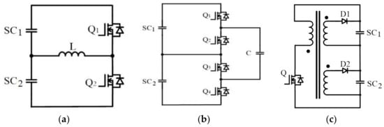
Figure 1.
Basic topology of cell-balancing. (a) Buck-boost converter; (b) Capacitor balancing; (c) Transformer balancing.
Table 1 shows an example of different voltages of Li-ion cells [14,15]. Currently, the source package is mainly composed of standardized battery cells with the same chemical combination and initial voltage.

Table 1.
Example of cell voltage for Li-ion batteries.
The use of second life battery is getting popular [16,17,18]. Extensive research has been reported. Different combinations of cells may be connected in a battery pack or module [19,20]. The cells usually have different states of health, cell voltage and capacity. Also, there could also be a combination of battery and other energy storage devices such as SCs with different voltage levels. Even SC cells may have different voltages as well. Furthermore, in some circumstances, balancing among different source packages should be achieved. Therefore, an alternative balancing circuit with any voltage conversion is needed for universal application.
In this paper, a novel balancing circuit is proposed using tapped inductor techniques. Different from buck-boost converter and switched-capacitor, tapped inductor has advantages in step-free adjustment and is suitable for balancing hybrid source packages composed of SCs, batteries and aged batteries. Other converters such as H-bridge or resonant converter have been considered for suitable circuit for cell balancing, but will complicate the overall circuitry with added advantage of soft-cell balancing [21,22]. The rest of this paper is arranged as follows: Section 2 describes the basic circuit of the tapped inductor. Section 3 presents the circuitry of the tapped inductor balancing circuit. The modeling of the circuit is obtained in Section 4. The simulation and experimental results will be presented in the Section 5 and Section 6, respectively.
2. Tapped Inductor Basic Circuit
2.1. Conventional Buck-Boost Balancing
The conventional switched mode power conversion, buck-boost for example, can be used by adjusting different duty ratios of and to provide balancing for and in Figure 1. This is expressed as follows:
where and are the voltage of and , respectively. and is the duty ratio of and respectively. It is noted that
When the voltage ratios of and are different in more than 2, the efficiency of the voltage conversion between and is low [23,24]. By using transformer concept or the isolated power converter such as forward converter or flyback converter, the efficiency of voltage conversion can be much higher when its transformer’s turns ratio is much larger. The concept has been developed widely and realized by tapped inductor converter [25].
2.2. The Tapped Inductor Basic Theory
Figure 2 shows a generalized circuit for three basic topologies in switched-mode power converter (SPMC). The transistor is connected to the tapped inductor L with the number of turns being m and the diode is connected to the tapped inductor with the number of turns being n. Since the magnetomotive force (mmf) is conservative for the tapped inductor, therefore, the voltage conversion ratio between and can be derived as follows.
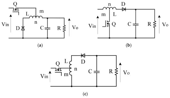
Figure 2.
General topology of tapped inductor for three basic SMPC topologies. (a) Buck converter; (b) Boost converter; (c) Buck-boost converter.
To illustrate the voltage conversion for tapped inductor, the mmf values of Mon and Moff during the period when Q is turned on are:
where Lm and Ln are the inductance of the inductors with m and n turns, respectively. VLm and VLn are the voltage across Lm and Ln, respectively. D1 and D2 are the turn-on duty ratio of transistor and diode respectively.
(3) and (4) can be reduced to
and
For the application to the three basic topologies, the voltage conversion ratio k is then:
Buck converter:
Boost converter:
Buck-boost converter:
where
3. The Tapped Inductor Balancing
3.1. Basic Cell Equalization
Figure 1a and Figure 2c can be combined into a tapped inductor balancing that makes use of the large voltage conversion for input and output. The diode is changed into a MOSFET and therefore a bi-directional power flow can be obtained that allows the energy balancing between two different source packages. Figure 3a shows the topology that is also a buck-boost version. m and n are the number of turns obtained from the tapped inductor when the transistors Q1 and Q2 are on respectively.
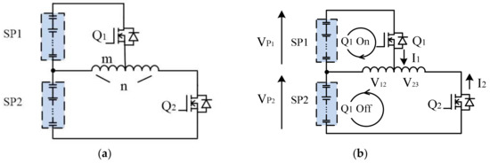
Figure 3.
Tapped inductor balancing circuit. (a) Basic circuit; (b) Current flow during on and off states of transistor.
The circuit analysis is similar to the conventional analysis of an SMPC. The voltage balancing equation then becomes:
where VP1 is the voltage of SP1 and VP2 is the voltage of SP2.
In particular cases, if D1 = 0.5, it is reduced to a transformer turns ratio to voltage ratio relationship:
In this case, each transistor is turned on for half a cycle in a complementary manner. The efficiency of such tapped inductor power conversion is high and using coupled-inductor’s turns ratio, any voltage conversion can be obtained, that is, balancing of battery or SC hybrid source packages under any voltage ratios can be achieved.
3.2. Generalized Cell Equalization
The above circuit can be extended to a string of i packages as shown in Figure 4. The xth tapped inductor Lx, coupled with source package SPx, has a tapping and the turns ratio is where x varies from 1 to i − 1. The operation process of the proposed balancing system is divided into on state and off state with different switch signals Vg_Q and Vg_S in one cycle T as demonstrated in Figure 5. The balancing is self-adaptive and automatically converges to equilibrium. The current between the source packages could be close to zero when the voltages of the source packages are equal after balancing progress and the loss is small. The detailed operation principles of the two states are shown in Section 4.
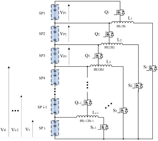
Figure 4.
Generalized tapped inductor cell equalization circuit.
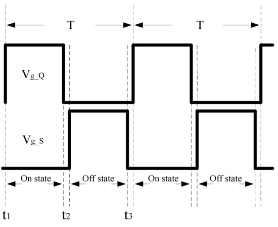
Figure 5.
Control signal of the switches.
The equalization equation for SPx is:
where is the voltage of the SPx. Vx is the total voltage from SPi to SPx. Dx is the duty ratio of Qx and Sx.
When all the SP voltages are balanced, D = 0.5 is adopted to maintain the equalization of the cell voltage. Based on (14), the voltage ratio could be further edited as:
4. Modeling of Tapped Inductor Voltage Equalizer
4.1. Operation Principle and Average Current Analysis
During the progress of charging/discharging in one cycle, the charge is transferred between SP1 and SP2. The transistor is turned on and off and the circuit parameters vary accordingly. The equivalent model of the balancing circuit is shown in Figure 6. The equivalent series resistance and on-state voltage for the diode are included to assist the modeling.
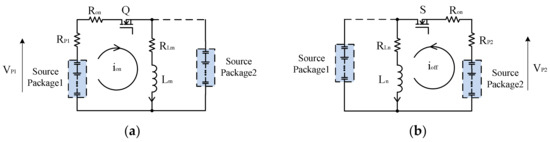
Figure 6.
Equivalent Model of the balance circuit. (a) on-state; (b) off-state.
Based on the relationship of (3) and (4), the mmf between SP1 and SP2 are
where .
According to KVL, (16) could be further expressed as
where , . is the on-resistance of the switch; , are the equivalent series resistance (ESR) of the inductor in m and n turns respectively, such that ; and are the ESR of the source packages; and are instantaneous current across L when the switch is on and off.
and are the average current across L when the switch is on and off, respectively, so that .
Assume when and , could be obtained from (17) as:
The average current Iavg of SP1 is
4.2. Energy Conversion Loss Analysis
During balancing progress, all the energy transfers between source packages, from the higher voltage source to lower voltage source. In the end of the progress, each of the SP voltage is under the ratio shown in (15).
The variation of is
where is the current difference during the on state.
The energy discharged Edch from SP1 throughout one cycle is:
The variation of is
where is the current difference during the off state.
The energy charged Ech to the SP2 is
The energy transferred in the tapped inductors is . The variation of and are presented below
By equaling (24) to (25), the energy conversion loss is
where , .
As shown in (26), the initial voltage of SPs, voltage ratio, frequency, inductance, duty ratio and ESR will affect the energy conversion loss.
5. Simulation Study
The above balancing process has been simulated by PSIM software to study the performance of the circuit. Assume that the source packages are composed of the SCs with the same capacitance 350F. For the tapped inductor, L = 400 µH is simulated while f = 30 kHz and D = 0.5 of the control signals are used to operate the circuit. The voltage ratio of are simulated by 1:2:3, 1:2:4, 1:3:9 while according to (15), the turn ratios are 1:5, 1:6, 1:12 for L1 and 2:3, 1:2, 1:3 for L2.
Table 2 indicates simulation results of the waveforms for voltage balance and the average current under the schematic in Figure 7 with different voltage ratios. Because of the preset voltage ratio and initial voltages, SP1 is discharged and SP2 and SP3 are charged for voltage ratio of 1:2:3; the SP1 and SP2 are discharged and SP3 is charged for voltage ratio of 1:2:4 and 1:3:9. The voltage of each source package varies under the voltage ratio in the equalization process, and it is apparent that the balancing phenomenon conforms to the principles in (15). The variation of average current and energy loss in the simulations are consistent with the principles in (19) and (26).
Table 2.
Simulation results of the Tapped Inductor voltage equalizer.
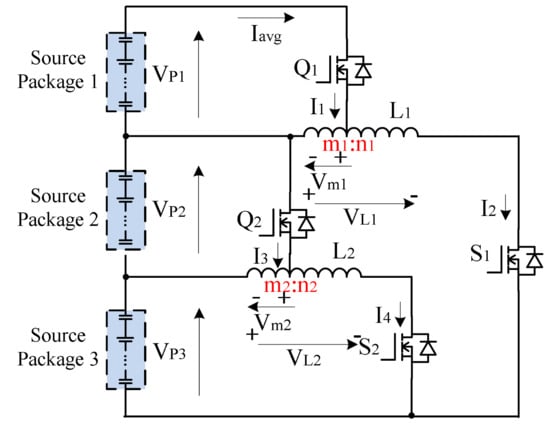
Figure 7.
Topologies for simulation.
6. Experimental Results
To verify the validity of mathematical derivation and software simulation, a 1:2:3 voltage ratio tapped inductor balancing circuit is built in laboratory and all the SPs are tested in the same ambient temperature (20 °C). The inductors are made in the laboratory with 1:5 and 2:3 turns ratio. All the transistors are continuously pulsed as the method in Section 3. Although the control method could be used to trigger the unbalanced cells to accelerate the balancing speed, because the unbalancing speed is slow as compared with the speed of balancing of proposed balancing circuit, therefore the present control is to use continuous triggering to all transistors and it reduces the control complication and the system is therefore absolutely stable. The balancing current will be reduced to zero when the equalization is achieved. Topology of the equalizer is shown in Figure 7 and the list of components is recorded in Table 3. SP1, SP2, SP3 are formed by one SC, two SCs and three SCs connected in series and the list of components is recorded in Table 3. The size of the components in the control circuit of this balancing circuit is much smaller than the SPs because the balancing current is only a very small percentage of the main current of the SP. The circuit is suitable for practical use.
Table 3.
Parameters in the experiment.
The source packages, SP1, SP2 and SP3 are charged to the initial voltages of around 2.01 V, 4.22 V and 7.18 V, respectively. The balancing process is started by enabling the gating signals of the equalizer prototype. The voltage balancing process of the experiment is shown in Figure 8. After the voltage balancing progress, all , and are balanced to the same voltage magnitude, which coincides with the results of theoretical analysis. Besides, the average current and energy loss are close to the principles in (16) and (23).
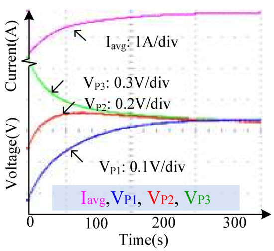
Figure 8.
The balancing waveforms and average current waveform from the experiment in the laboratory. (CH1: Iavg is average discharge current; CH2: VP1 is voltage of source package1; CH3: VP2 is voltage of source package2; CH4: VP3 is voltage of source package3).
Figure 9 and Figure 10 depict the voltage and current variation of tapped inductor L1 and tapped inductor L2 during 30 kHz frequency. The ripple of currents I1, I2, I3 and I4 is small. The experiment results demonstrate that the variation of all voltage and current conforms to the charging/discharging principles in the balance progress.
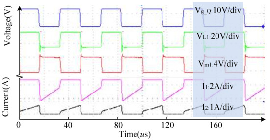
Figure 9.
The voltage and current waveforms of tapped inductor L1 during the balancing progress. (CH1. Vg_Q is gate signal of switches Q1 and Q2; CH2: VL1 is voltage between the whole turns of the L1; CH3: Vm1 is voltage between the left side of the L1; CH4: I1 is current flows across Q1; CH5: I2 is current flows across S1).
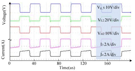
Figure 10.
The voltage and current waveforms of tapped inductor L2 during the balancing progress. (CH1: Vg_S is gate signal of switches S1 and S2; CH2: VL2 is voltage between the whole turns of the L2; CH3: Vm2 is voltage between the left side of the L2; CH4: I3 is current flows across Q2; CH5: I4 is current flows across S2).
Retired batteries from electric vehicles have different voltage characteristics. For convenience of experiment, this paper took SC combination as the energy sources. However, as the tapped inductor balancing circuit proposed in this paper can be applied with any preset voltage ratio, the integration of second life batteries will not weaken the effectiveness of this non-equal voltage balancing technique. In practical design with PCB implementation, it is possible to keep the size of the balancing system at much less than one-tenth of the size of the whole packages with the proposed circuit topology. In theory, the inductor size can be further reduced by increasing the switching frequency. Therefore, the proposed method is a practical cell balancing solution for managing hybrid source packages with difference voltage ratios.
7. Conclusions
A new concept of source package equalization has been reported using a tapped inductor method. The method is derived from conventional tapped inductor converter. The advantage of the method is that it can allow cell balancing of any ratio with high efficiency. The proposed concept can be extended to several hybrid cells connected. Simulation and experimental results have been presented to demonstrate the effectiveness of this circuit. The proposed scheme is especially useful when second-life battery and other new types of energy are universally applied to energy storage systems, peak power compensation and even uninterruptible power supply.
Author Contributions
Xiaolin Wang proposed the theoretical models and conduct the experiment, and Ka Wai Eric Cheng and Yat Chi Fong provided guidance and key suggestions.
Acknowledgments
The authors gratefully acknowledge the support of China Dynamic Electric Vehicle Ltd., the Research committee of the Hong Kong Polytechnic University and Innovation and Technology Fund under the project references: H-ZDAN and GHP/057/14AP.
Conflicts of Interest
The authors declare no conflict of interest.
References
- Gao, Z.C.; Chin, C.S.; Chiew, J.; Jia, J.B.; Zhang, C.Z. Design and Implementation of Smart Lithium-ion Battery System with Real-time Fault Diagnosis Capability for Electric Vehicles. Energies 2017, 10, 1503. [Google Scholar] [CrossRef]
- Gao, Z.C.; Chin, C.S.; Woo, W.L.; Jia, J.B. Integrated Equivalent Circuit and Thermal Model for Simulation of Temperature-Dependent LiFePO4 Battery in Actual Embedded Application. Energies 2017, 10, 85. [Google Scholar] [CrossRef]
- Cheng, K.W.E.; Divakar, B.P.; Wu, H.; Ding, K.; Ho, H.F. Battery-Management System (BMS) and SOC Development for Electrical Vehicles. IEEE Trans. Veh. Technol. 2011, 60, 76–88. [Google Scholar] [CrossRef]
- Peng, X.; He, X.; Han, P.; Guo, A.; Shu, Z.; Gao, S. Smooth switching technique for voltage balance management based on three-level neutral point clamped cascaded rectifier. Energies 2016, 9, 803. [Google Scholar] [CrossRef]
- Park, S.H.; Park, K.B.; Kim, S.H.; Moon, G.W.; Youn, M.J. Single-Magnetic Cell-to-Cell Charge Equalization Converter With Reduced Number of Transformer Windings. IEEE Trans. Power Electron. 2012, 27, 2900–2911. [Google Scholar] [CrossRef]
- Gao, Z.C.; Chin, C.S.; Toh, W.D.; Chiew, J.; Jia, J. State-of-Charge Estimation and Active Cell Pack Balancing Design of Lithium Battery Power System for Smart Electric Vehicle. J. Adv. Transp. 2017. [Google Scholar] [CrossRef]
- Daowd, M.; Antoine, M.; Omar, N.; Bossche, P.V.D.; Mierlo, J.V. Single switched capacitor battery balancing system enhancements. Energies 2013, 6, 2149–2174. [Google Scholar] [CrossRef]
- Law, K.K.; Cheng, K.W.E. Examination of the frequency modulation and lifting techniques for the generalized power factor correction switched-capacitor resonant converter. Int. J. Circuit Theory Appl. 2008, 7, 839–855. [Google Scholar] [CrossRef]
- Ye, Y.; Cheng, K.W.E.; Fong, Y.C. Topology, Modeling, and Design of Switched-Capacitor-Based Cell Balancing Systems and Their Balancing Exploration. IEEE Trans. Power Electron. 2017, 32, 4444–4454. [Google Scholar] [CrossRef]
- Feng, F.; Lu, R.; Zhu, C. Equalisation strategy for serially connected LiFePO4 battery cells. IET Electr. Syst. Transp. 2016, 6, 246–252. [Google Scholar]
- Lambert, S.M.; Pickert, V.; Atkinson, D.J.; Zhan, H. Transformer-Based Equalization Circuit Applied to n-Number of High Capacitance Cells. IEEE Trans. Power Electron. 2016, 31, 1334–1343. [Google Scholar] [CrossRef]
- Chen, Y.; Liu, X.; Cui, Y.; Zou, J.; Yang, S. A MultiWinding Transformer Cell-to-Cell Active Equalization Method for Lithium-Ion Batteries With Reduced Number of Driving Circuits. IEEE Trans. Power Electron. 2016, 31, 4916–4929. [Google Scholar]
- Liu, M.; Fu, M.; Wang, Y.; Ma, C. Battery Cell Equalization via Megahertz Multiple-Receiver Wireless Power Transfer. IEEE Trans. Power Electron. 2018, 33, 4135–4144. [Google Scholar] [CrossRef]
- Cheng, K.W.E. Review of battery management systems for electric vehicles. In Energy Systems for Electric and Hybrid Vehicles; IET: London, UK, 2016; ISBN 978-1-78561-008-0. [Google Scholar]
- Xiong, R.; He, H.; Sun, F.; Zhao, K. Online estimation of peak power capability of Li-ion batteries in electric vehicles by a hardware-in-loop approach. Energies 2012, 5, 1455–1469. [Google Scholar] [CrossRef]
- Choe, J.M.; Choe, G.H.; Lai, J.S. System for load levelling control and operation of an energy storage system. IET Power Electron. 2017, 10, 739–745. [Google Scholar] [CrossRef]
- Casals, L.C.; Garca, B.A. Communications concerns for reused electric vehicle batteries in smart grids. IEEE Commun. Mag. 2016, 54, 120–125. [Google Scholar] [CrossRef]
- Monem, M.A.; Hegazy, O.; Omar, N.; Trad, K.; Breucker, S.D.; Bossche, P.V.D. Design and analysis of generic energy management strategy for controlling second-life battery systems in stationary applications. Energies 2016, 9, 889. [Google Scholar] [CrossRef]
- Mukherjee, N.; Strickland, D. Control of Second-Life Hybrid Battery Energy Storage System Based on Modular Boost-Multilevel Buck Converter. IEEE Trans. Ind. Electron. 2015, 62, 1034–1046. [Google Scholar] [CrossRef]
- Mukherjee, N.; Strickland, D. Analysis and Comparative Study of Different Converter Modes in Modular Second-Life Hybrid Battery Energy Storage Systems. IEEE J. Emerg. Sel. Top. Power Electron. 2016, 4, 547–563. [Google Scholar] [CrossRef]
- Chan, H.L.; Cheng, K.W.E.; Sutanto, D. Bidirectional phase-shifted DC-DC converter. IEE Electron. Lett. 1999, 35, 523–524. [Google Scholar] [CrossRef]
- Cheng, K.W.E.; Evans, P.D. Parallel-mode extended-period quasiresonant convertor. IEE Proc. B 1991, 138, 243–251. [Google Scholar] [CrossRef]
- Shi, Z.H.; Cheng, K.W.E.; Ho, S.L. Static performance and parasitic analysis of tapped-inductor converters. IET Power Electron. 2014, 7, 366–375. [Google Scholar] [CrossRef]
- Li, S.; Cheng, K.W.E.; Ye, Y.; Shi, Z. Wide input and wide output topology analysis for tapped-inductor converters with consideration of parasitic elements. IET Power Electron. 2016, 9, 1952–1961. [Google Scholar] [CrossRef]
- Grant, D.A.; Darroman, Y. Watkins-Johnson converter completes tapped inductor converter matrix. Electron. Lett. 2003, 39, 271–272. [Google Scholar] [CrossRef]


© 2018 by the authors. Licensee MDPI, Basel, Switzerland. This article is an open access article distributed under the terms and conditions of the Creative Commons Attribution (CC BY) license (http://creativecommons.org/licenses/by/4.0/).