1. Introduction
In micro-grid applications, line frequency transformers (LFTs), in correspondence with mechanical breakers, are usually employed to interconnect a micro-grid with the main grid. LFTs work at the line frequency to perform AC to AC power conversion. However, the deep penetration of renewable energy causes negative effects to the distribution line, e.g., voltage fluctuation, frequency variation, etc. The undesired fluctuations may be transferred to the downstream or upstream utilities via LFTs and cause excessive operation of mechanical voltage stabilizers [
1].
In order to improve the power quality, reliability and stability, there are some possible solutions, such as adopting Flexible Alternating Current Transmission System (FACTS) devices [
2] to process the fluctuations at the point of common coupling or using Solid-State-Transformers (SSTs) [
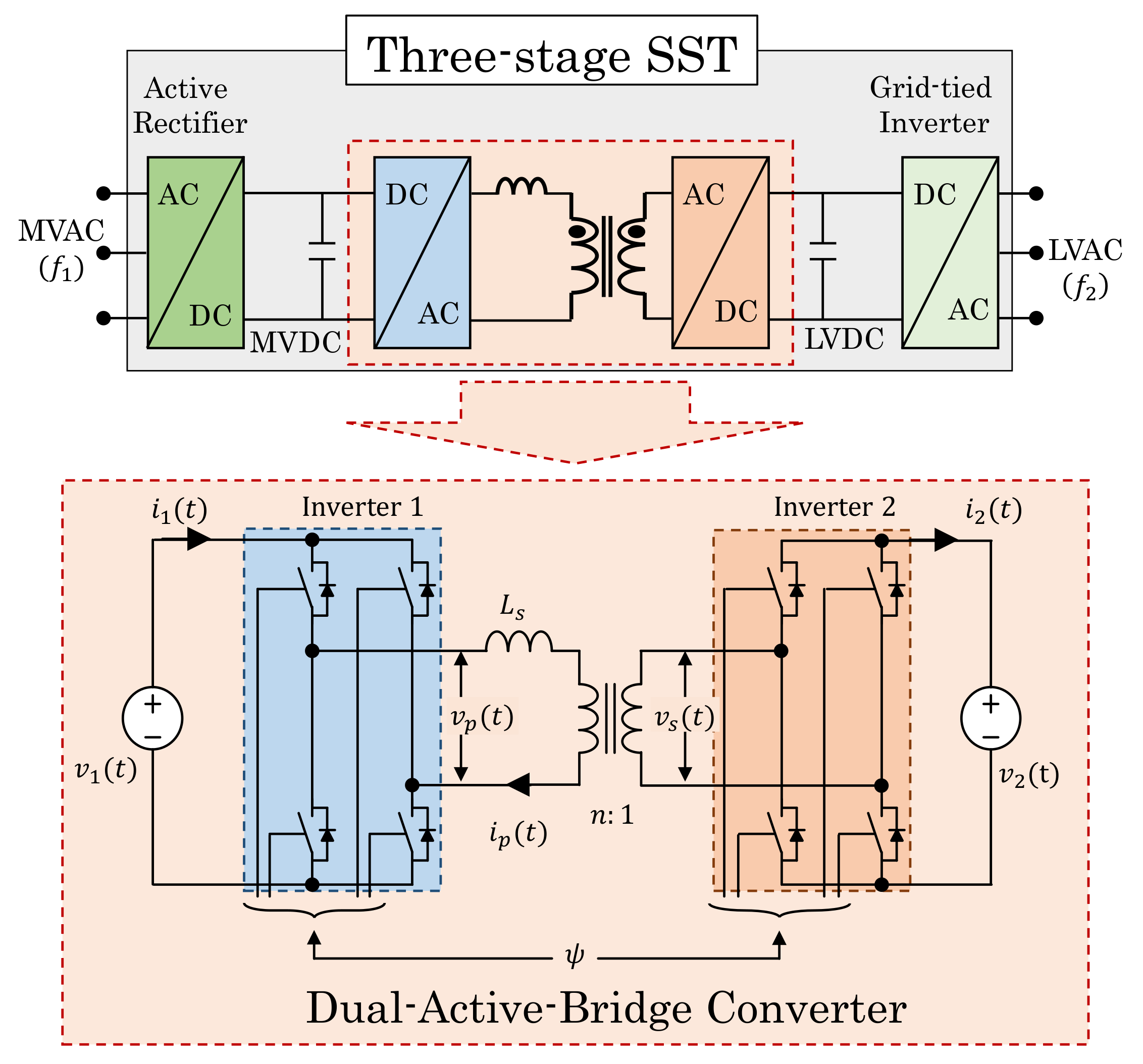
3] instead of LFTs. Among those, the SST, which is depicted in
Figure 1, appears to be a promising device to resolve the aforementioned problems.
An SST consists of three main parts: an active rectifier, a bidirectional Dual-Active-Bridge (DAB) DC/DC converter and an inverter. Compared to LFTs, SSTs do not only allow galvanic isolation and bidirectional power transmission but can also be used for all kinds of electric power conversion, not only AC–AC conversion. Furthermore, SSTs can perform asynchronous interconnection, voltage/load regulation, protection, etc. Those features obviously show the advantages of SSTs over LFTs. To achieve all the capabilities of SSTs above, the underlying key component is the Dual-Active-Bridge (DAB) converter whose structure is depicted in
Figure 1. A high-frequency isolated transformer is used to separate two DC sides. Each winding of the transformer connects to an inverter. Since the switching frequency is usually from several kHz to hundreds of kHz, the overall size can be reduced and the power density can be increased [
4].
In terms of dynamic control for DAB converters, there are two modes of control that are usually employed: voltage mode and current mode [
5,
6,
7,
8,
9,
10,
11,
12]. Assume that power transmission is from the medium voltage DC (MVDC) side to the low voltage DC (LVDC) side. When the low voltage AC (LVAC) utility is not available, the SST should generate AC voltage to supply the LVAC bus, then the DAB converter will act as a voltage source to regulate the LVDC bus. In this voltage mode, the load current is usually used for enhancing the system dynamics. Examples of this control technique are many, such as the study reported in [
6] that utilized the load current as a feedforward signal to enhance the system dynamics; the control strategy proposed in [
7] did not feedforward the current but used it to derive the optimal phase shift for current-stress minimization, etc. In contrary, in the interconnected mode, the LVDC bus is regulated by the grid-tied inverter; thus, the DAB converter should behave as a current source. In this context, a feedback current mode controller is usually employed. For example, in [
8], the LVDC current was necessary for the dual-loop cascade controller; in [
9], the instantaneous primary current was sampled at a certain instant for use in a predictive controller, etc.
It is worth noting that the control techniques mentioned in [
6,
7,
8,
9] required the information of the terminal current or the transmission current for the control system in one way or another. The two currents, one is AC at the switching frequency whereas the other is DC but contains a high ripple at double switching frequency, require expensive and high bandwidth current transducers to be measured. In addition, a high sampling rate Analog-to-Digital conversion is also required to sample the signal. To ensure the accuracy, according to the Nyquist theorem, the sampling rate should be at least four times faster than the switching frequency, which may be impossible in many cases where the switching frequency is in the range of hundreds kHz. Moreover, the current sensors are sensitive to noises, and hence extra efforts are needed for calibrating and filtering. For the aforementioned reasons, eliminating current sensors, by means of sensorless current control, can significantly simplify the signal processing procedures and save system resources for other tasks, e.g. modulation, control procedures, communication, etc. The above reasons provide motivation for the study on sensorless control structure in this paper.
In fact, the sensorless current control technique has been popularly applied for unidirectional DC/DC converters [
13,
14,
15]. Recently, it is also applied for controlling DAB converters [
16,
17,
18,
19]. In [
16], the load current is estimated by a nonlinear disturbance observer (NDO) and is then fed-forward to the voltage control loop to improve the dynamic performance. Although the NDO can estimate the current, the design procedures seem to be relatively complicated with many design parameters. The control system reported in [
17,
18] received the relevant data from the front-end rectifier, which means that the control bandwidth will be dependent on the communication speed. Furthermore, if there are other devices such as batteries or photo-voltaic panels connected to the MVDC bus, this method will no longer be applicable. In [
19], a set of mathematical equations was established to calculate the terminal current. Nevertheless, there was no dynamic model for further control system design since the equations were based on the steady state analysis.
From another aspect, the techniques reported in [
20,
21] used observers to estimate the active and reactive powers, and then a decoupled current controller was employed to regulate two power components individually. However, the observer proposed in [
20] requires the terminal current while that proposed in [
21] needs the transmission AC current, as input information. Furthermore, the observer models in [
20,
21] were established based on some approximations. When the voltage ratio is different from unity, the accuracy of those approximations decreases due to the distortion of the current waveform.
This paper then advances the observer-based control strategy presented in [
20] in several aspects:
- -
First, the current sensors are removed and an observer is developed to estimate the terminal current, which renders our proposed control structure sensorless.
- -
Second, to reduce the computational burden, a reduced-order proportional integral observer (RPIO) is proposed since terminal voltages can be measured directly with low bandwidth transducers.
- -
Third, a compensation technique is proposed to minimize the influence of the phase drift effect (due to waveform distortion of the AC current when terminal voltages are not matched) on the observation performance.
- -
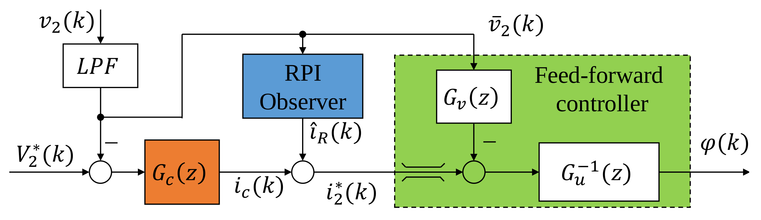
Finally, a combined current feedforward and voltage feedback control system is developed to regulate the secondary terminal voltage.
As shown later, the proposed RPIO can help estimate the load current with the accuracy of higher than
without any current sensors. By feeding-forward the estimated load current to the combined current feedforward–voltage feedback controller, the system dynamics are significantly improved. Voltage fluctuation as well as the setting time are reduced by approximately 50% in the presence of a 30% load change compared to that when the feedforward path is not applied. Computation burden of the proposed RPIO is, however, a little bit increased compared to that of the reduced-order observer reported in [
20] because of a higher order of the observer model (3 vs. 2). Nevertheless, the expensive current sensor is removed and thus efforts to calibrate that noisy signal are also eliminated and economical benefit is also achieved.
2. DAB Small Signal Model
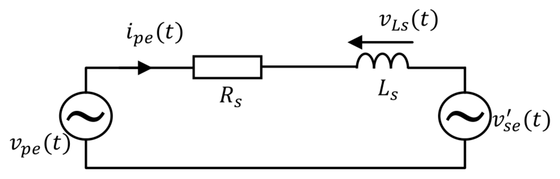
In order to simplify the analysis, the primary referred diagram depicted in
Figure 2 is employed. The Fundamental Harmonic Approximation method is utilized to model the system because of its effectiveness and high accuracy [
22]. In
Figure 2,
,
and
represent the voltages across the primary and secondary windings of the transformer, and the primary current, respectively, which are determined by:
where
and
are terminal voltages;
is the leakage inductance of the transformer;
n is the winding ratio, in this paper,
;
is the angular switching frequency;
and
are the direct and quadrature components of the transferred current; and
is the phase shift.
According to [
23], the large signal model of the DAB converter is:
where
;
is the resistance referred to the primary side of the transformer;
is the load current;
is the output capacitor; and
is the output DC current of the Inverter 2, which is determined by:
In Equation (
2), the phase shift
is the control variable;
and
are system states;
is a state as well as the output; and
and
are the disturbances. The Terminal 1 voltage,
, is usually measured in order for the front-end active rectifier to regulate the MVDC bus. In addition, a large capacitor is usually located at the output of the active rectifier to avoid the double line frequency oscillation. For that reason, in one sampling period, the small variation of
can be assumed to be zero, without loss of the generality.
Next, linearizing Equation (
2) around an operating point, a DAB small signal model can be derived as follows:
where
;
; and
. Here, the lower case notations of the currents and voltage denote small signal quantities whilst the upper case notations express their values at the equilibrium point:
In Equation (
4),
is a disturbance. If it can be compensated, the robustness of the voltage controller can be increased, and the bandwidth of the closed-loop system can be expanded. As a consequence, a faster and better dynamic performance can be achieved. Since the target of this paper is to remove the current sensor,
is thus estimated by using an observer. Therefore, an RPIO is designed in the next section.
3. Observer Design
In this section, a Reduced-order Proportional Integral Observer (RPIO) is designed to estimate the load current. A reduced-order topology is preferred due to its simplicity and feasibility in implementation. PIO is chosen due to its ability for disturbance estimation. Compared to nonlinear disturbance observers, RPIO is simpler with fewer design parameters and has a more explicit model that can be used for other purposes, not only feedforward control.
Equation (
4) can be expressed as:
where
;
;
;
;
;
;
;
;
;
; and
.
The proposed RPIO is then designed as follows:
where
;
;
and
are the observer gain,
and
.
Let
, and
. Since the essence of disturbance
is the load current, its dynamic is usually much slower than the sampling frequency due to the large capacitor at the output side. Therefore, its differentiate can be assumed to be zero in one sampling period, i.e.,
. Then, the dynamic model of the observation error is:
Denoting
;
;
; and
; then
,
and
, and Equation (
8) is rewritten as:
The observability of the error dynamics is verified by checking the rank condition of the observability matrix
. Utilizing the system parameters listed in
Table A1, it is easy to derive that:
Since
, this means that the Equation (
9) is observable. Therefore, the PIO gain
is designed such that matrix
is Hurwitz implying the convergence of the observation error
to zero. This is equivalent to the stability of the matrix
since all eigenvalues of
and
are the same. In addition, the observability of the pair
is equivalent to the controllability of the pair
. Therefore, numerous methods can be used to design
. In this work, the standard linear–quadratic regulator (LQR) method for designing
is employed by considering
and
as a system and input matrix of a dynamical system with the state and input denoted by
v and
w, respectively,
and
is the designed feedback controller for Equation (
10). Then. consider the following performance index:
where
is a positive semidefinite matrix such that
is detectable and
. It is well known in the LQR theory that the controller gain, which stabilizes the Equation (
10) while minimizing the performance index in Equation (
11), is computed by
where
is a positive semidefinite matrix, which is the unique solution of the following Riccati equation:
Note here that the convergence speed of
v is the same as that of
since the eigenvalues of closed-loop systems are the same, as aforementioned. Thus,
and
are designed parameters such that the observation error convergence speed, i.e., the absolute value of the minimum real part of all eigenvalues of
, is as desired, usually two to six times bigger than that of the original system [
24].
After determining the gain
, the observer can be deployed by applying coordinator transformation (
14) to avoid the derivative
in Equation (
6):
where
is the new state variable defined by:
and
are new observer gains and matrices. Block diagram of the proposed RPIO observer with regard to the new state variable is illustrated in
Figure 3. Substituting Equation (
15) into Equation (
6) and Equation (
7),
,
and
can be calculated by:
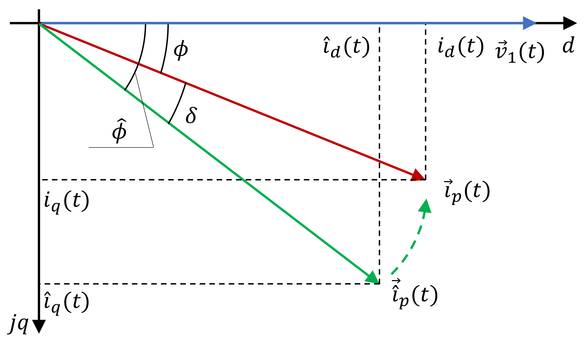
4. Phase Drift Compensation
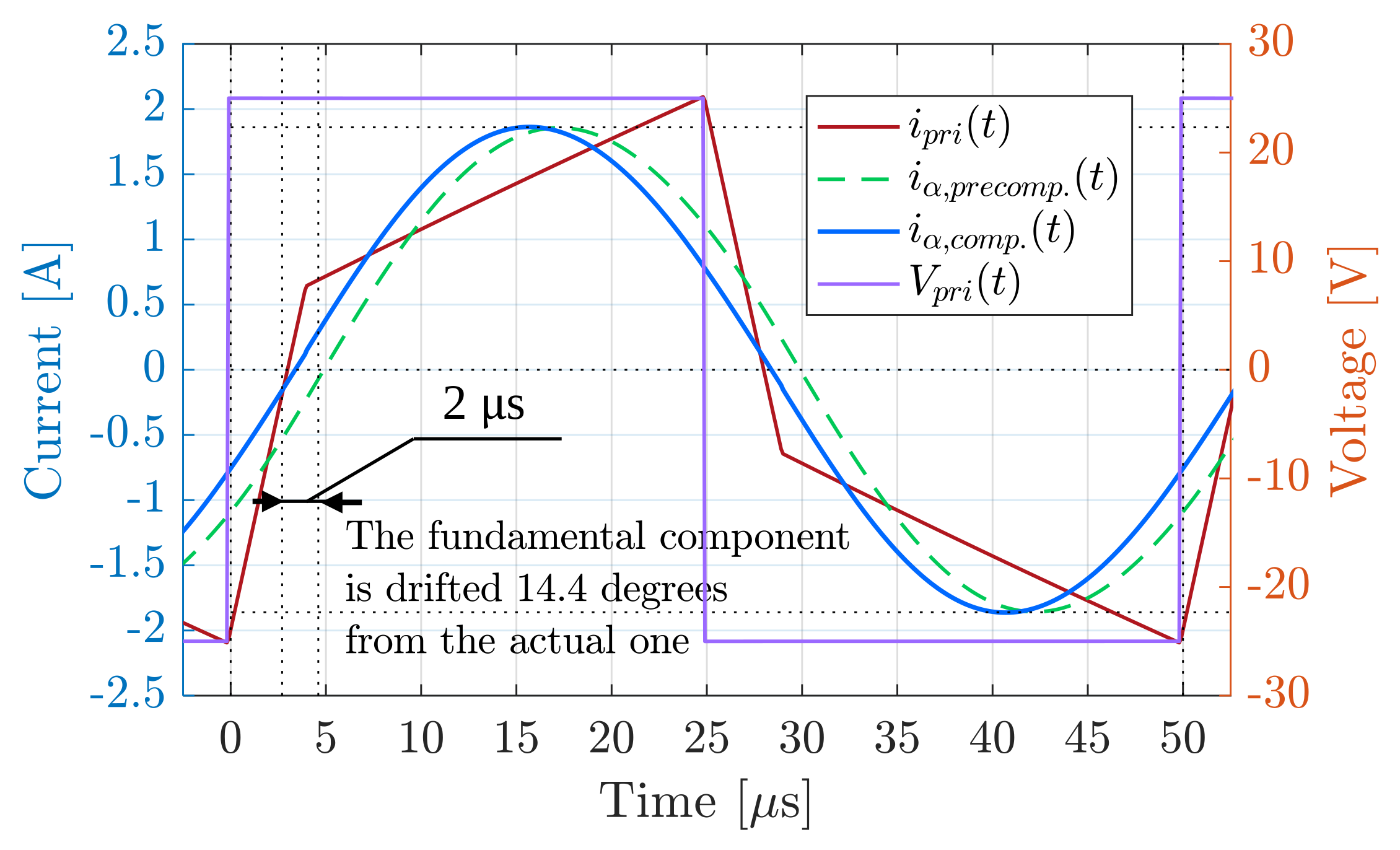
In the best case, the observer designed above can estimate the fundamental components of the primary current and the terminal current with the accuracy of 100%. However, in realistic systems, there is a phase drift between the fundamental current and the actual one when the terminal voltages are not matched.
When the terminal voltages are matched, the current waveform is symmetrical. Hence, the zero crossing point of the current and its fundamental component are coincident. However, when
is other than
, the current waveform becomes distorted. Accordingly, there will be phase lead (
) or lag (
) between the fundamental and the actual load angles.
Figure 4 demonstrates this effect when
V and
V. As seen, in that context, the time lag between the primary current (trapezoidal curve) and the fundamental one (dashed sinusoidal curve) is 2
s (i.e., 14.4 degrees in the angular scale). This error is significant and should be compensated.
According to [
25], the load angle
could be estimated by a simple equation:
As also confirmed in [
25], Equation (
17) can be used to calculate
very accurately with the error less than 2 degrees. Now, denoting
as the estimated load angle obtained by the proposed observer:
Since both
and
can be derived easily, there is no difficulty in calculating the load angle erro
:
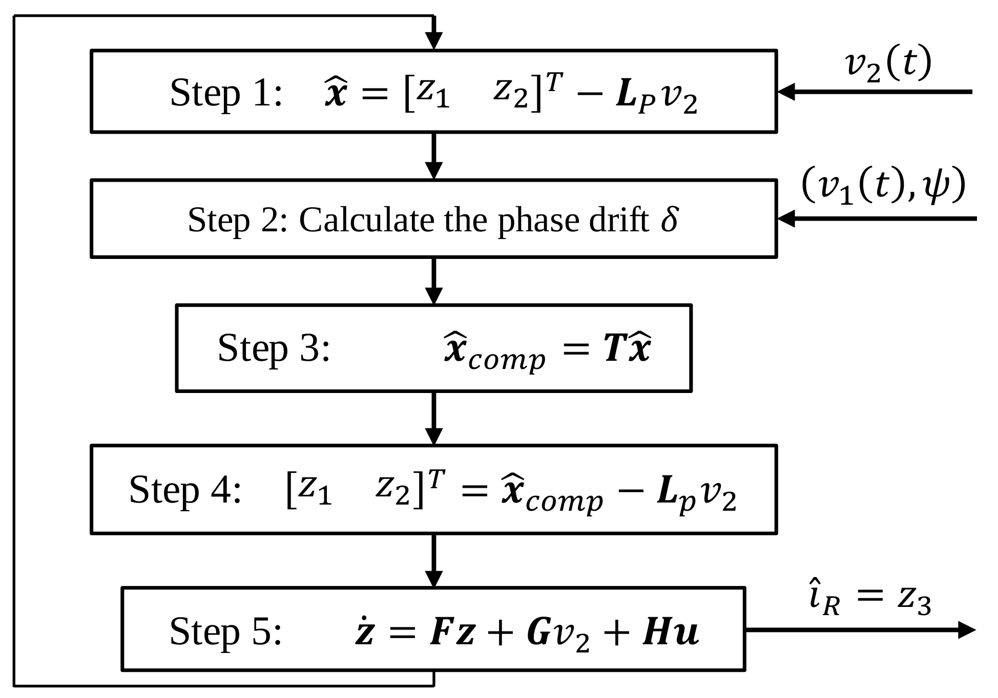
After that, a vector rotation is applied to correct the error in the observed data.
Figure 5 demonstrates the compensation principle. The rotation is accomplished using Equation (
20),
where
is the Park transformation matrix,
. Accordingly, the new system state
should also be updated with regard to the compensation as described in
Figure 6.
Compensation effect is illustrated in
Figure 4. By applying Equation (
20), the compensated fundamental waveform (continuous sinusoidal curve) is shifted backwards to cancel the phase lag. As a result, the phase error becomes insignificant.
6. Simulation and Experimental Results
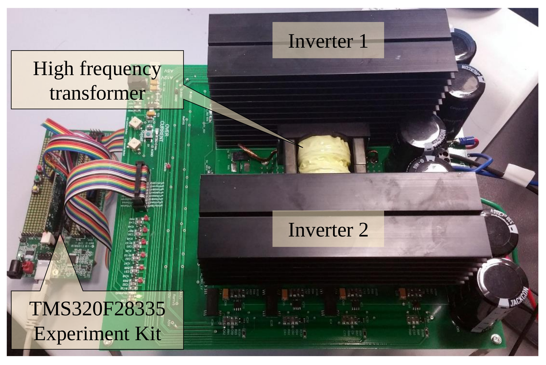
The laboratory scaled experiment system is depicted in
Figure 9. A summary of system parameters is shown in
Table A1. A programmable power supply configured at constant voltage mode is connected to Terminal 1, whereas a DC electronic load is connected to Terminal 2. The winding ratio of the transformer is 1:1. The primary referred leakage inductance and resistance measured at 20 kHz is 67.5
H and 50 m
, respectively.
Aiming to compare among methods, the terminal currents are also measured by using two shunt resistors. The voltages across the resistors are then amplified by isolation amplifiers and filtered out by a low pass filter (LPF). Terminal voltages are also determined in the same manner using voltage divider, isolation amplifier and LPF. The amplifier used in the experiment is a Broadcom ACPL-C79A precision isolation amplifier with 200 kHz bandwidth , hence the amplitude and phase of the measured voltage and current could be ensured.
A TMS320F28335 experiment kit from Texas Instrument is used to deploy the proposed observer and control system designs. Modulation frequency is fixed at 20 kHz. Sampling rate is the same as the switching frequency. In order to ensure the accuracy of the measured terminal current (for comparison purpose), the Analog-to-Digital rate is set to 100 kHz. The data is then averaged after every five samples.
6.1. Simulation Verification
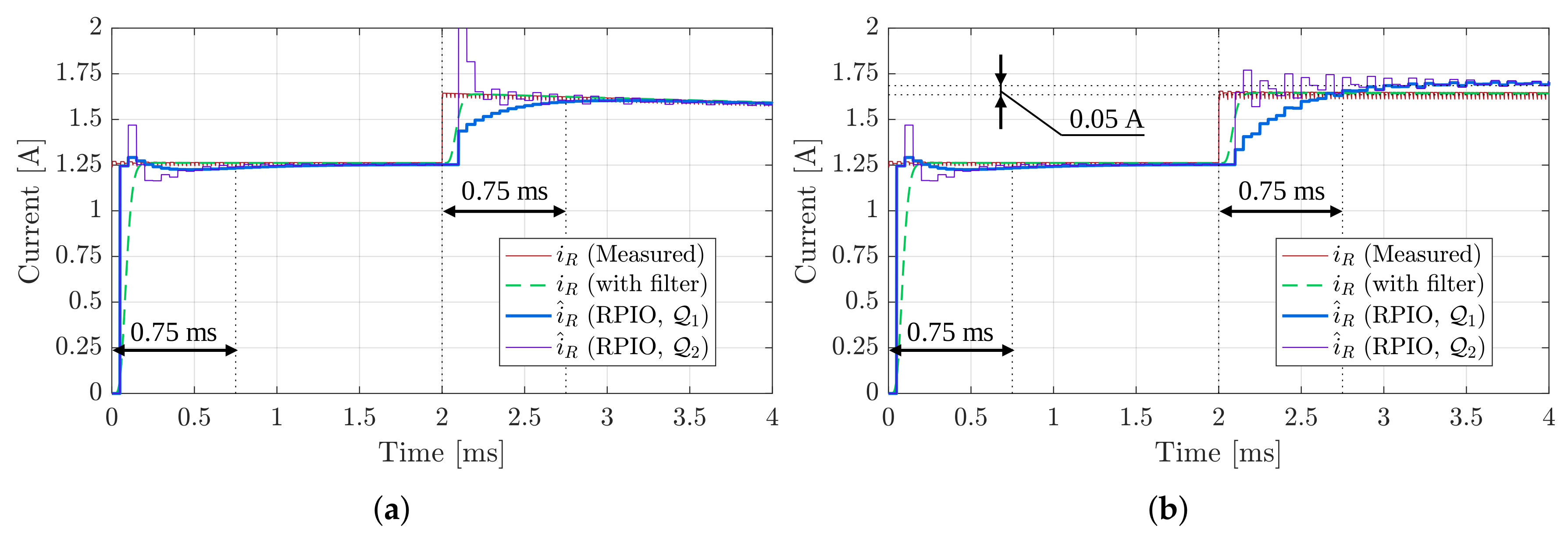
Simulation study is conducted to examine the impact of variable changes as well as the influence of designed parameters on the observation performance in the transient state.
Figure 10a,b illustrates the simulation results as the phase shift and terminal voltage change, respectively. Input voltage is set at 25 V; the phase shift is 30 degrees. At initialization, the load resistance is nominal at 20
, hence output voltage is 25 V as well.
Since
, in this paper,
is assigned to be 1 to simplify the designing process. Two different matrices
and
are used to find the observer gain and matrices:
where
is the
identity matrix.
In the first simulation, after 2 ms, the load resistance is suddenly stepped down by 25% (load increased by 1.33 times) while the phase shift remains constant. As a consequence, output voltage reduces gradually. As seen in
Figure 10a, the observer output, either obtained by designing with
(blue curve) or
(violet curve), matches the load current (red curve) within 0.75 ms. When the voltage reduces, the observed current still adheres to the actual one very well.
The phase shift is changed correspondingly to the change of the load in the second simulation. As the load jumps up, the phase shift is also increased to 42 degrees (40%) to keep the terminal voltage stable. The output of the observer, either obtained by designing with
(blue curve) or
(violet curve), converges after 0.75 ms. There is a steady state error of 0.05 A (see
Figure 10b) in the observed current compared to the simulated one. This means that the observer can estimate the terminal current with the accuracy of approximately 97%.
In both simulation cases above, the observer designed with
responses much faster than when it is designed with
. Theoretical calculation shows that the eigenvalues of the observer obtained by
and
defined above using LQR method are:
where
. Since all poles of
are closer to the origin of the discrete domain than the correspondences of
, it is easy to comprehend the fast response of the RPIO when designed with
rather than with
.
The convergence time could be further reduced by increasing the value of matrix
in the LQR method, i.e., placing eigenvalues of the observer closer to the origin. However, there is a trade-off between robustness and dynamic response. A higher value of
results in a faster but more sensitive observer. On the contrary, a smaller
brings more robust observation performance, but slower response time as indicated in
Figure 10a,b.
From the above simulation verification,
is chosen as the design parameter for better robustness of the proposed RPIO. Accordingly, observer gains are:
Substituting the above
and
into Equation (
16), then matrices
,
,
can be yielded as listed in
Table A2. Note that, although Equation (
16) is derived in the continuous domain, it can also be used for deriving
,
, and
without losing the correctness.
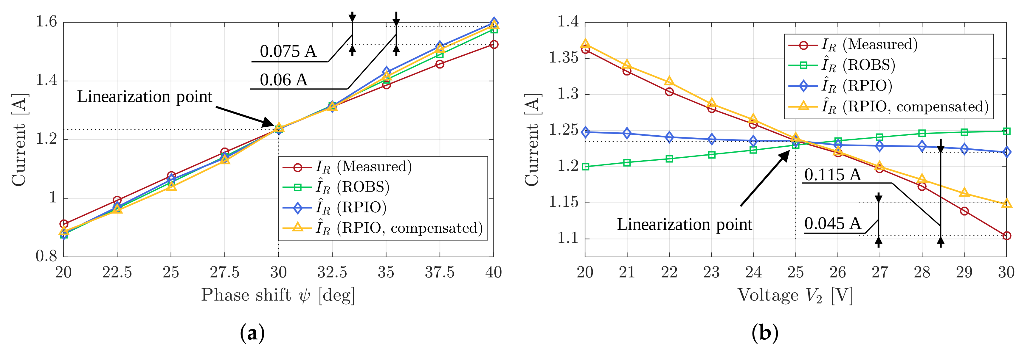
6.2. Open-Loop Experimental Verification
This experiment is conducted to verify the static performance of the proposed observer.
Figure 11a,b illustrates the output responses of the proposed observer (RPIO), designed with
defined above, in comparison with the actual values and with the reduced order observer (ROBS) , which was designed in [
20] based on the Terminal 1 current under some different operating conditions.
First, Terminal 2 voltage is fixed at its nominal by setting the DC electronic load to constant voltage mode. The phase shift is then gradually increased from 20 to 40 degrees (
around the linearization point). As shown in
Figure 11a, all four curves are very close to each other. The estimation error is unremarkable when
degrees. The error is greatest when
is 40 degrees. At that condition, the measured current (red, circle marked) is about 1.53 A, whereas the estimates by ROBS (green, square marked) and RPIO (blue, diamond marked) are 1.58 A and 1.60 A, respectively. In other words, the estimation error is about 5%. Because the error is already small, applying the compensation in Equation (
20) does not contribute to a big but minor reduction on the estimation error to 4%. This result is similar to the simulation study described above.
Next, Terminal 2 voltage is varied with a step of 1 V while fixing other parameters. Results shown in
Figure 11b suggest that, in practice, the observation performance seems to be more sensitive to the voltage changes than the phase shift changes. The error is about
A when applying ROBS. Employing RPIO (non-compensated) helps reduce the error to
A, which is still quite remarkable. This is because of the phase drift phenomenon mentioned in the previous section. By using the proposed compensation method, the estimation error is much more reduced. The maximum error is now only 0.045 A, which is more than three times reduction compared to that obtained by ROBS.
Another quantitative comparison can be conducted regarding the
coefficient (coefficient of determination). Accordingly, when varying the phase shift while keeping terminal voltages constant (
Figure 11a), the
of the three observations are
(RBOS),
(RPIO) and
(RPIO with phase drift compensated). There is no significant differences between the three observer results. Nevertheless, when terminal voltages are not matched, RPIO brings a remarkable performance improvement. With the experimental data shown in
Figure 11b, the
are
(RBOS),
(RPIO) and
(RPIO with phase drift compensated). Obviously, applying the proposed RPIO can help to improve the observation accuracy by approximately 2%. If the phase drift phenomenon is compensated, the improvement is even higher at nearly 2.5%. That is to say, the proposed observer accompanied with the compensation method can estimate the Terminal 2 current with the accuracy of more than 98%.
Although containing some division and trigonometric functions, compensator in Equation (
20) executes pretty fast on DSP F28335. At a 150 MHz system clock, the observer (including compensation procedures) takes only
s to accomplish. The executing time can be further reduced by optimizing the programming or using a lookup table for trigonometric functions. Since the sampling time is
s, there is plenty of time for other functions and algorithms such as PI calculation or communication, etc. This also provides possibility to increase the sampling frequency to more than 100 kHz if required.
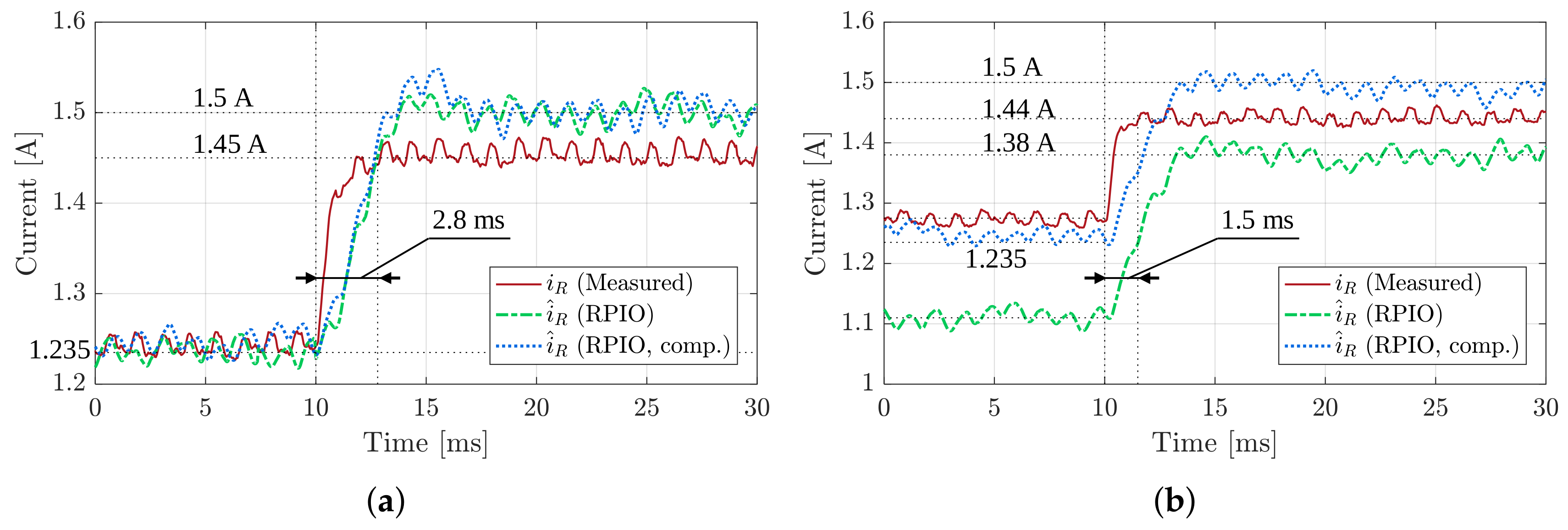
6.3. Feedforward Current Loop
With
and other observer gains and matrices as listed in
Table A2, the feedforward current controller is derived as shown in
Table A3. In this experiment, the DC electric load is still configured to the constant voltage mode at 25 V. Only the current loop is examined. At first, the reference current is set to the nominal of 1.235 A. After some time, it is increased by 20% to 1.5 amperes. The current responses are then displayed in
Figure 12.
The measured current (denoted by the red, solid curve) is well stabilized around 1.235 A (i.e., at the nominal condition). In this context, the observer can also estimate the current very precisely. The dashed (original RPIO) and dotted (RPIO with compensation) curves are mostly coincident with the actual one in the interval from 0 to 10 ms (
Figure 12a). When the reference current steps up, the current responds quickly to reach its stable state after 2.8 ms. Although the observation values match the set-point, the actual average current is only 1.45 A. Therefore, a steady state error of 0.05 A exists. Since the voltages across two terminals are equal, there is no significant difference between the original RPIO and RPIO with compensation performances.
Figure 12b shows the current response when terminal voltages are not matched (e.g.,
V and
V). When the current command is 1.235 A, the terminal current is about 1.275 A. When the command increases to 1.5 A, the terminal current settles down after 1.5 ms at 1.44 A. The steady state errors are
A and
A, respectively, which are relatively small (
4%). As for the observed current, the observation error is remarkable without compensation as discussed above. When the compensation method is applied, the same result as the one obtained when the voltage ratio is unity can be achieved.
6.4. Voltage Loop
In this section, the dynamic performance of the voltage control system is investigated. There are two experiments: load increase and load decrease. The Terminal 1 voltage is fixed at 25 V. The DC electronic load operates in the constant resistance mode. The reference for the voltage control loop is 25 V. Both static and dynamic performances of the voltage loop are considered in two cases: with and without the feedforward path. The output of the RPIO is employed for feeding forward to the output of the voltage controller that makes the system a feedforward controller (FFC). Note here that the estimated load current
is phase-drift-compensated. In the second case, the feedforward path is ignored, and hence the control system behaves as a normal voltage mode controller (VMC). In both cases, the same PI controller as shown in
Table A3 is employed.
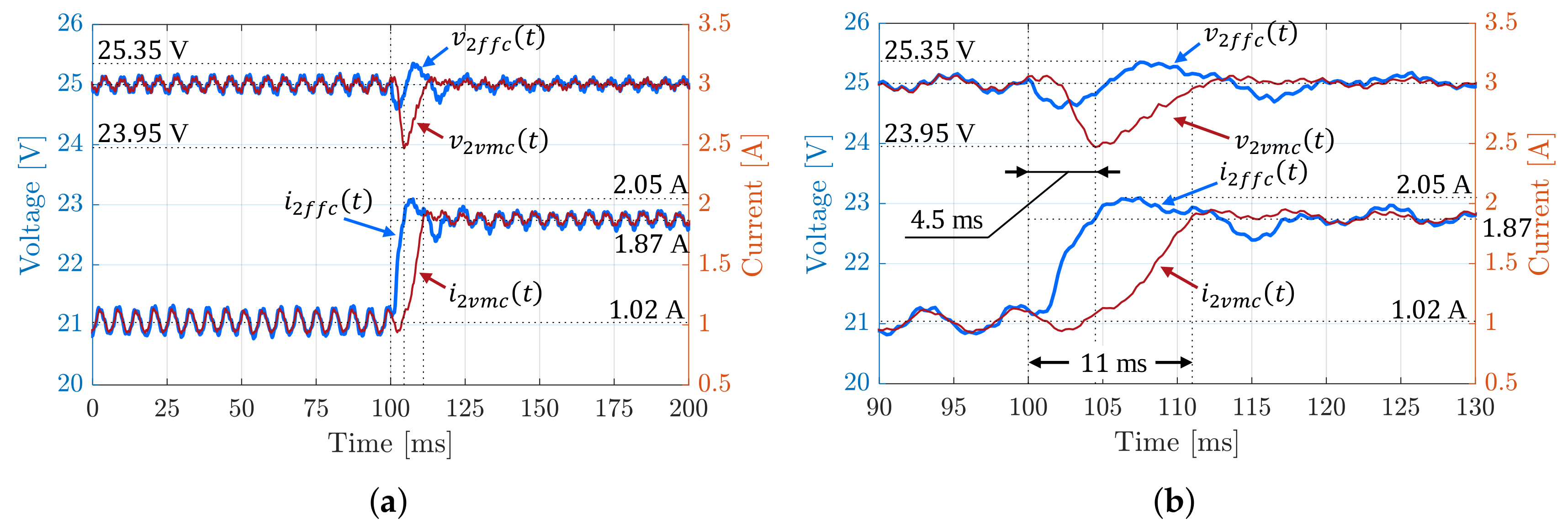
At first, the resistance is set to 25
, which is 1.25 times greater than its nominal (20
). After some time, the resistance is suddenly reduced to 13.3
(
reduction).
Figure 13a shows the voltage and current waveforms in the full-time scale and
Figure 13b provides a zoomed-in view of the transient period. As seen, the voltage is well regulated regardless of with or without the feedforward path. When the load suddenly increases, there is a sag of 1.05 V (i.e., 4% of the set-point) in the voltage responses when VMC is employed. After 11 ms, the voltage is restored and stabilized at the desired value. Since the voltage controller is of the PI type, there is no steady state error. When a feedforward path from the RPIO is applied, dynamic performance is significantly improved. The voltage fluctuation is mostly suppressed as the maximum variation is only
V, or 1.4% in the per unit (pu.) scale. The settling time is also much reduced from 11 ms to only 4.5 ms.
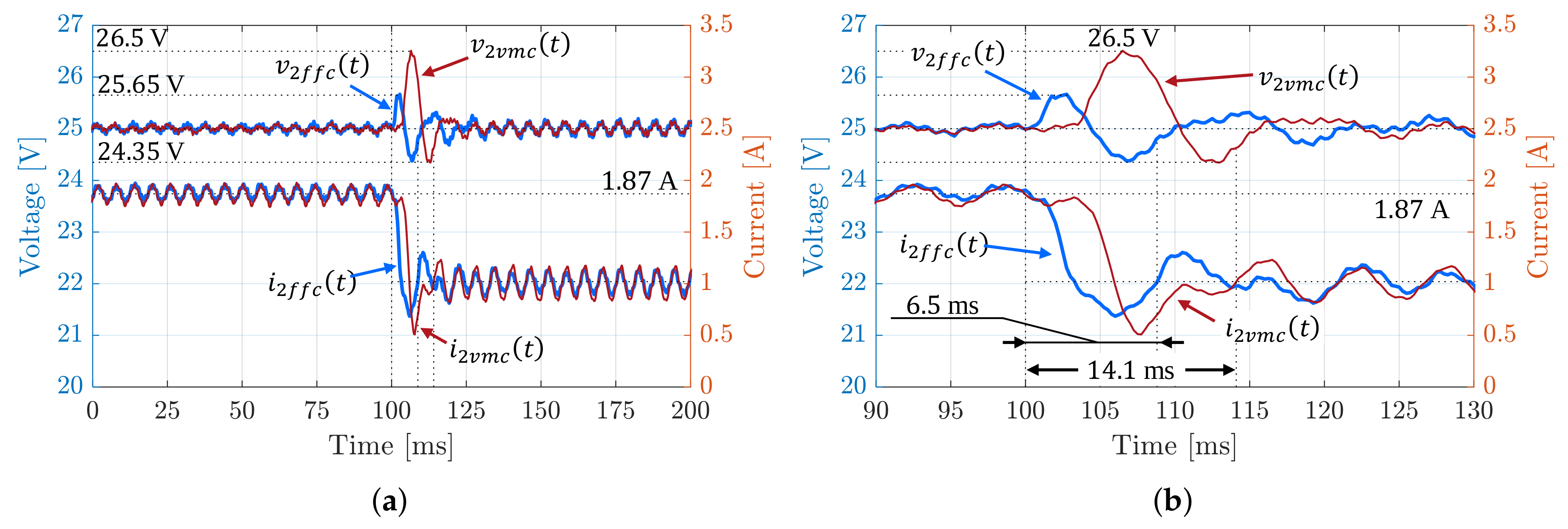
The same effect is observed when decreasing the load. In this experiment, the load change scenarios are reversed. The load resistance is initialized at 13.3
then after a while is suddenly increased to 25
.
Figure 14a,b shows the voltage and current waveforms in the full-time and zoomed-in scales.
Without the feedforward path, the voltage swell is 1.5 V or 6% in the per unit scale. The settling time is also relatively long at 14.1 ms. By utilizing our proposed control system, the voltage variation reduces more than 50% to only V (or 2.6% in pu.). Response speed is about two times faster as the voltage settles down after only 6.5 ms.
7. Conclusions
This paper proposes a new observer-based control system for the dual-active-bridge converter. More specifically, a reduced-order proportional integral observer (RPIO) is designed to estimate the terminal current instead of measuring it. In addition, a compensation technique is introduced to reduce the phase drift phenomenon due to the current distortion waveform. Simulation and experimental results show that the observation accuracy is more than 98%. Compared to the observer designed in [
20,
21], the observation performance is significantly improved.
A current feedforward and voltage feedback control system are then developed to regulate the Terminal 2 voltage. As a consequence, the dynamic performance is remarkably improved. The voltage fluctuation can be almost ignored and the response speed is two times faster.
Moreover, the proposed RPIO can estimate not only terminal current, but also the load angle, the direct and the quadrature components of the AC current, with high accuracy. Those estimated values can also be used for other control topologies—for example, the decoupled current control [
20]. Therefore, not only is the system dynamic enhanced, but the overall efficiency can also be improved by reducing the reactive power (proportional to the quadrature current).
The above outcomes are achieved with only the information of the terminal voltages. Besides the economical benefit of removing current sensors, efforts for increasing the processing speed and suppressing the noisy current signal are also eliminated. Furthermore, the implementation of the proposed RPIO is also simple and feasible as the computing time (including phase drift compensation) is only 2.86 s. This means that this technique can be applied for a much faster dual-active-bridge converter system.


