Article

Cascaded Multilevel Inverter Topology Based on Cascaded H-Bridge Multilevel Inverter

by
Abdullah M. Noman
1,2,*,
Abdullrahman A. Al-Shamma’a
1,2,
Khaled E. Addoweesh
1,
Ayman A. Alabduljabbar
3 and
Abdulrahman I. Alolah
1
1
Department of Electrical Engineering, Faculty of Engineering, King Saud University, Riyadh 11421, Saudi Arabia
2
Department of Communication and Computer Engineering, Faculty of Engineering and Information Technology, Taiz University, Taiz, Yemen
3
King Abdulaziz City for Science and Technology, Riyadh 6068, Saudi Arabia
*
Author to whom correspondence should be addressed.
Energies 2018, 11(4), 895; https://doi.org/10.3390/en11040895
Submission received: 8 March 2018 / Revised: 30 March 2018 / Accepted: 30 March 2018 / Published: 11 April 2018

Abstract

:
A three-phase multilevel inverter topology for use in various applications is proposed. The present topology introduces a combination of a cascaded H-bridge multilevel inverter with a cascaded three-phase voltage source inverter (three-phase triple voltage source inverter (TVSI)). This combination will increase the number of voltage levels generated when using fewer components compared with the conventional multilevel inverter topologies for the same voltage levels generated. The other advantage gained from the proposed configuration is the assurance of a continuous power supply to the grid in case of failure in one part of the proposed configuration. In addition, the voltage stresses on switches are reduced by half compared if each part in the proposed topology is working independently. The comparison of the proposed topology with some conventional multilevel inverter topologies is presented. The proposed topology is built in the SIMULINK environment and is simulated under various loads in addition to being connected to the grid. Phase-shifted pulse width modulation technique is used to generate the required switching pulses to drive the switches of the proposed topology. The inverter is experimentally implemented in the lab, and the switching pulses are generated with the help of MicroLabBox produced by dSPACE (digital signal processing and control engineering) company. The simulation and experimental results and their comparisons are presented to verify the proposed topology’s effectiveness and reliability.

1. Introduction

The term “multilevel” began when Nabae performed the three-level converter in 1981. In this study, a three-level neutral point clamp (NPC) was proposed [1]. Subsequently, several multilevel converter topologies have been developed [2,3,4,5]. In recent years, many multilevel converter topologies have been proposed and have gained attention in many applications, especially in the interface for the grid connection of photovoltaic (PV) systems [3]. The most common multilevel inverter (MLI) topologies can be classified into three types: neutral point MLI, flying capacitor MLI, and cascaded H-bridge (CHB) MLI.
The cascaded H-bridge multilevel inverter (CHB-MLI) is based on the series connection of the H-bridge inverters. It is an alternative topology with fewer switches when compared with other MLI topologies of the same voltage level. Each H-bridge can be used to generate three output voltage levels by a unipolar modulation technique. CHB-MLI has been used for renewable energy sources, especially PV modules, due to its separate Direct Current (DC) source feature. Cascaded H-bridge MLI features have proved to be an attractive solution for many applications, such as standalone systems [5], volt ampere reactive (VAR) compensations, and grid-connected PV systems as presented in [6,7,8,9].
Generally, the cascaded H-bridge topologies have received more attention. The cascaded H-bridge inverter has a simple layout, extreme modularity, a simple construction, control, and no voltage balance problems, and compared with the other multilevel topologies, it requires the fewest components for generating the same voltage levels [10,11,12]. However, if more levels are required to improve the current and voltage’s quality, the number of switches can be increased. Increasing the number of switches can lead to an increase in the cost, the conduction, and the switching losses, thus reducing the system efficiency. The reliability will also be reduced when the number of switches is increased, and the control system will be more complex.
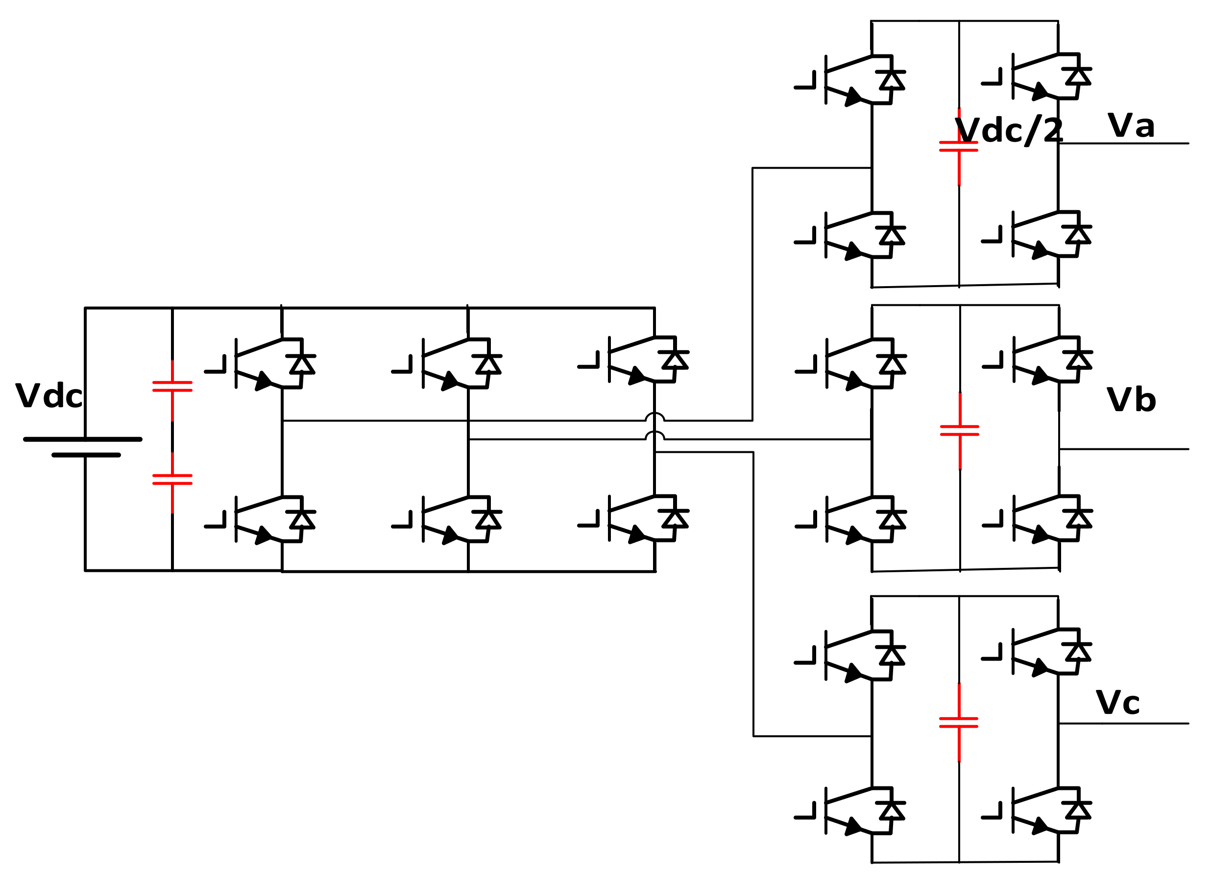
Many other cascaded inverter topologies have been proposed to increase the number of voltage levels generated, which will improve the system’s performance and reduce cost [10]. Asymmetrical CHB-MLI topologies have been proposed to increase the number of levels by combining various ranges of voltage DC sources as shown in Figure 1 [13,14,15]. In these topologies, the number of levels increase, but the stresses on the switches are not equal. The stress on switches connected to the lower DC input voltage will be lower than that on switches connected to the higher DC input voltage. Unequal loss sharing among switches will cause varying temperatures for switches, and some switches may be burnt. In addition, unequal loss sharing means different voltage ratings will be used for switches, which results in a higher cost. On the other hand, unequal loss sharing requires switches with higher voltage ratings.
On the other hand, modified topologies have been proposed based on CHB to improve the output voltage quality [16,17], but the advantages of the CHB are lost, such as simplicity, simple construction, simple control, and modularity.
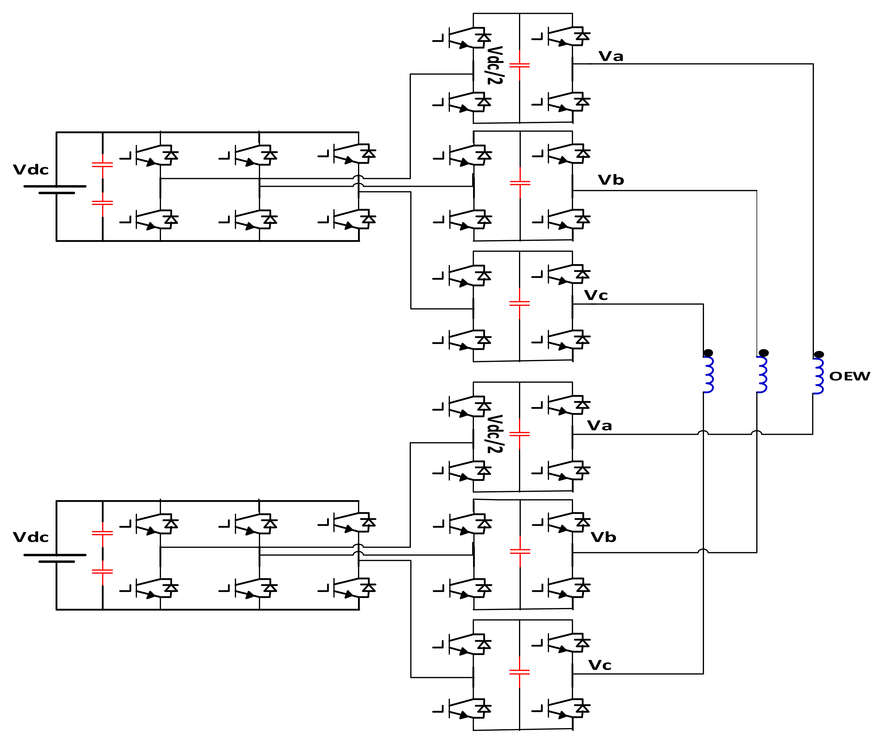
Hybrid multilevel inverter topologies were proposed based on three-leg two-level inverter with CHB [18,19,20,21,22]. The hybrid multilevel inverter topology is shown in Figure 2. The authors in [18] proposed a five-level inverter topology based on two-level and floating capacitor H-bridge cells. The proposed inverter topology can be operated as a three-level inverter for the full modulation range, in case of any switch failure in the capacitor-fed H-bridge cell. This will increase the system’s reliability. The authors [22] also proposed a nine-level inverter topology based on a conventional hybrid two-level voltage source inverter (VSI) with CHB-MLI using open-end winding (OEW) transformers as shown in Figure 3. These topologies are not reliable, however, because they are based on a two-level three-leg inverter. The inverter system will be out of work if this two-level inverter malfunctions, and the power will not be supplied to the grid. In these topologies, the H-bridges are connected to floating capacitors whose voltages should be controlled carefully to be maintained at required asymmetrical values. This adds more complexity to the control algorithm.
Another type of cascaded MLI topology is based on the conventional two-level voltage source inverter. It has been used in many motor-drive applications as shown in Figure 4 [23,24]. This cascaded MLI can also be used for grid-connected renewable energy applications [23,24,25]. The author in [23] used this topology to connect the wind farm to the grid, whereas others [25] used the three-phase cascaded VSI for grid-connected PV applications. However, the three-phase currents in each unit are not balanced, which means the current stresses on each leg are not equal. The authors in [26] solved the problem of unbalanced three-phase currents in each unit by using inter-mediate transformers instead of inductors as shown in Figure 5.
However, the inter-mediate transformers are bulky [27]. On the other hand, in both topologies, the number of voltage levels will be limited due to the limitation in the number of cascaded VSI units.
In this paper, a proposed multilevel inverter configuration introduces a combination of the cascaded H-bridge multilevel inverter and the three-phase cascaded VSI. This combination will increase the number of voltage levels generated from the inverter while using fewer components than the conventional multilevel inverter topologies do for the same voltage levels. The proposed topology is built in the SIMULINK environment (2016a, MathWorks), is simulated under various loads, and is connected to the grid. In Section 2, the proposed topology is described. In Section 3, the analysis of the proposed topology is explained. To validate the good performance of the proposed topology, the simulation results are shown in Section 4. In Section 5, the experimental setup, and the experimental results are demonstrated.

2. Description of the Proposed Topology

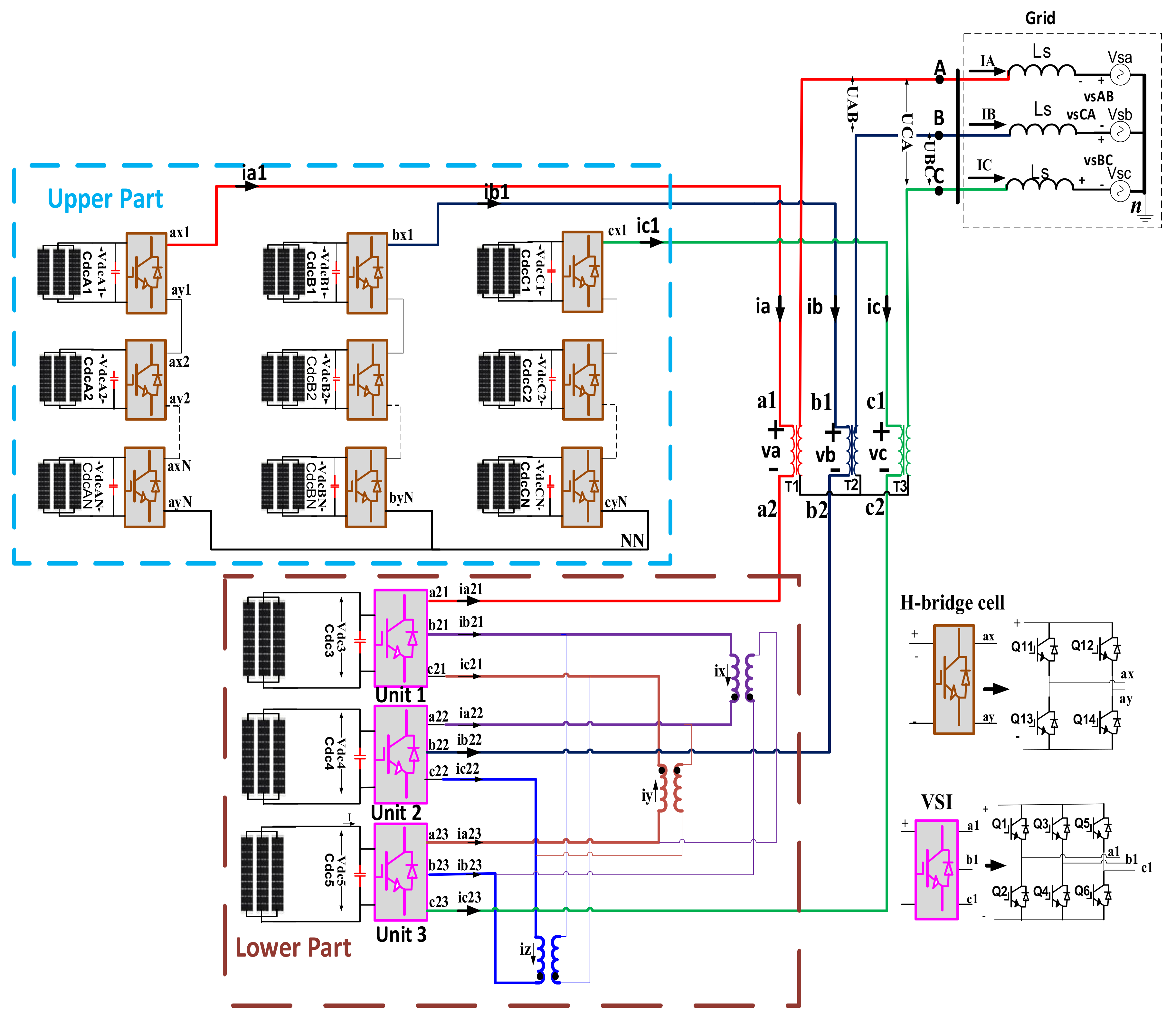
The present topology relates to a three-phase multilevel high-voltage/high-power converter, which is a hybrid configuration that conjoins two conventional multilevel configurations: a cascaded H-bridge MLI and a three-phase cascaded VSI (can also be called three-phase triple VSI (TVSI)). Figure 6 reveals the proposed cascaded MLI topology. This new topology can be used for numerous grid-connected applications, such as grid-connected PV systems, power factor correction, and static VAR compensation.
The proposed topology can be used to generate any number of voltage levels using fewer components compared with the conventional multilevel inverter topologies. The proposed inverter topology consists of two parts, which are connected together with open-end winding transformers as shown in Figure 6. To better describe the proposed inverter topology, it has been divided into two parts. The upper part is the cascaded H-bridge MLI, and the lower part is the three-phase triple VSI.
First: Description of the upper part: This part consists of three-phase systems. Each phase consists of N H-bridge cells. These cells are cascaded as shown in the upper part of Figure 6 such that the a y 1 terminal of H-bridge cell 1 in phase a, for example, is connected to the a x 2 terminal of the next H-bridge cell. In addition, the a y ( N 1 ) terminal is connected to the a x N terminal of the last H-bridge cell. The same idea is applied phases b and c. The terminals of a y N ,   b y N , and c y N of phases a, b, and c are connected together to one point, NN.
Second: Description of lower part: The three-phase triple-voltage source inverter consists of three units. Each unit is a three-leg two-level inverter, and the three units are cascaded as shown in the lower part of Figure 6. Each unit consists of three terminals: a 2 k , b 2 k ,   and   c 2 k where k is the unit number. The three units are cascaded with one another by using coupled inductors as shown in the lower part of Figure 6. The coupled inductors are used instead of inter-mediate transformers in the lower part.
Finally: The upper and lower parts are connected in such a way that phase a of the upper configuration is connected to phase a of the lower configuration via open-end winding. Terminal a x 1 from the upper part is connected to terminal a 1 of open-end winding transformer T 1 , and terminal a 21 of unit 1 in the lower part is connected to terminal a 2 of open-end winding transformer T 1 . The same idea is applied for open-end winding transformers T 2 and T 3 . The secondary windings of transformers T 1 , T 2 , and T 3 are then connected to the three-phase grid. Three single-phase line frequency transformers presented in the proposed topology are used to connect the upper three-phase cascaded H-bridge inverter with the lower three-phase triple voltage source inverter. The operation of the three single-phase transformers are based on the principles of the open-end transformer. The open-end winding transformer has gained advantages to the MLI topologies: (1) The voltage rating of the power devices is reduced by half; (2) the size of the capacitors is reduced; and (3) the DC bus magnitude that the PV modules provide can be reduced by half compared with if only one part (upper or lower) is used. This topology generates higher voltage levels by reducing the number of required switches compared with the conventional multilevel inverter topologies for the same voltage levels. The reduction in the switches leads to a reduction in complexity and dimensions of the converter. In addition, the topology helps reduce the total harmonic distortion (THD) of the voltages and currents. Another important advantage of the proposed inverter topology is that in case of failure in one part, the other part will work independently, and the power will still be available. In addition, if more levels are needed, the number of H-bridge cells in the upper part can be increased. The concept presented in this paper is validated by means of simulation and experimental results.
The advantages of the invention can be summarized as follows:
  • More levels can be obtained by using fewer switches compared with the conventional multilevel inverter topologies for the same voltage levels.
  • Voltage and quality of current can be improved.
  • A continuous power supply to the grid is assured in the case of failure one configuration. Therefore, the proposed topology is reliable.
  • The voltage stresses on switches are reduced:
  • Stresses on the upper switches:
    2 V 2 N 3
    where V is the root-mean-square (RMS) of the line–line grid voltage, and N is the number of cascaded H-bridge cells.
  • Stresses on the lower switches:
    2 V 6 3
  • Equal Current stresses on switches. The current stress on all switches in the proposed topology is the RMS grid current I .

3. Analysis of the Proposed Topology

3.1. Voltage Relationships

The analysis of the circuit voltage on the primary side of the open-end winding transformers shown in Figure 6:
For phases a–b:
v a x y v a v a 21 b 21 v b 21 a 22 v a 22 b 22 + v b v b x y = 0
For phases b–c:
v b x y v b v b 22 c 22 v c 22 b 23 v b 23 c 23 + v c v c x y = 0
For phases c–a:
v c x y v c v c 23 a 23 v a 23 c 21 v c 21 a 21 + v a v a x y = 0
where:
v a x y = v a 1 ,   v b x y = v b 1 , and v c x y = v c 1
Therefore:
v a b = ( v a 1 v b 1 ) v a 21 b 21 v b 21 a 22 v a 22 b 22
v b c = ( v b 1 v c 1 ) v b 22 c 22 v c 22 b 23 v b 23 c 23
v c a = ( v c 1 v a 1 ) v c 23 a 23 v a 23 c 21 v c 21 a 21
The line-line voltage of the lower part is given as follows:
v a 2 b 2 = v a 21 b 21 + v b 21 a 22 + v a 22 b 22
Due to the transformer action in the lower part:
v b 21 a 22 = v a 23 b 23
Equation (6) can be written as follows:
v a b = v a 1 b 1 v a 2 b 2
v b c = v b 1 c 1 v b 2 c 2
v c a = v c 1 a 1 v c 2 a 2
where v a 1 b 1 , v b 1 c 1 and v c 1 a 1 are the line-line voltages of the upper part; v a 2 b 2 , v b 1 c 1 and v b 1 c 1 are the line-line voltage of the lower part. The generated line-line voltages from the proposed topology are given as:
[ v a b v b c v c a ] = [ U A B * U B C * U C A * ] = 3 m a ( 3 2 V d c + N V d c / H B )   [ sin ( w t + 30 ) sin ( w t 90 ) sin ( w t + 150 ) ]
where N is the number of H-bridge cells connected to each phase, V d c / H B is the DC link voltage for each H-bridge cell, V d c is the DC link voltage across each unit in the lower part, U A B * is the line-line voltage in the secondary side of the transformer referred to the primary side (assume 1:1 turns ratio), and m a is the modulation index.
Equation (10) can be combined using instantaneous space vector, defined as [28]:
v L L = 2 3 [ v a b + a   v b c + a 2   v c a ] = 2 V L L e + j ( w t + 30 )
where V L L = 3 2 m a ( 3 2 V d c + N V d c / H B ) , a = e j 2 π / 3 , and a 2 = e j 4 π / 3 .
If it is assumed that V d c = V d c / H B , the RMS line-line voltages of the proposed topology can be given as:
V L L = 3 2 2 m a V d c ( 3 + 2 N )
This means that the generated line-line voltage equals ( 3 + 2 N ) times the line-line voltage of each two-level VSI unit. If N = 2, the RMS line-line generated voltage is seven times the line-line voltage of each VSI unit.
The space vector of the generated voltage across the open-end windings v O E W is given as follows:
v O E W = 2 3 [ v a 1 a 2 + a   v b 1 b 2 + a 2   v c 1 c 2 ] = m a ( 3 2 V d c + N V d c / H B ) e + ( j w t )
where V a 1 a 2 ,   V b 1 b 2 ,   and   V c 1 c 2 are the voltages across the primary sides of the transformers T 1 ,   T 2   and   T 3 , respectively.

3.2. Current Relationships

The instantaneous space vector current i O E W flows through the primary windings of the open-end winding transformers:
i O E W = 2 3 [ 1 + a + a 2 ] [ i a i b i c ] = 2 I e + j ( w t )
where I is the RMS grid current.
The phase currents of each unit in the lower part of Figure 6 satisfy the following equations:
[ i a 21 + i b 21 + i c 21 i a 22 + i b 22 + i c 22 i a 23 + i b 23 + i c 23 ] = 0
The currents of each unit in the lower configuration of Figure 6 can be expressed as follows:
[ i a 21 i b 21 i c 21 ] = [ i a 22 i b 22 i c 22 ] = [ i a 23 i b 23 i c 23 ] = [ i y i x i x i z i z i y ]
where i x ,   i y ,   and   i z are the currents flowing in the primary windings of the coupled inductors as shown in Figure 6.
Assuming that the magnetizing inductance of the coupled inductors are high such that the circulating current is zero:
i x + i y + i z = 0
Using (14), (16), and (17), the instantaneous space vector current i x y z flowing in the primary windings of the coupled inductors can be expressed as follows:
i x y z = 2 3 [ 1 + a + a 2 ] [ i x i y i z ] = 2 3 I e + j ( w t + 30 )
Substituting (18) into (16), the instantaneous space vector current i L o w in each unit in the lower part can be given as follows:
i L o w K = 2 3 [ 1 + a + a 2 ] [ i a 2 K i b 2 K i c 2 K ] = 2 I e + j ( w t + 180 )
where K could be 1, 2 or 3, which represents unit 1, unit 2, or unit 3, respectively.
As shown from (1) and (19), the current stress on all switches in the proposed topology is I, where I is the RMS grid current.

3.3. Power Relationships

The apparent powers of units 1, 2, and 3 in the lower part are as follows:
[ V A U 1 V A U 2 V A U 3 ] = ( 3 2 2 m a V d c ) [ I a , r m s I b , r m s I c , r m s ]
where V A U 1 , V A U 2 , and V A U 3 are the apparent power of units 1, 2 and 3 respectively. In addition, I a , r m s , I b , r m s , and I c , r m s are the RMS currents of phases a, b, and c, respectively.
The total apparent power of N cascaded H-bridge cells in each phase is as follows:
[ V A a V A b V A c ] = ( N m a 2 V d c / H B ) [ I a , r m s I b , r m s I c , r m s ]
where V A a , V A b , and V A c are the apparent power N cascaded H-bridge cells connected to phase a, b, and c, respectively.
The total apparent power of the proposed topology can be given as follows:
( V A T ) = 3 ( N m a 2 V d c / H B ) I r m s + ( 9 2 2 m a V d c ) I r m s = 3 2 m a I r m s ( 1.5 V d c + N V d c / H B )
From another point of view, the total apparent power of phase a of the proposed topology can be given as follows:
( V A T A ) = V a 1 a 2 I a , r m s = 1 2 m a I a , r m s ( 1.5 V d c + N V d c / H B )
Similar for phases b and c, we get:
( V A T B ) = V b 1 b 2 I b , r m s = 1 2 m a I b , r m s ( 1.5 V d c + N V d c / H B )
( V A T C ) = V c 1 c 2 I c , r m s = 1 2 m a I c , r m s ( 1.5 V d c + N V d c / H B )
This means that each unit in the lower part and the cascaded H-bridge cells have connected to share the same amount of output power.

4. Simulation Results

The proposed inverter topology shown in 
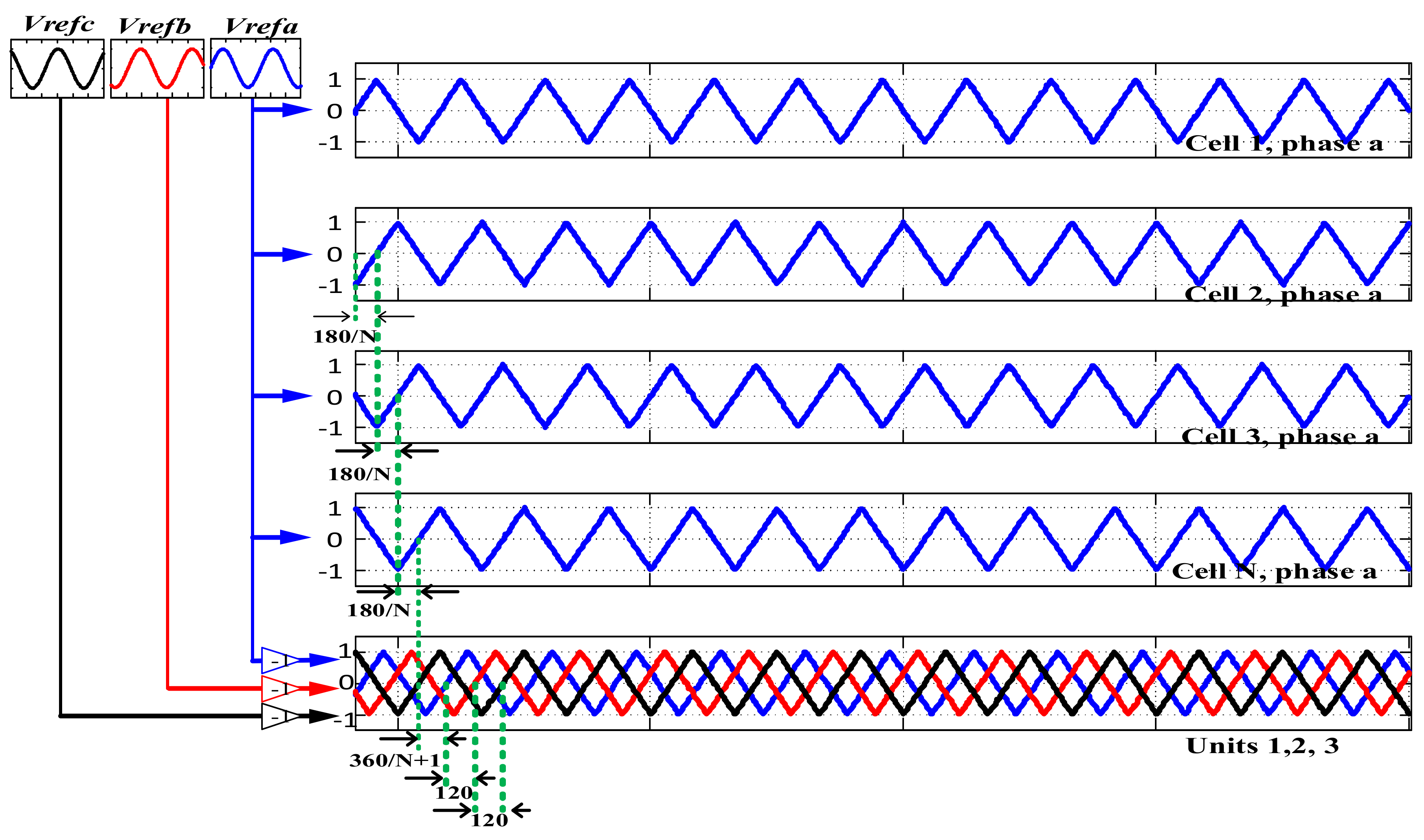
Figure 6 is built in SIMULINK, and the simulation is achieved using the MATLAB/SIMULINK environment (2016a, MathWorks). For simplicity, two cascaded H-bride cells are used in each phase in the upper part of the proposed topology. The magnitude of the DC voltage used for each cell in the upper and lower parts is 30 V. phase-shifted pulse-width modulation (PWM) technique (PSPWM) is used to generate the required pulses of the insulated-gate bipolar transistors (IGBTs). In this technique, the reference signals are used to generate switching pulses to drive the IGBTs of the proposed topology by comparing them with the generated triangular carrier waveforms as shown in Figure 7. The reference signals are three-phase sine waveforms whose frequencies are 60 Hz. As shown Figure 7, the phase-shift technique is used to generate the pulses to drive the IGBTs of the cascaded H-bridge part (upper part), as the triangular signal of the next H-bridge cell is shifted from the previous H-bridge by 180 / N , where N is the number of H-bridge cells. Reference voltage signal V r e f a is compared with these phase-shifted triangular waveforms, and the resulting pulses are used to drive the IGBTs of the H-bridge cells of phase a.
In addition, reference voltage signals V r e f b   and   V r e f c are compared with the phase-shifted triangular waveforms to drive the IGBTs of the H-bridge cells of phases b and c of the upper part respectively.
It should be noted that only the phase-shifted triangular waveforms used to drive the IGBTs of H-bridge cells of phase a (phase a in the upper part) are shown in this figure. In addition, to drive the IGBTs of the three-phase triple VSI (lower part) in the proposed topology, the reference voltage signals of V r e f a ,   V r e f b ,   and   V r e f c are compared with the phase-shifted triangular waveforms as shown in Figure 7. The triangular signal used to generate the PWM pulses of unit 2 is shifted by (T/3) from that of unit 1, and the triangular signal used to generate PWM pulses of unit 3 is shifted by (T/3) from that of unit 2. It is noted that the generated triangular waveforms of the lower part are shifted from the triangular signal of H-bridge cell number N in the upper part by (T/(N + 1)), where N is the number of H-bridge cells in one phase in the upper part of the proposed inverter topology.
The performance of the proposed inverter is tested under variable loads: resistive load, resistive inductive loads connected in a series (RLs), resistive inductive loads connected in parallel (RLp), and a series resistive inductive capacitive (RLCs) load. The parameters used for simulation are shown in Table 1. In addition, the modulation index is set 1.85, and the sampling time during simulation is 10 µs. The parameters of the transformers are set by the default values of the SIMULINK. The three-phase voltages v a 1 a 2 , v a 1 a 2 ,   and   v a 1 a 3 are measured across the two primary terminals of transformers T 1 , T 2 , and T 3 respectively.
The instantaneous line-line voltages generated from the proposed topology is shown in Figure 8. As shown in this figure, the total number of voltage levels is 15 level. On the other hand, the total number of voltage levels generated from the proposed topology per phase is 22 levels as revealed in Figure 9.
To show the performance of the proposed inverter, the harmonic spectrum is measured under various load conditions. The harmonic spectrum of the generated voltage v a 1 a 2 is seen in Figure 10. The total harmonic distortion (THD) of v a 1 a 2 is 10.29%. As depicted in Figure 10, the first harmonic family appears at five times the fundamental frequency. The fifth, seventh, and 13th harmonic order exists with amplitudes approximately 3%, 2.5%, and 0.9% respectively.

5. Experimental Results

To validate good performance, the proposed topology has been built in the laboratory and experimentally tested under various loads. It is connected to the grid with an open-loop control. In the experimental setup, the PV modules represent the DC voltage sources. For simplicity, two cascaded H-bridge cells are used for each phase in the upper part of the proposed topology. For the three-phase inverter topology, nine PV modules are used since one PV module is connected to each H-bridge cell in the upper part, and one PV module is connected to each unit in the lower part.
The parameters of the PV modules are shown in Table 1. Data acquisition and the control system are implemented using a DS1202 MicroLabBox system (dSPACE Company, Paderborn, Germany) produced by dSPACE. The required switching pulses are generated inside a SIMUNLINK environment and are sent to the IGBTs via the DS1202 board. During hardware implementation, the phase-shifted PWM technique is used.
The hardware setup of the proposed topology is depicted in Figure 11. Three single-phase transformers are used for open-end connection. In addition, three coupled inductors, model 810.1201, produced by the Toroid Company (Salisbury, MD, USA), are used in the lower part of the proposed configuration.
The parameter in the experiment is illustrated in Table 1. The inverter topology is practically tested under the following conditions:

5.1. Various Loads

5.1.1. Resistive load

A three-phase resistive bank is connected to the output terminals of the proposed topology. The three-phase voltages v a 1 a 2 , v b 1 b 2 , and v c 1 c 2 , are generated across the primary sides of the transformers T 1 , T 2 , and T 3 , respectively, taken from oscilloscope, is illustrated in Figure 12a. The THD of the v a 1 a 2 is 8.41% and its harmonic spectrum, taken from oscilloscope, is depicted in Figure 12b.
In addition, the three-phase load currents measured via the Hall-effect current sensor, model LTS 25-NP (LEM Company, Milwaukee, WI, USA), are shown in Figure 12c.
As mentioned in the analysis, the three-phase currents of each unit in the lower configuration are symmetrical and balanced, and they equal the three-phase line currents. Therefore, the current stress on each IGBT in the lower configuration equals the current stress on each IGBT in the upper part. The three-phase currents of unit 1 in the lower configuration are displayed in Figure 12d. The circulating currents inside the lower configurations is low because the magnetization inductances of the coupled inductors are high. The circulating current inside the lower configuration is low and can be seen in Figure 12e.

5.1.2. Series Resistive Inductive Capacitive Load

The proposed topology is tested under three-phase RLC series load. The three-phase voltages v a 1 a 2 , v b 1 b 2 , and v c 1 c 2 are generated across the primary sides of the transformers T 1 , T 1 , and T 1 , respectively, taken from oscilloscope, is depicted in Figure 13a. The THD of the v a 1 a 2 is 8.53% and its harmonic spectrum, taken from oscilloscope, is depicted in Figure 13b. In addition, the three-phase load currents are revealed in Figure 13c.
The total harmonic distortion (THD) of v a 1 a 2 under all loads described above is practically measured by changing the modulation index ( m a ) and validating the simulation results. The variations of the THD of v a 1 a 2 with changing m a under various loads is seen in Figure 14. As shown in these figures, the THD is high when m a is less than 1, and it decreases with increasing m a . The minimum THD occurs at m a between 1.5 and 1.85. To reveal the effectiveness and accuracy of the proposed inverter topology, the same conditions of the experiment are applied to the SIMULINK model to validate the practical results by the simulation results. The practical results are validated via the simulation results by changing the modulation index as shown in Figure 14.
Figure 14a shows the practical variation of the THD of v a 1 a 2 and the validation via simulation under resistive load. On the other hand, the practical variations of the THD of v a 1 a 2 under series resistive inductive loads, and their validation via simulation results can be seen in Figure 14b.
Figure 14c reveals the changing in the THD of the v a 1 a 2 with changing m a under parallel resistive inductive load practically, and this is validated via simulation results. The variations of the THD of the v a 1 a 2 under series resistive inductive capacitive loads are displayed in Figure 14d and are validated via the simulation results as shown in the same graph.
The experimental harmonic spectrum of the voltage v a 1 a 2 under all load variations described above is depicted in Figure 15. As illustrated in this figure, the higher magnitude of harmonics exists at five times the switching frequency with an amplitude of approximately 4.5%. The magnitude of the harmonic contents higher than fifth becomes lower.

5.2. Grid-Connected Condition

In this experiment, the proposed topology is directly connected to the grid via an interface inductor. The value of the interface inductor is 5 mH. The PV modules represent the DC voltage sources in this experiment. The Chroma grid simulator, model 61830, represents the grid. The three-phase voltages of the grid are measured using three voltage sensors, model LV 25-P, and are used to extract the angular frequency ( ω t ) to be used in the phase-locked loop (PLL). The modulation index is 1.5 in this test condition. In addition, the PSPWM technique displayed in Figure 7 is used to generate the required pulses to drive the IGBTs of the inverter. The generated three-phase voltages v a 1 a 2 , v b 1 b 2 , and v c 1 c 2 taken from oscilloscope, can be seen in Figure 16a. The THD of the generated voltage v a 1 a 2 is 6.93% as revealed in the harmonic spectrum of the v a 1 a 2 in Figure 16b. As shown in this figure, the highest magnitude is only 2.8% of the fifth harmonic.
Conversely, the proposed inverter topology’s performance is tested by changing the modulation index and measuring the THD of the v a 1 a 2 as shown in Figure 17. By increasing the modulation index, the THD of the voltage-generated v a 1 a 2 is decreased. The minimum THD occurs between modulation indices 1.5 and 1.85 as indicated in the figure. In addition, the harmonic spectrum of v a 1 a 2 is plotted in Figure 18. The highest harmonic contents occur at five times the fundamental frequency. The minimum harmonic magnitude occurs at a modulation index of 1.5.

6. Conclusions

In this paper, a multilevel inverter configuration that uses a cascaded H-bridge multilevel inverter with a three-phase triple VSI is proposed. This combination increased the number of levels generated from the inverter by using fewer components compared with the conventional multilevel inverter topologies to generate the same voltage level. The proposed topology is built in the SIMULINK environment and is simulated under various loads. Fifteenth line-line voltage level and twenty-two voltage levels are generated per phase from this topology by using only 42 switches. A comparison of the proposed topologies with the prior multilevel inverter topologies used to generate 21 (one level lower than the number of levels generated by the proposed topology) voltage levels is illustrated in Table 2. The proposed topologies have the least number of switches compared with the prior art MLI topologies (Neutral Point Converter (NPC), Flying Capacitor (FC) MLI, Cascaded H-bridge (CHB) MLI, and Modular MLI (MMC)). In addition, the reliability of the proposed topologies is higher and the proposed topologies have the least number of DC-link capacitors, which increases the reliability. The proposed topology is modular and has no voltage-balancing problem. The same number of switches used in the proposed topology are then used to compare the voltage and current stresses of the other topologies in order to make the comparison conducting. The comparison according to the voltage and current stresses can be seen in the last two rows of Table 2 (V is the RMS value of the line-line voltage and I is the RMS current). The voltage stress on the switches of both parts in the proposed topology is reduced by half. The inverter is experimentally implemented in the lab, and the switching pulses are generated with the help of a MicroLabBox built by dSPACE. The proposed inverter topology is experimentally tested under various load conditions, and it is connected to the grid. The experimental results have verified the proposed topology’s effectiveness and reliability.

Acknowledgments

The authors would like to express their thanks and gratitude to King Abdulaziz City for Science and Technology (KACST) for provision of financial and technical support of this study.

Author Contributions

All authors contributed collectively to the manuscript preparation and approved the final manuscript.

Conflicts of Interest

The authors declare no conflict of interest.

References

  1. Nabae, A.; Takahashi, I.; Akagi, H. A new neutral-point-clamped PWM inverter. IEEE Trans. Ind. Appl. 1981, IA-17, 518–523. [Google Scholar] [CrossRef]
  2. Rodriguez, J.; Lai, J.-S.; Peng, F.Z. Multilevel inverters: A survey of topologies, controls, and applications. IEEE Trans. Ind. Electron. 2002, 49, 724–738. [Google Scholar] [CrossRef]
  3. Colak, I.; Kabalci, E.; Bayindir, R. Review of multilevel voltage source inverter topologies and control schemes. Energy Convers. Manag. 2011, 52, 1114–1128. [Google Scholar] [CrossRef]
  4. Kincic, S.; Chandra, A.; Babic, S. Multilevel inverter and its limitations when applied as statcom. In Proceedings of the 9th Mediterranean Conference on Control and Automation, Dubrovnik, Croatia, 27–29 June 2001. [Google Scholar]
  5. Daher, S.; Schmid, J.; Antunes, F.L. Multilevel inverter topologies for stand-alone PV systems. IEEE Trans. Ind. Electron. 2008, 55, 2703–2712. [Google Scholar] [CrossRef]
  6. Cao, Y.; Tolbert, L.M. 11-Level cascaded H-bridge grid-tied inverter interface with solar panels. In Proceedings of the Twenty-Fifth Annual IEEE Applied Power Electronics Conference and Exposition (APEC), Palm Springs, CA, USA, 21–25 February 2010; pp. 968–972. [Google Scholar]
  7. Xiao, B.; Hang, L.; Mei, J.; Riley, C.; Tolbert, L.M.; Ozpineci, B. Modular Cascaded H-Bridge Multilevel PV Inverter With Distributed MPPT for Grid-Connected Applications. IEEE Trans. Ind. Appl. 2015, 51, 1722–1731. [Google Scholar] [CrossRef]
  8. Choi, H.; Zhao, W.; Ciobotaru, M.; Agelidis, V.G. Large-scale PV system based on the multiphase isolated dc/dc converter. In Proceedings of the 3rd IEEE International Symposium on Power Electronics for Distributed Generation Systems (PEDG), Aalborg, Denmark, 25–28 June 2012; pp. 801–807. [Google Scholar]
  9. Rivera, S.; Wu, B.; Kouro, S.; Wang, H.; Zhang, D. Cascaded H-bridge multilevel converter topology and three-phase balance control for large scale photovoltaic systems. In Proceedings of the 3rd IEEE International Symposium on Power Electronics for Distributed Generation Systems (PEDG), Aalborg, Denmark, 25–28 June 2012; pp. 690–697. [Google Scholar]
  10. Malinowski, M.; Gopakumar, K.; Rodriguez, J.; Perez, M.A. A survey on cascaded multilevel inverters. IEEE Trans. Ind. Electron. 2010, 57, 2197–2206. [Google Scholar] [CrossRef]
  11. Kouro, S.; Malinowski, M.; Gopakumar, K.; Pou, J.; Franquelo, L.G.; Wu, B. Recent advances and industrial applications of multilevel converters. IEEE Trans. Ind. Electron. 2010, 57, 2553–2580. [Google Scholar] [CrossRef]
  12. Marzoughi, A.; Burgos, R.; Boroyevich, D.; Xue, Y. Investigation and comparison of cascaded H-bridge and modular multilevel converter topologies for medium-voltage drive application. In Proceedings of the 40th Annual Conference of the IEEE Industrial Electronics Society, Dallas, TX, USA, 29 October–1 November 2014; pp. 1562–1568. [Google Scholar]
  13. Nathan, L.S.; Karthik, S.; Krishna, S.R. The 27-level multilevel inverter for solar PV applications. In Proceedings of the IEEE 5th India International Conference on Power Electronics (IICPE), Delhi, India, 6–8 December 2012; pp. 1–6. [Google Scholar]
  14. Vazquez, S.; Leon, J.I.; Franquelo, L.G.; Padilla, J.J.; Carrasco, J.M. DC-voltage-ratio control strategy for multilevel cascaded converters fed with a single DC source. IEEE Trans. Ind. Electron. 2009, 56, 2513–2521. [Google Scholar] [CrossRef]
  15. Chattopadhyay, S.K.; Chakraborty, C. Performance of three-phase asymmetric cascaded bridge (16:4:1) multilevel inverter. IEEE Trans. Ind. Electron. 2015, 62, 5983–5992. [Google Scholar] [CrossRef]
  16. Wu, F.; Li, X.; Feng, F.; Gooi, H.B. Modified cascaded multilevel grid-connected inverter to enhance European efficiency and several extended topologies. IEEE Trans. Ind. Inform. 2015, 11, 1358–1365. [Google Scholar] [CrossRef]
  17. Sadigh, A.K.; Abarzadeh, M.; Corzine, K.A.; Dargahi, V. A new breed of optimized symmetrical and asymmetrical cascaded multilevel power converters. IEEE J. Emerg. Sel. Top. Power Electron. 2015, 3, 1160–1170. [Google Scholar] [CrossRef]
  18. Sivakumar, K.; Das, A.; Ramchand, R.; Patel, C.; Gopakumar, K. A hybrid multilevel inverter topology for an open-end winding induction-motor drive using two-level inverters in series with a capacitor-fed H-bridge cell. IEEE Trans. Ind. Electron. 2010, 57, 3707–3714. [Google Scholar] [CrossRef]
  19. Rajeevan, P.; Sivakumar, K.; Patel, C.; Ramchand, R.; Gopakumar, K. A seven-level inverter topology for induction motor drive using two-level inverters and floating capacitor fed H-bridges. IEEE Trans. Power Electron. 2011, 26, 1733–1740. [Google Scholar] [CrossRef]
  20. Konstantinou, G.S.; Pulikanti, S.R.; Agelidis, V.G. Harmonic elimination control of a five-level DC-AC cascaded H-bridge hybrid inverter. In Proceedings of the 2nd IEEE International Symposium on Power Electronics for Distributed Generation Systems (PEDG), Hefei, China, 16–18 June 2010; pp. 352–357. [Google Scholar]
  21. Liu, H.; Tolbert, L.M.; Khomfoi, S.; Ozpineci, B.; Du, Z. Hybrid cascaded multilevel inverter with PWM control method. In Proceedings of the IEEE Power Electronics Specialists Conference, Rhodes, Greece, 15–19 June 2008; pp. 162–166. [Google Scholar]
  22. Rajeevan, P.; Sivakumar, K.; Gopakumar, K.; Patel, C.; Abu-Rub, H. A nine-level inverter topology for medium-voltage induction motor drive with open-end stator winding. IEEE Trans. Ind. Electron. 2013, 60, 3627–3636. [Google Scholar] [CrossRef]
  23. Xia, C.; Wang, Z.; Shi, T.; He, X. An improved control strategy of triple line-voltage cascaded voltage source converter based on proportional–resonant controller. IEEE Trans. Ind. Electron. 2013, 60, 2894–2908. [Google Scholar] [CrossRef]
  24. Wen, J.; Smedley, K.M. Hexagram inverter for medium-voltage six-phase variable-speed drives. IEEE Trans. Ind. Electron. 2008, 55, 2473–2481. [Google Scholar] [CrossRef]
  25. Xiao, B.; Hang, L.; Tolbert, L.M. Control of three-phase cascaded voltage source inverter for grid-connected photovoltaic systems. In Proceedings of the Twenty-Eighth Annual IEEE Applied Power Electronics Conference and Exposition (APEC), Long Beach, CA, USA, 17–21 March 2013; pp. 291–296. [Google Scholar]
  26. Cengelci, S.U.S.E.; Woo, B.O.; Enjeti, P.; Teodorescu, R.; Blaabjerg, F. A New Medium-Voltage PWM Inverter Topology for Adjustable-Speed Drives. IEEE Trans. Ind. Appl. 1999, 35, 628–637, May/June 1999. [Google Scholar] [CrossRef]
  27. Laka, A.; Barrena, J.A.; Chivite-Zabalza, J.; Vidal, M.Á.R.; Izurza-Moreno, P. New Hexagonal Three-Phase Voltage-Source Converter Topology for High-Power Applications. IEEE Trans. Ind. Electron. 2015, 62, 30–39. [Google Scholar] [CrossRef]
  28. Brando, G.; Dannier, A.; del Pizzo, A.; Rizzo, R. A generalized modulation technique for multilevel converters. In Proceedings of the International Conference on Power Engineering, Energy and Electrical Drives, Setubal, Portugal, 12–14 April 2007; pp. 624–629. [Google Scholar]
Figure 1. Asymmetrical Cascaded H-bridge topology.
Energies 11 00895 g001
Figure 2. Hybrid multilevel inverter topology.
Energies 11 00895 g002
Figure 3. Hybrid multilevel inverter topology using open-end winding (OEW).
Energies 11 00895 g003
Figure 4. Three-phase cascaded voltage source inverter (VSI) using inductors.
Energies 11 00895 g004
Figure 5. Three-phase cascaded VSI using inter-mediate transformers.
Energies 11 00895 g005
Figure 6. The proposed cascaded multilevel inverter topology.
Energies 11 00895 g006
Figure 7. Phase shifted pulse-width modulation (PWM) technique.
Energies 11 00895 g007
Figure 8. Three-phase line-line voltages generated.
Energies 11 00895 g008
Figure 9. Three-phase phase voltages generated.
Energies 11 00895 g009
Figure 10. Harmonics spectrum of the voltage v a 1 a 2 using under different.
Energies 11 00895 g010
Figure 11. The hardware setup of the proposed topology.
Energies 11 00895 g011
Figure 12. Performance of the proposed inverter under resistive load. (a): The three-phase voltages generated across the primary windings of the open-end winding transformers. (b): Harmonic spectrum of the voltage v a 1 a 2 . (c): Three-phase load currents. (d): Three-phase currents of unit 1. (e): The circulating current inside the lower part.
Energies 11 00895 g012
Figure 13. Performance of the proposed inverter under series resistive inductive capacitive (RLC) load. (a): The three-phase voltages generated across the primary windings of the open-end winding transformers. (b) Harmonic spectrum of the voltage v a 1 a 2 . (c): Three-phase load currents.
Energies 11 00895 g013
Figure 14. Changing the percentage total harmonic distortion (THD) (y-axis) of the voltage v a 1 a 2 with modulation index (ma) (x-axis) under (a): Resistive load. (b): Series resistive inductive load. (c): Parallel resistive inductive load. (d): Series RLC load.
Energies 11 00895 g014
Figure 15. Experimental Harmonic spectrum of the voltage v a 1 a 2 under different loads.
Energies 11 00895 g015
Figure 16. Performance of the proposed inverter under grid interface. (a): The three-phase voltages generated across the primary windings of the open-end winding transformers. (b): Harmonic spectrum of the voltage v a 1 a 2 .
Energies 11 00895 g016
Figure 17. Changing the THD of the voltage v a 1 a 2 with ma.
Energies 11 00895 g017
Figure 18. Harmonic spectrum of the voltage v a 1 a 2 with ma.
Energies 11 00895 g018
Table 1. The parameters used in the simulation and experiment.
The System ParametersKACST 245 PV Module Parameters
DC Source30 VMaximum Power (Pmax)245 W
Inverter switching frequency ( f i n v )1500 HzMaximum Power Voltage (Vmax)28.8 V
Resistive Load48 ΩMaximum Power Current (Imax)8.5 A
Inductance of the Inductive Load154 mHOpen Circuit Voltage (Voc)31.5 V
Capacitance of the Capacitive Load66 µFShort Circuit Current (Isc)9.5 A
Table 2. Comparison results.
Comparison ParameterNPCFCCHBMMCProposed Topology
No. Of Switches12012012024042
DC-link Capacitors202030609
No. Of Inductors00063
No. Of Diodes11400000
No. Of Flying Capacitors0570000
ReliabilityLowLowHighLowHigh
ModularityNoNoYesNoYes
Voltage Balancing ProblemYesYesNoYesNo
Separated DC SourcesNoNoYesNoYes
Voltage Stress 2 V 6 3 2 V 6 3 2 V 3 3 2 V 4 3 * Upper Part: 2 V 4 3
Lower Part: 2 V 6 3
Current Stress 2 I 2 I 2 I 2 I 2 I
* 48 switch is used for calculation.

