1. Introduction
Recently, multilevel voltage source converters (VSCs) have become more attractive than traditional two-level VSCs, as the multilevel versions offer better-quality output voltage waveforms, less electromagnetic interference, lower voltage stress on the power semiconductor switches and lower common-mode voltage. Moreover, multilevel VSCs offer additional features, including high power capability, superior harmonic spectrum, low switching frequency and high system efficiency [
1,
2,
3,
4]. Consequently, multilevel VSCs are widely used in chemical, oil and other plants (e.g., renewable-energy power plants), as well as in transmission systems and power-quality compensators [
4].
The current research is mainly focused on three multilevel VSC topologies: neutral-point clamped (NPC) [
5], flying capacitor (FC) [
6,
7] and cascaded H-bridge (CHB) [
8,
9]. The main drawback of these multilevel VSCs is the high number of power semiconductor switches required. The NPC VSC needs many clamping diodes to increase the number of voltage levels; this can cause problems related to switches with different ratings, high-voltage rating in the blocking diodes and capacitor voltage imbalance. Along the same lines, the FC VSC has a large number of capacitors, leading to complications in regulating the capacitors’ voltages. At low switching frequencies, large capacitors are needed; having many such capacitors is costly and results in a bulky product. Finally, the CHB VSC provides isolated DC sources, so it is appropriate for use in renewable-energy systems [
10]. In addition, this topology’s modular structure and its relatively few components (compared to the NPC and FC topologies) means that the CHB VSC can reach the same number of voltage levels as the other VSCs with simpler assembly and maintenance. However, the CHB topology does have three main drawbacks: (i) high overall component count; (ii) high energy-storage requirements (due to the single-phase structure, the instantaneous power at each H-bridge varies at twice the fundamental frequency); and (iii) difficulty in controlling the voltage across the DC-link capacitors.
In recent years, numerous proposed configurations of multilevel VSCs have involved a reduced number of semiconductor switches and gate drivers [
11,
12,
13]. A double FC VSC was presented in Reference [
13]. Compared to conventional FCs, the proposed version has double the output voltage and twice the number of voltage levels; however, the proposed configuration requires a high number of capacitors. In other studies, new topologies of multilevel VSCs have been suggested [
12,
13]. The proposed converters require fewer switches and gate drivers but need several DC sources and certain switches have high reverse blocking voltage. The high quantity of isolated DC sources has been solved for FC and NPC VSCs (although not for the CHB VSC) but the need to regulate the voltage across the capacitors makes these VSCs more challenging than the CHB version. Therefore, the control algorithm becomes more difficult as the number of voltage steps increases. A new multilevel configuration that employs a cascaded transformer has been presented in References [
14,
15]. This configuration has the advantage of a single DC source for all of its modules. The main drawback is that this topology still has a high number of switches.
To eliminate the above drawbacks of multilevel converters from the CHB topology, it is helpful to utilize well-known VSCs (such as the two-level, three-phase VSC; NPC; and FC) to obtain multilevel VSC topologies. These VSCs can be combined in series or in parallel using current-limiting inductors. In both configurations, the power capability depends on the number of VSCs. The multilevel VSC based on the conventional three-phase topology reduces the number of DC capacitors that the CHB converters need, the number of clamping diodes that the multilevel diode-clamped converters need and the number of FCs that the multilevel FC converters need. The concept of interconnecting three traditional three-phase VSCs to produce a multilevel converter was first proposed in Reference [
16] and has since been applied to medium-voltage variable-speed drives. In Reference [
17], 3 three-phase, two-level VSCs were interconnected using three single-phase transformers in a 1:1 turn ratio. These interconnected transformers increase the output voltage and suppress the circulating current inside the converter. The power capacity of the overall converter is thus three times the capacity of each interconnected converter and the volt–ampere rating of each intermediate transformer is equal to that of each interconnected converter. In Reference [
18], another topology, the hexagram multilevel converter, was proposed; this topology combines 6 two-level converters using six inductors. It shares many advantages of the CHB topology while using fewer switches and a smaller DC-link capacitor [
19]. In Reference [
20], another topology, the hexagonal converter, was presented. This hexagonal topology combines 3 three-level NPC converters using six single inductors. The power capability is three times the power rating of each individual VSC.
Figure 1 is a schematic diagram illustrating the multilevel topologies of cascaded two-level VSCs in the previous research. The inductors are required to avoid the presence of excessive current between the interconnected VSC modules. The outputs of these topologies must be connected in open-ended configurations. However, these topologies cannot be extended further and their applicable voltage levels are not as high as that of the CHB converter.
In response to the above concerns, this research is intended to develop a multilevel converter configuration that utilizes the traditional two-level, three-phase VSCs, along with two-winding magnetic elements, to generate many output voltage levels with relatively few DC sources. The presented converter has relatively few semiconductor switches and DC sources even though two-winding magnetic elements are added to converter circuit. Moreover, the advantage of the proposed topology, with respect to the topology presented in Reference [
20], is that two-winding magnetic elements are used instead of using six single phase inductances to interconnect the three-phase converters, reducing the VA rating of the magnetic elements. The two-winding magnetic elements impose a high impedance for the circulating current and a relatively low impedance for the line current currents. The impedance imposed to the line current is the leakage inductance which is neglected to simplify the analysis of the converter. Simulation and experimental waveforms validate the presented converter’s voltage-producing capability.
The paper is organized as follows.
Section 2 describes the proposed topology and
Section 3 presents the mathematical model for the proposed converter.
Section 4 demonstrates the benefits of the two-winding magnetic elements and
Section 5 describes the modulation strategy.
Section 6 and
Section 7 includes the simulation results and the experimental discussion, respectively. Finally,
Section 8 summarizes the conclusions of the present work.
2. System Description
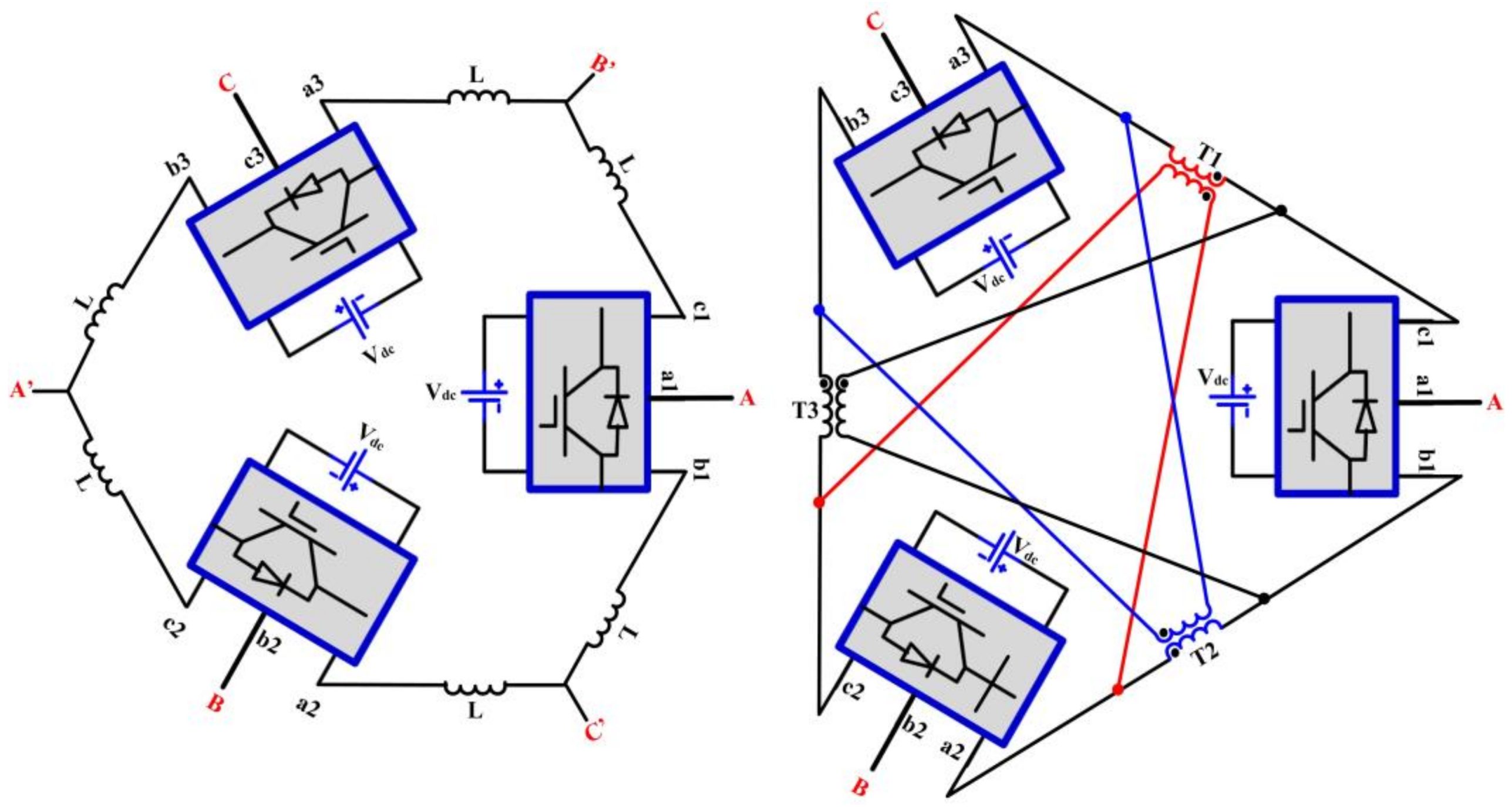
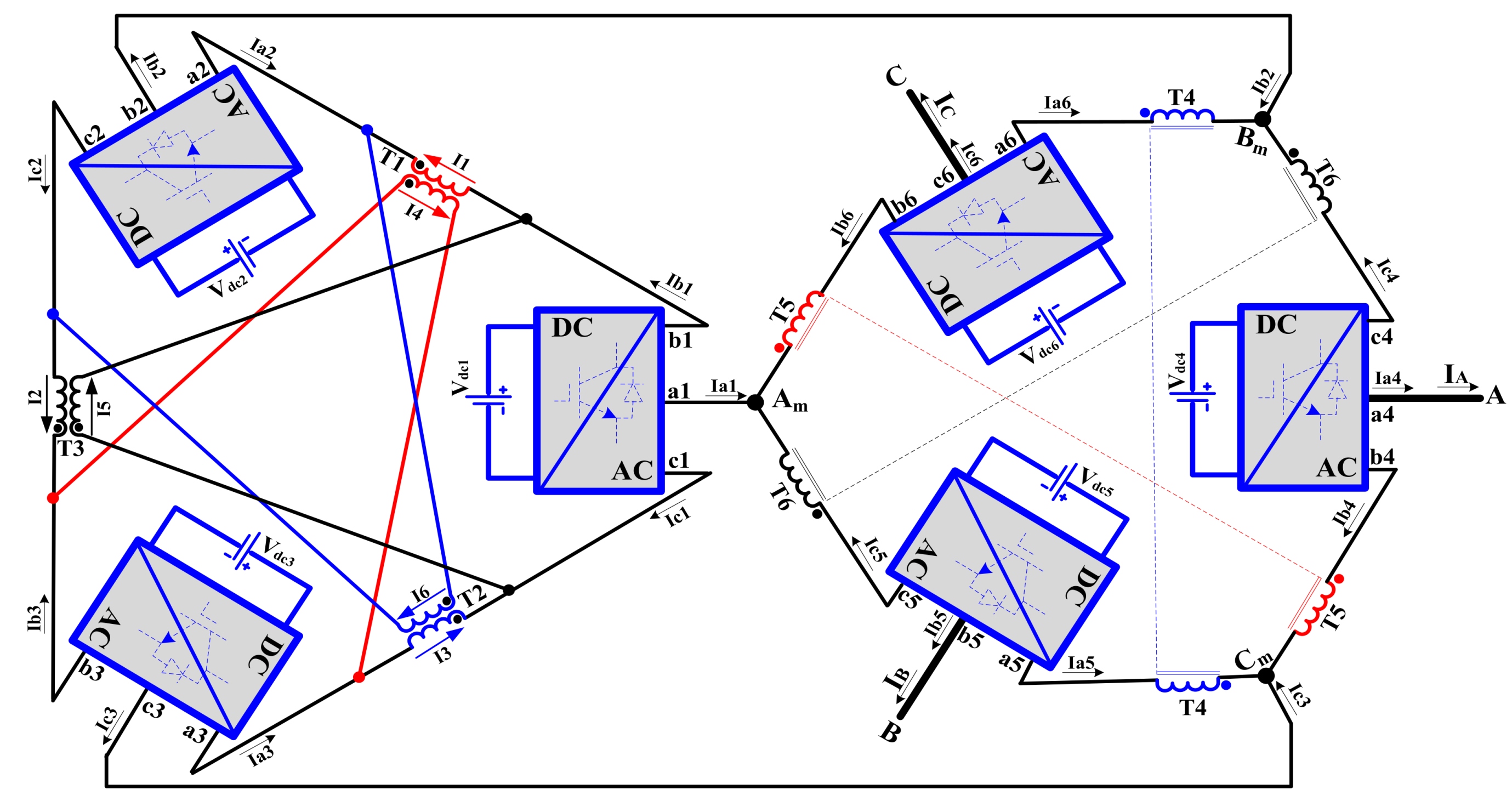
The proposed configuration of the three-phase grid-connected applications is shown in
Figure 2. This configuration is composed of six traditional two-level, three-phase VSC modules that have hexagonal interconnections to produce higher voltage levels, as shown in
Figure 2. Each VSC module supplies 1/6 of the converter’s output power.
The output terminal nodes of the proposed converter are labeled A (AC terminal node
a4 of module 4), B (AC terminal node
b5 of module 5) and C (AC terminal node
c6 of module 6). The other two AC terminal nodes,
b4 of module 4 and
a5 of module 5, are coupled with AC terminal node
c3 of module 3 by way of magnetic element. AC terminal nodes
c4 of module 4 and
a6 of module 6 are coupled by way of a magnetic element with AC terminal node
b2 of module 2. Similarly, AC terminal nodes
c5 of module 5 and
b6 of module 6 are coupled with AC terminal node
a1 of module 1 via a magnetic element. The remaining two AC terminals of each module are connected to adjacent modules through another magnetic element (e.g.,
T1,
T2 and
T3 for modules 1, 2 and 3, respectively). AC terminal
b1 of module 1 is coupled to AC terminal
a3 of module 3 through the primary winding of
T1; AC terminal
c1 of module 1 is coupled to AC terminal
a2 of module 2 through the primary winding of
T2. The remaining modules consist of similar connections, as shown in
Figure 2.
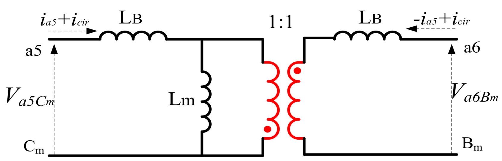
4. The Role of the Magnetic Elements
This section investigates the function of the magnetic elements within the proposed converter. Two inductors with an equal number of turns are coupled together; that is, an input to one side produces an output on both sides, as shown in
Figure 3. As the turn ratio is approximately 1:1, the self-inductances of the primary and secondary windings are the same (e.g.,
). The two-winding magnetic element
T4 is selected for analysis. Applying the voltage relationships from two-winding transformers results in the following equations:
where
,
,
and
, such that
is the leakage inductance (which is expected to be identical for all windings) and
is the magnetizing inductance.
It is obvious from
Figure 3 that the voltage drop on one of the magnetic elements is
Using (17) and (18), the voltage across the coupled inductor can be expressed as
Therefore, the total voltage drop across the magnetic elements can be expressed as
The magnetizing inductance is much higher than the leakage inductance. Therefore, neglecting the leakage inductance, the two-winding magnetic element imposes twelve times the magnetizing inductance for the circulating current.
6. Simulation Results
The proposed converter can be implemented using various VSCs with six isolated DC links. The two-level VSC topology is chosen for implementing the present topology because of its simplicity. To confirm the theoretical analysis provided in
Section 3, simulations are carried out in the MATLAB/Simulink environment. The DC-link voltage is 30 V. The output terminals of the converter are connected to an inductive load of 77 mH, connected in a wye configuration.
The thirteen-level line-line voltages of the proposed converter (for a modulation index of 1.0 and a switching frequency of 900 Hz) are generated in a steady state, as shown in
Figure 5. The voltages are balanced, as demonstrated in (15). It is clear from
Figure 5 that the voltage across the load terminals is multistep and, therefore, has low
dv/
dt and low harmonic content.
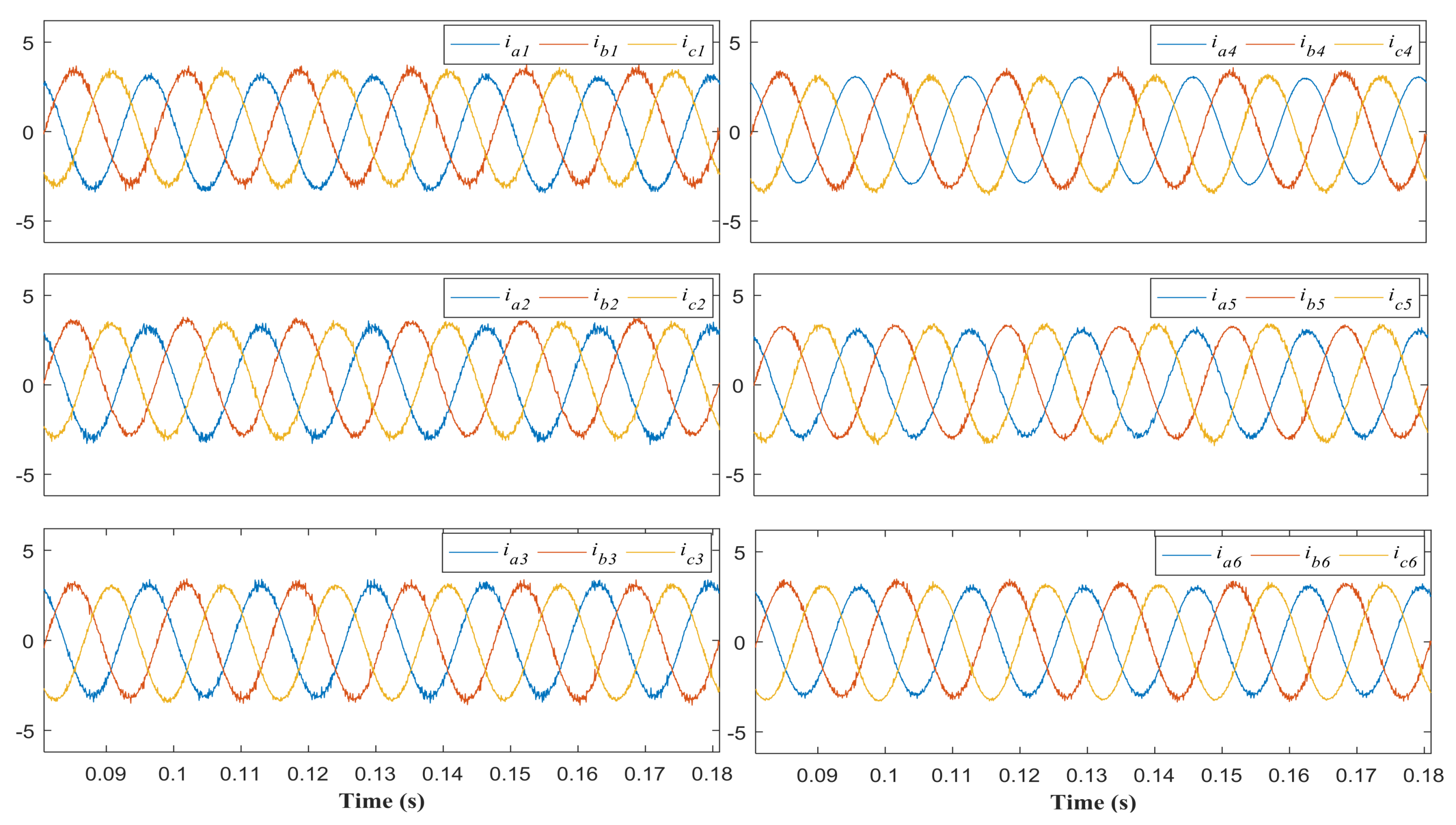
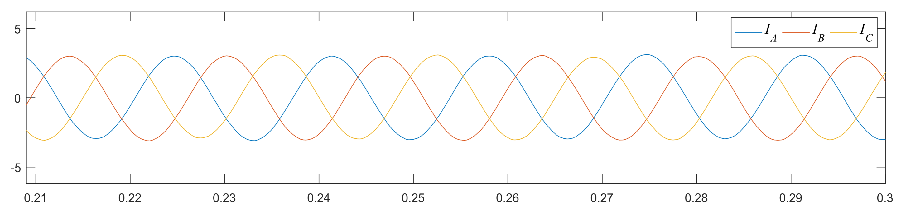
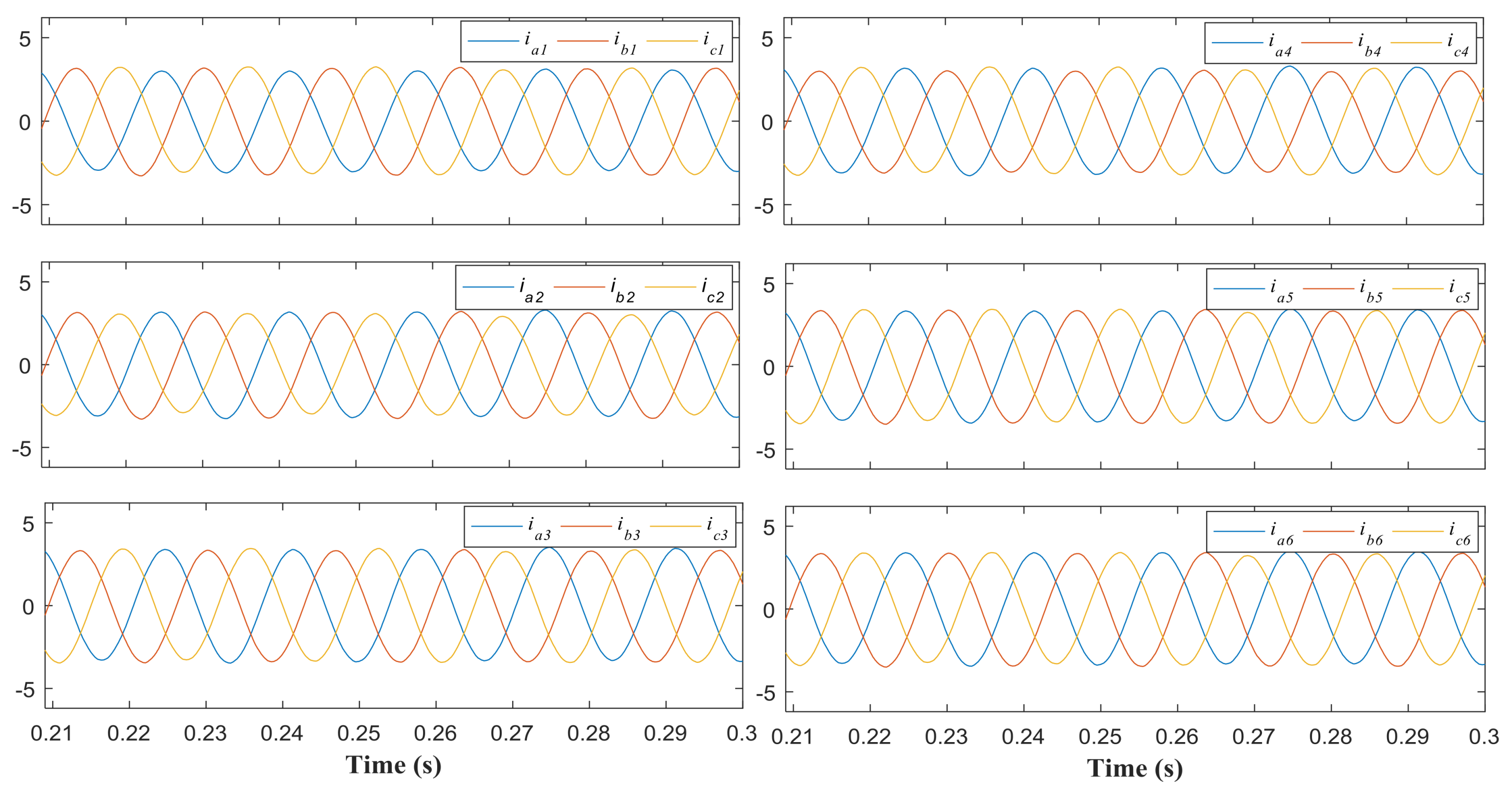
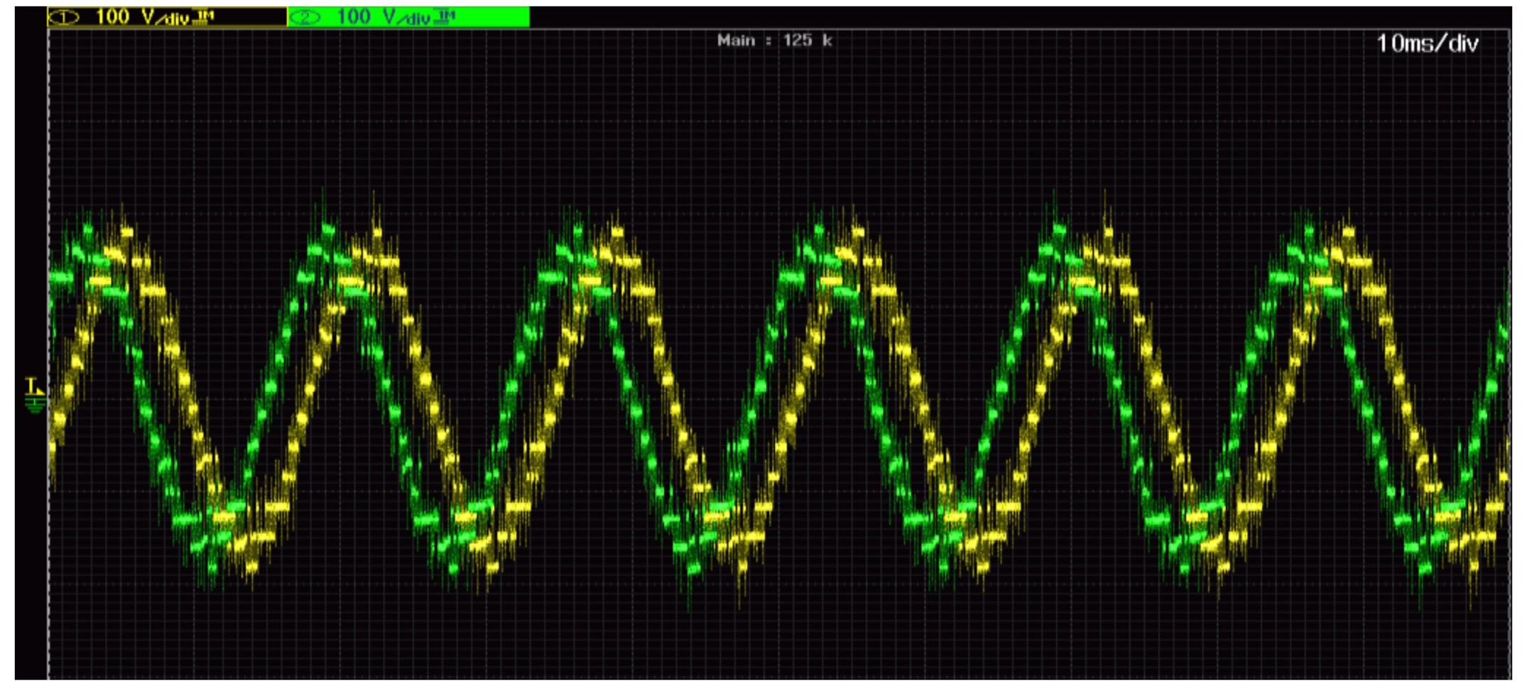
Figure 6 and
Figure 7 show the currents of the VSC modules. Given the configuration of the three-phase converter, the line currents of every VSC module within the converter are symmetrical, thus verifying the relationship in (9). Moreover, the currents inside every VSC module are the same as the output current.
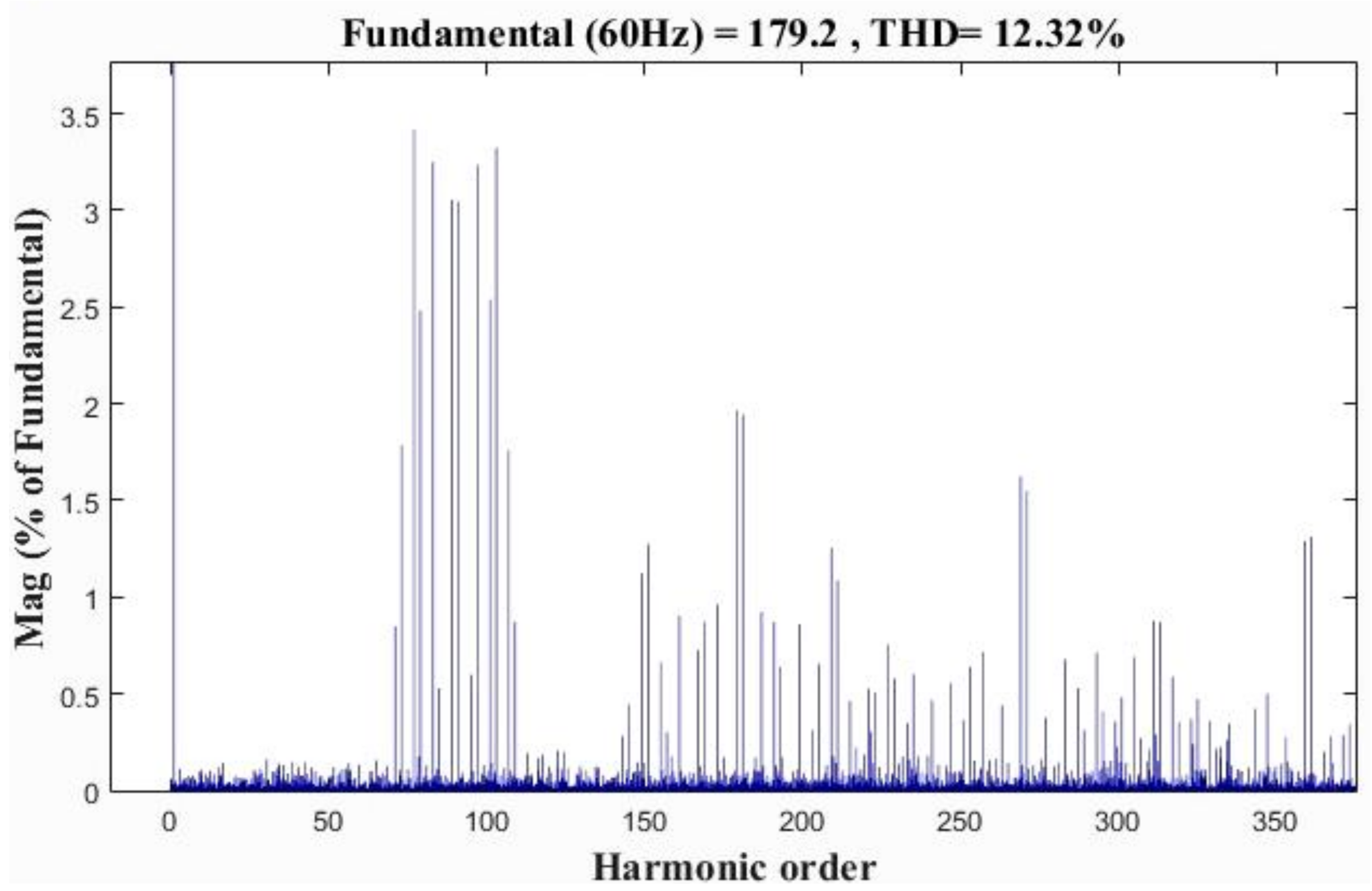
A third order harmonic with an amplitude of 1/6 with respect to the fundamental component is injected in order to increase the amplitude of the fundamental output voltage by about 15% without over modulation. A comparative analysis between the line-line voltages based conventional PWM and third harmonics injection PWM (THI-PWM) is shown in
Figure 8. It can be observed from
Figure 8 that the magnitude of the low order harmonics has been considerably reduced to a negligible value. The total harmonic distortion (THD) of the output line voltage is 12.32%. Because of the 120 phase shifts among VSC converters, all triplen harmonics in line voltages are also very small. Moreover, the first center band harmonics are cancel and shifted to 90 times of fundamental frequency by providing a phase shift of 120 between carrier waves. Consequently, the effective switching frequency of the line-line voltage is six times higher than the switching frequency.
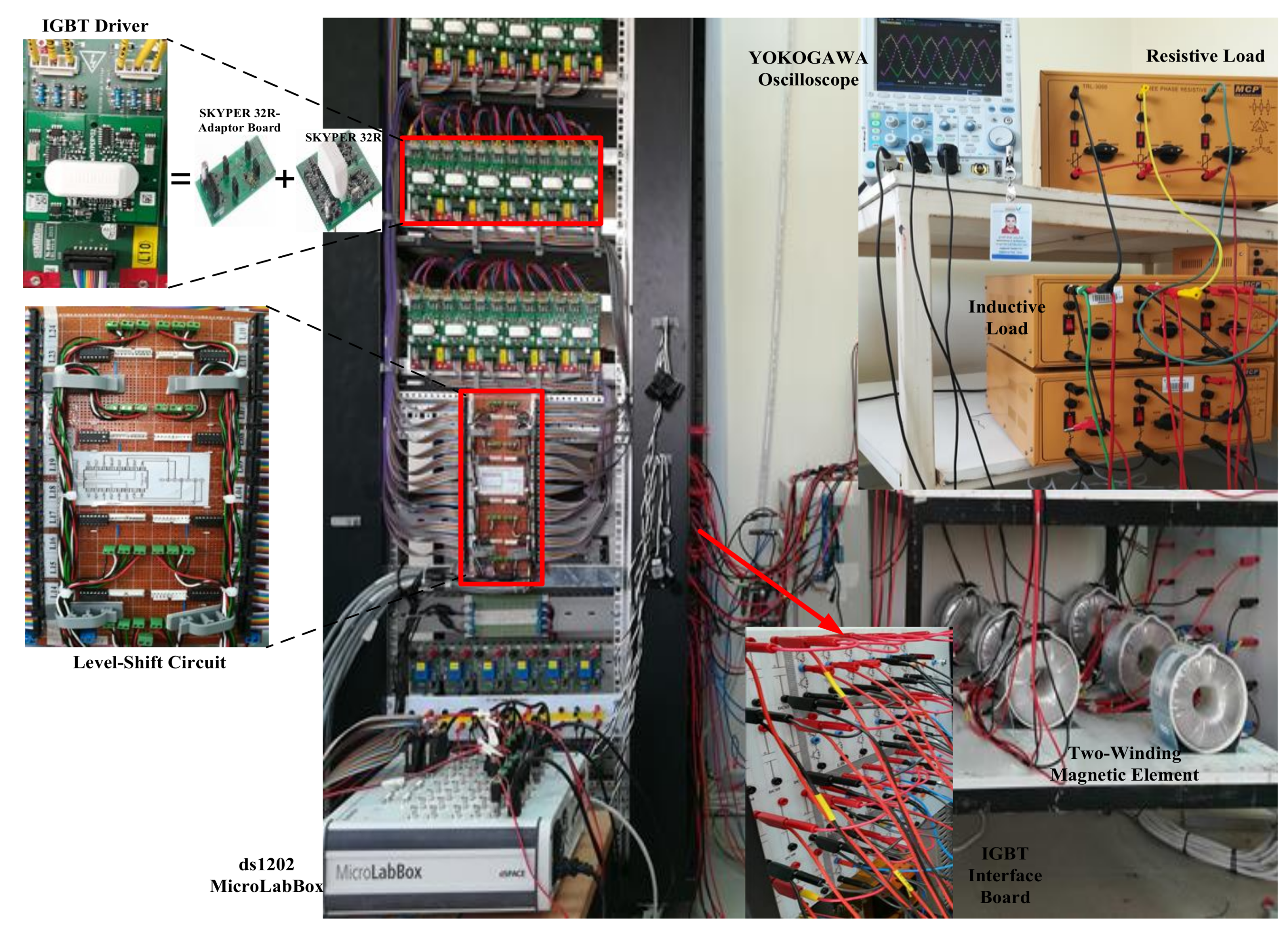
7. Experimental Results
An experimental prototype of the proposed converter is built to the following specifications:
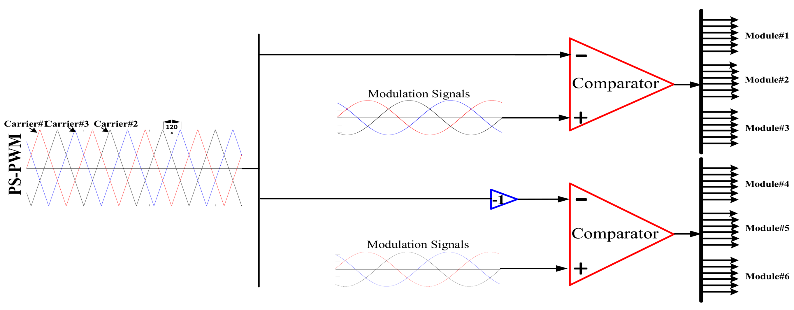
To validate the proposed converter’s good performance, the PS-PWM technique shown in
Figure 4 is implemented using a ds1202 MicroLabBox. The fundamental frequency of the reference signal is 60 Hz and the switching frequency is 900 Hz.
Figure 9 shows a prototype of the proposed converter. It includes six magnetic elements; 6 two-level, three-phase VSC modules; resistive-inductive loads; and the ds1202-based controller. The block diagram of the PWM control system is shown in
Figure 4. The gating signals generated in the ds1202 controller are applied to the IGBT via an isolated driver. In the prototype, SKM75GB12V IGBTs (ratings: 1200 V and 75 A) are used as switching devices. The gate driver SKYPER 32R provides both amplification and isolation from the power circuit. An oscilloscope (YOKOGAWA model no. DLM2054) is used to measure the output voltages. The line currents are measured using a Hall effect current sensor (model no. LTS 25-NP). The currents measured using this sensor are applied to the ADC of the ds1202 board and the resulting measured signals are drawn using the Simulink environment. The experimental parameters are shown in
Table 1.
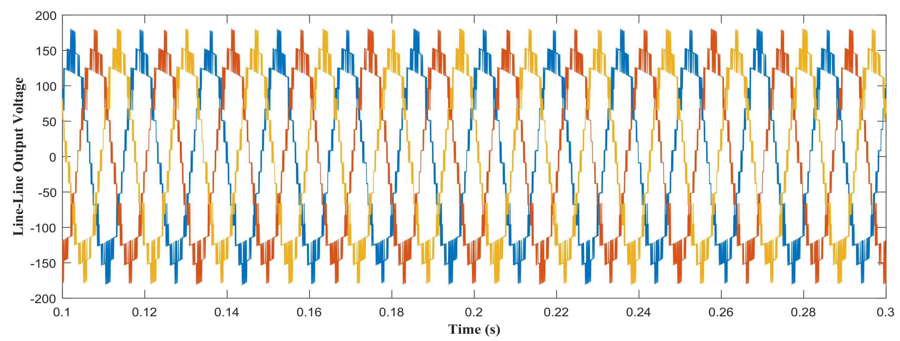
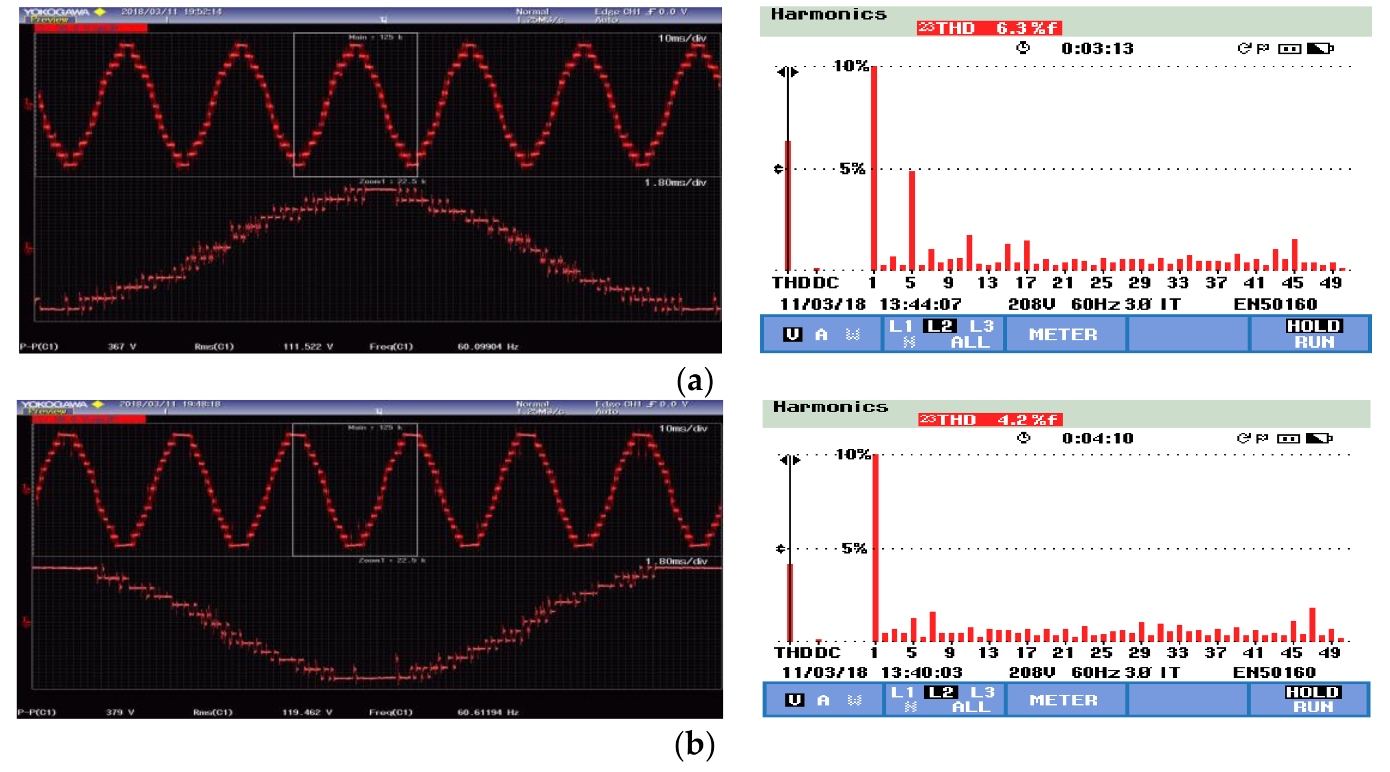
Figure 10 and
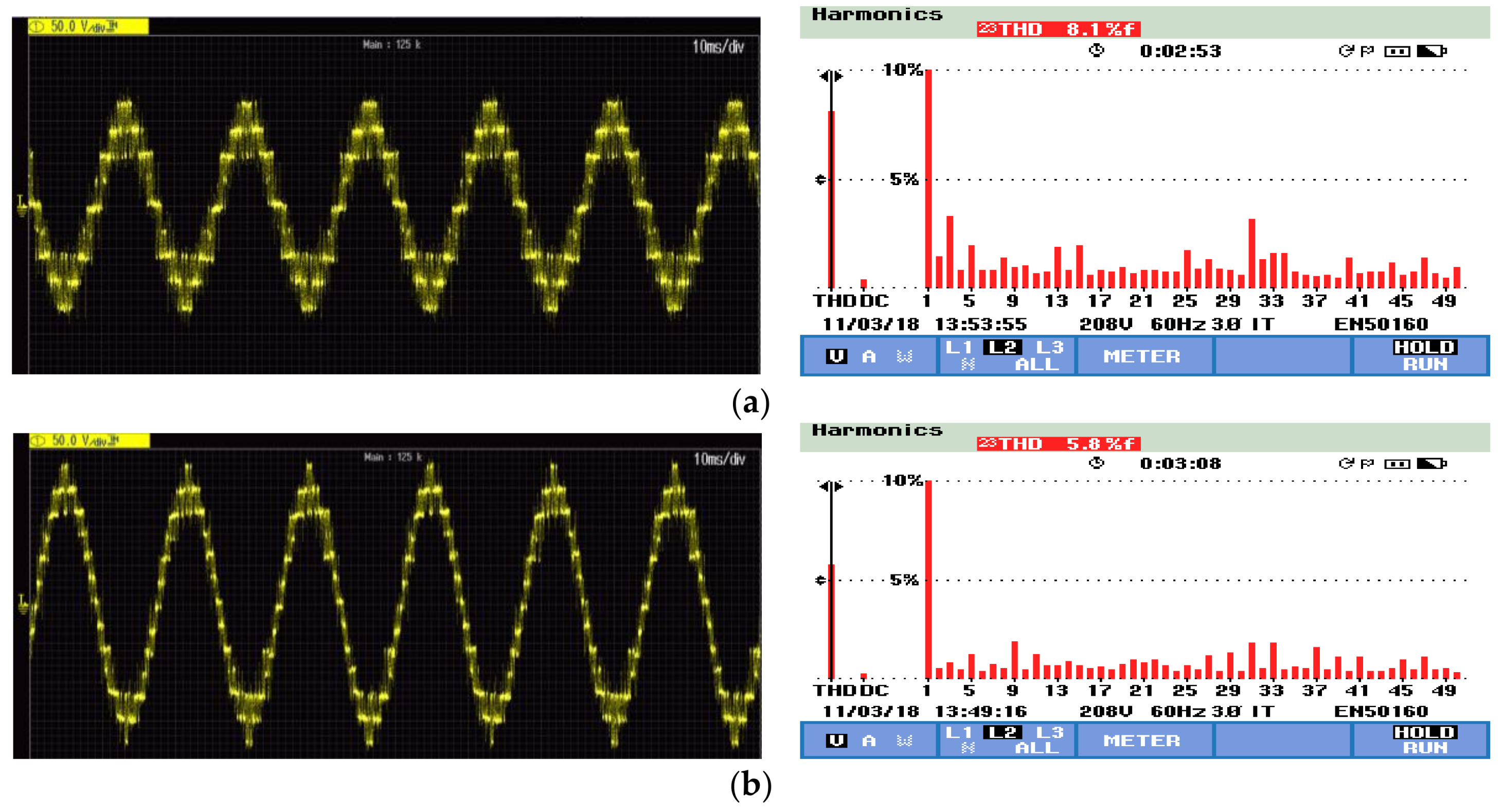
Figure 11 show the line-line voltage waveforms and fast fourier transform (FFT) results for a wye-connected resistive load (48 Ω) at different modulation index. The figures show that for both cases, a poor THD are obtained when the converter operated at low modulation index. This is to be expected because at low modulation index, the converter essentially behaves like a conventional seven-level converter. A better THD is obtained when the converter operated at higher modulation index. Moreover, it can be seen from the results that the increase in the index of modulation rejects the first harmonics' non-null worms of the higher frequencies and thus facilitates filtering. A comparative analysis between the line-line voltages based conventional PWM and third harmonics injection PWM (THI-PWM) is shown in
Figure 11. It can be observed that the magnitude of the low order harmonics has been considerably reduced to a negligible value. The results also show that the injection of harmonic 3 in the reference signal makes it possible to improve the form of the output voltage and to increase the maximum amplitude of fundamental in the output voltage. Besides, the analysis of the results shows that the spectrum of harmonics of the output voltage is improved compared to the triangular sinusoidal PWM.
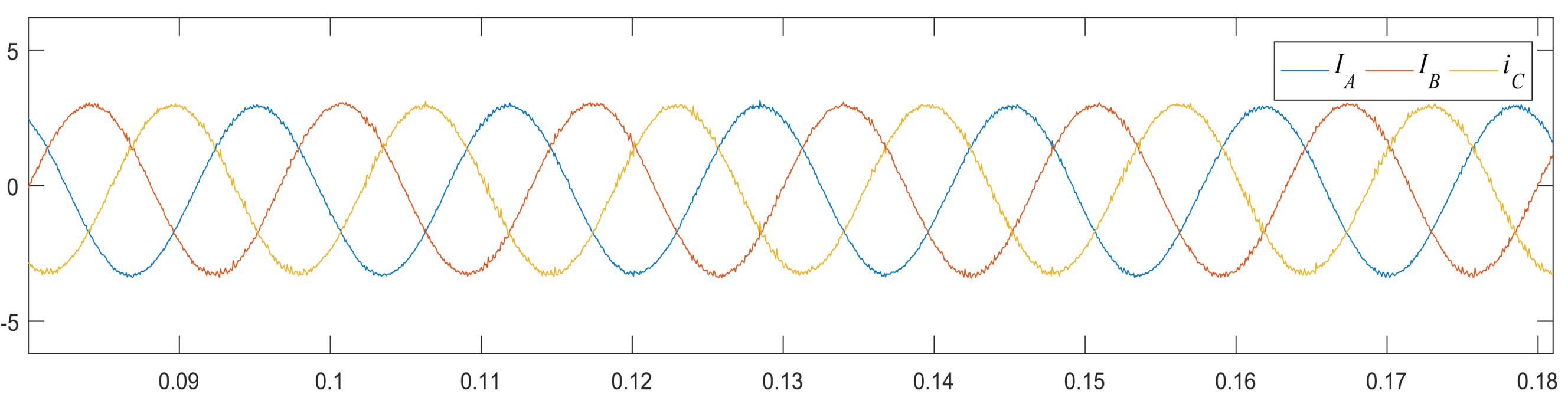
The steady-state experimental results of the proposed converter are presented in
Figure 12,
Figure 13 and
Figure 14. The output terminals of the converter are connected to an inductive and resistive load of 48 Ω resistance and 77 mH inductance and connected in a wye configuration. The thirteen-level line-line voltages of the proposed converter (with a modulation index of 0.95 and a switching frequency of 900 Hz) are shown in
Figure 12. As shown in
Figure 13 and
Figure 14, the line currents of every VSC module within the converter are symmetrical and are the same as the output current, hence verifying the relationships in (9) and the simulation results in
Figure 7.
The proposed converter was proposed to generate 13 output voltage levels. If we want to synthesize the same number of output voltage levels with conventional multilevel converters, we can find that they need many components compared with the proposed scheme as given in
Table 2. As shown in this table, the proposed topology has the least number of switches compared to the prior art topologies (e.g., NPC, FC, CHB).
8. Conclusions
This paper introduces an isolated, cascaded, multilevel VSC topology employing two-winding magnetic elements for high-power applications. The topology consists of 6 two-level, three-phase VSCs with isolated DC links and 6 two-winding magnetic elements. The structure of the proposed topology is given and analyzed in detail, including the voltage relationships, current relationship, power allocation and the modulation of PS-PWM. The power capability of the proposed VSC is six times higher than that of each VSC module. Each VSC contributes equally to the total power without the need for a sharing algorithm; thus, the converter operates as a single, three-phase VSC. The comparative analysis with classical NPC, FC ad CHB shows superior features of less IGBTs, capacitor requirement and less diodes. It reduces the IGBTs count by 50% and isolated energy sources requirement by 33.3% compared with a three-phase CHB topology. To confirm the performance of the proposed topology, it is simulated in the MATLAB/Simulink environment; the results are also experimentally demonstrated using a laboratory prototype.

 ,
, 


