Hardware in the Loop Real-time Simulation for the Associated Discrete Circuit Modeling Optimization Method of Power Converters

Department of Electrical Engineering, Beijing Jiaotong University, Beijing 100044, China
*
Author to whom correspondence should be addressed.
Energies 2018, 11(11), 3237; https://doi.org/10.3390/en11113237
Submission received: 22 October 2018
/
Revised: 13 November 2018
/
Accepted: 19 November 2018
/
Published: 21 November 2018
Abstract
:Due to the complicated circuit topology and high switching frequency, field-programmable gate arrays (FPGA) can stand up to the challenges for the hardware in the loop (HIL) real-time simulation of power electronics converters. The Associated Discrete Circuit (ADC) modeling method, which has a fixed admittance matrix, greatly reduces the computation cost for FPGA. However, the oscillations introduced by the switch-equivalent model reduces the simulation accuracy. In this paper, firstly, a novel algorithm is proposed to determine the optimal discrete-time switch admittance parameter, Gs, which is obtained by minimizing the switching loss. Secondly, the FPGA resource optimization method, in which the simulation time step, bit-length, and model precision are taken into consideration, is presented when the power electronics converter is implemented in FPGA. Finally, the above method is validated on the topology of a three-phase inverter with LC filters. The HIL simulation and practicality experiments verify the effect of FPGA resource optimization and the validity of the ADC modeling method, respectively.
1. Introduction
Hardware in the loop (HIL) real-time simulation of power electronics converters on field-programmable gate arrays (FPGA) has gained more attractiveness because it can meet challenges [1,2,3] relating to the more complex topology of power electronics converters and achieve a higher switching frequency, etc. [4,5,6,7,8]. However, the modeling method of power electronics converters is a challenging task due to the changing topology of the circuit [9,10,11]. Modified nodal analysis (MNA) and the state-space approach require elaborate identification of all possible circuit states of power electronics converters, which can hardly be realized in real-time simulation [12,13,14]. The Voltage-Controlled Current Source (VCCS) modeling method could obtain a precise switching state [15], but it needs the additional iterative numerical solution, which will increase the amount of calculation. The associate discrete circuit (ADC) modeling method presented by Pejovic [16,17], has a fixed admittance matrix by selecting the appropriate switch admittance parameter, Gs, which increases the simulation efficiency.
However, the switch representation of the ADC modeling method introduces artificial transients [3], which causes additional loss compared to the ideal switching model. Some solutions to suppress oscillation error have been proposed. In particular, a damping resistance can be added in series to the discrete-time switch model [18]. However, this approach increases the model complexity as well as poses the problem regarding the optimum selection of the value of the damping resistance. Another more general method to solve this problem is to select the optimal switch admittance parameter, Gs. One possibility is to consider a priori the switch admittance parameter, and then find the corresponding optimum value by comparing the offline simulation results with the benchmark results to minimize the relative errors; however, such a trial-and-error method has a low efficiency [19]. Within this context, the paper proposes a novel approach to choose the optimal switch admittance parameter, Gs, by minimizing the switching loss to reduce the computations required and increase the simulation precision.
The high parallelism offered by FPGAs and their potential to conduct a real-time simulation in the nanosecond range make these devices an emerging processor for real-time simulation of a complex power electronic system [20,21,22,23,24]. However, due to the limited FPGA hardware resources, it is especially important to balance FPGA resource consumption and simulation accuracy. Theoretically, precise simulation results could be obtained by excessive bit-length, but it would cause unnecessary FPGA resource consumption [25,26]. Meanwhile, with the purpose of decreasing the discretization process error, the simulation time step should be set as small as possible; however, the quantization error caused by a small simulation time step may reduce the simulation accuracy [27]. Some scholars conducted a related qualitative analysis respectively but lacked overall quantitative calculations. Therefore, how to precisely select the bit-length and simulation time step is a valuable task that needs to be solved in the realm of HIL real-time simulation in FPGA. Additionally, High-Level Synthesis tools such as, Vivado High Level Synthesis (VHLS) and OpenCL SDK [28,29], allow the use of high-level languages to ease the burden of design and verification of hardware, which reduces the development time and difficulty and improves the economy and efficiency [30,31,32,33].
The remainder of the paper is organized as follows. First, Section 2 presents a minimum switching loss method to select the optimal discrete-time switch admittance parameter. The proposed method is verified by three-phase inverter offline simulation in Section 3. Next, Section 4 presents a quantitative algorithm to choose the minimum time step and bit-length that meet the model precision to minimize the FPGA resources consumption. Section 5 compares and verifies the VHLS-based HIL real-time simulation results and practicality experiment results of the three-phase inverter. The discussion is in Section 6. Finally, Section 7 gives the conclusion of this paper.
2. Associated Discrete Circuit Modeling Optimization Method
2.1. Associated Discrete Circuit Modeling Method
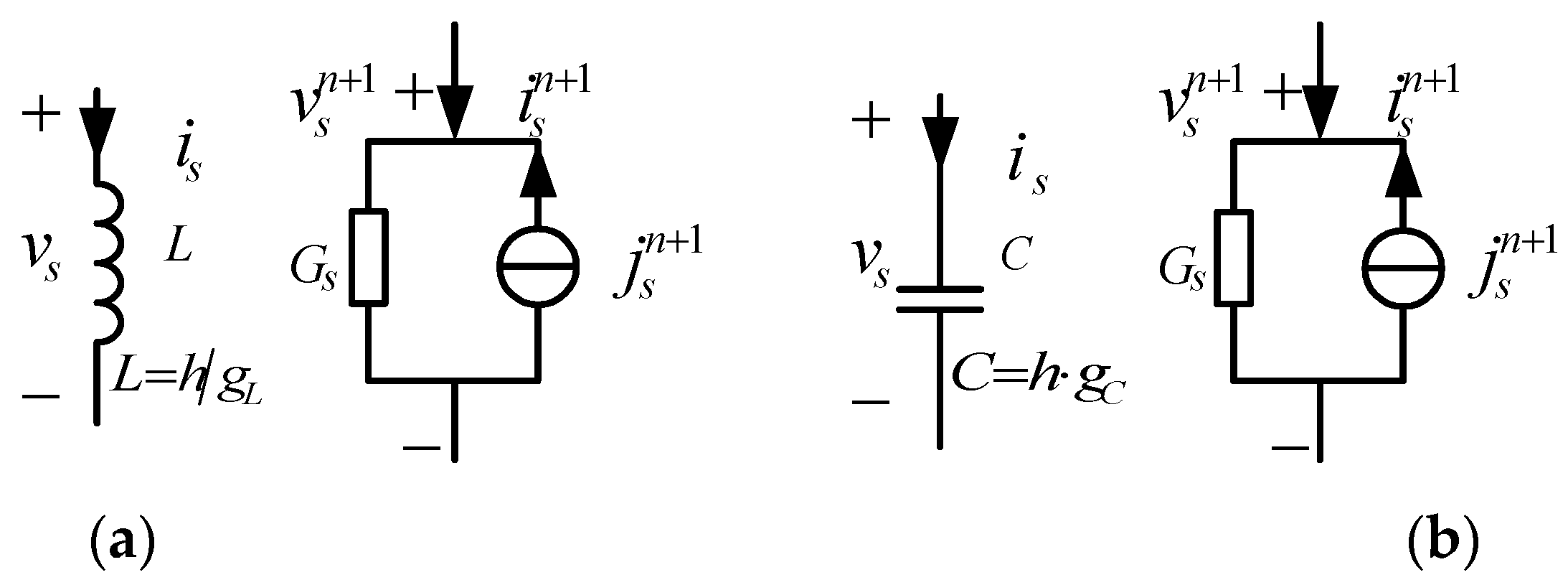
The modified nodal analysis (MNA) proceeded using assembling network equations after discretizing all circuit devices using the backward Euler method (BEM). The companion circuit of a dipole device is a discrete Norton equivalent given by:
where geq is the Norton equivalent admittance associated with the dipole, in+1 is current traversing the dipole, jn+1 is the history term of the current traversing the dipole, and vn+1 is the voltage drop at its terminals.
For equivalent admittance of a capacitance C,
where h is simulation time step. With all circuit components represented by their companion circuit, it is possible to set the system of equations Hxn+1=bn, where H is the fixed admittance matrix, xn+1 is the vector of unknown nodal voltages, and bn is the vector of known current injections including independent sources and its history terms.
The ADC switch model is shown in Figure 1, the switch is modeled as an inductance L or capacitance C depending on its ON/OFF status. The values of L and C can be calculated from Equations (2) and (3). Both switch states can be equivalent to the parallel of the switch admittance parameter Gs and switching current history term .
By imposing Gs=gC=gL in the ADC switch model, system matrix H becomes time-invariant regardless of the switching status. Compared to an ideal switch model, which has zero resistance and zero voltage drop during the ON state, and switches between ON/OFF in instantly, The ADC switch model has transient errors. From Figure 1, one way to increase the simulation accuracy is to reduce the time step h, which is limited by two factors: (1) the minimum time step h is strictly limited by the FPGA computation performance; (2) when h is too small, it will lead to the quantization error, which increases the simulation error. Moreover, the switch admittance parameter, Gs, has an important influence on the model precision; therefore, another way is choosing its optimal value for the simulation.
2.2. The Switch Admittance Parameter Gs Value for Minimum Switching Loss
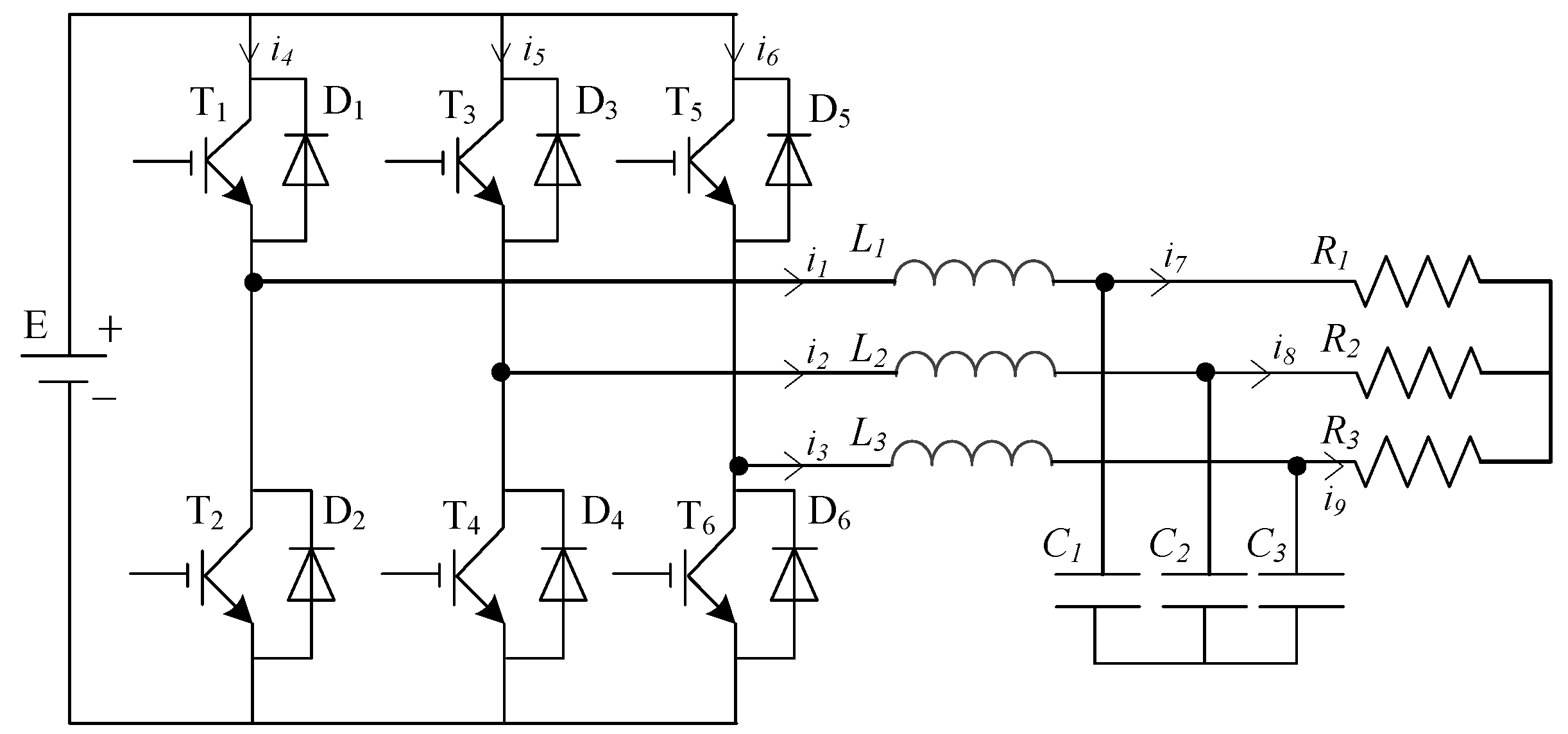
The three-phase inverter with LC filter, shown in Figure 2, is as an illustration to select the optimal Gs value for minimum switching loss.
In Figure 2, T1~T6 are Insulated Gate Bipolar Transistors (IGBTs), Li (i = 1, 2, 3) is the grid-side inductance, Ci (i = 1, 2, 3) is the filter capacitor, i1–i3 are the phase current of the output, and i7–i9 are the load current.
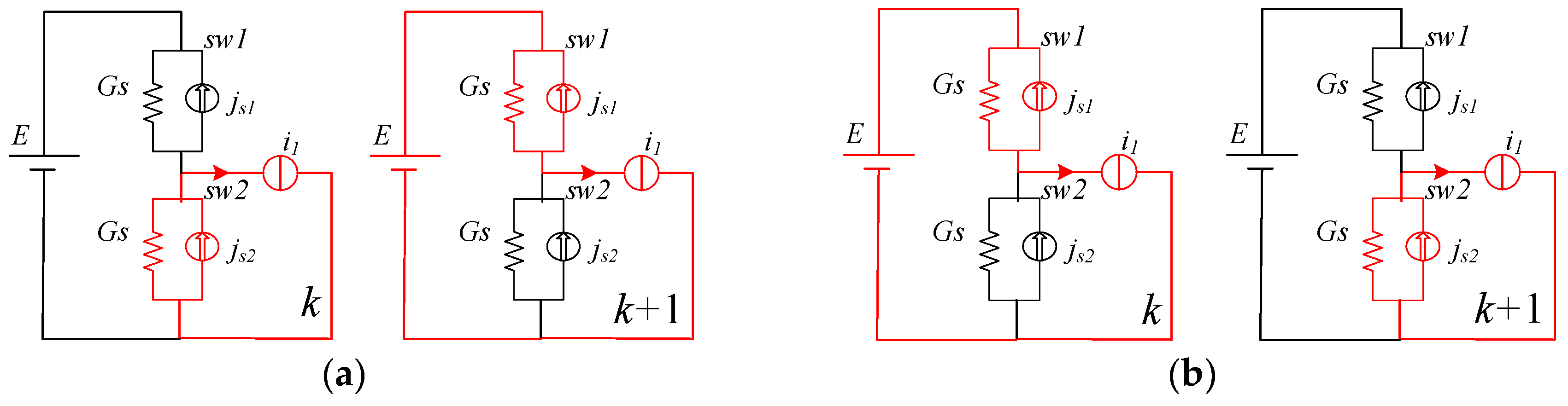
When modeling the inverter, the load can be equivalent to the current source by the substitution theorem. The commutation process of sw1 in one inverter arm is shown in Figure 3, in which sw1 and sw2 indicate the upper and lower switching devices of the inverter arm.
In Figure 3a, it is assumed that at the k step, the upper switch sw1 is in the OFF state. In this case, the switch is equivalent to the C, and the energy stored from the C can be calculated by the following equations. The energy stored in the C exists in the form of a parallel current source.
In the k + 1 step, the switch sw1 is turned ON and is equivalent to the L, which is known from Equation (3):
It can be seen from Equations (6)–(8) that the energy stored on the equivalent capacitance disappears during the OFF-ON commutation process of the top switch, sw1.
Similarly, in Figure 3b, it is also assumed that at the k step, the upper switch sw1 is in the ON state. In this case, the switch is equivalent to the L, and the energy stored on the L can be calculated by the following equations. The energy stored on the L exists in the form of a parallel current source.
In the k + 1 step, the switch sw1 is turned OFF and is equivalent to the C, which is known from Equation (2), so
It can be seen from Equations (11)–(13) that the energy stored as equivalent inductance disappears during the ON-OFF commutation process of the top switch, sw1.
Therefore, the energy always disappears at the moment of turning-ON and turning-OFF, and the total switching losses can be calculated in Equation (14), in which m and n are the total switching times of turning-ON and -OFF:
To minimize the switching loss, the optimal Gs can be calculated via the following equation,
For most power electronics converters, the switch current isw(kj) and voltage vsw(ki) are equal to the load current iload(kj) when it is in the ON state and Direct Current (DC) voltage, Vdc, when it is in the OFF state, respectively, and the total switching times of turning-ON and turning-OFF are equal. Therefore, the optimal Gs can be expressed as,
For the three-phase inverter depicted in Figure 2, supposing the switching frequency is sufficiently higher than the load fundamental modulation frequency, the optimal Gs can be calculated using Equation (18), in which Io is the Root Mean Square (RMS) value of load current. Moreover, for the DC-DC circuit, the load current RMS value, Io, is treated as the average value of the load current.
It should be noticed that the optimal Gs value depends on the ratio between the load current RMS value and the DC voltage, which varies with the dynamic load. This method is only valid for the specific working point of the power converters, which is also the main drawback of the ADC modeling method.
3. Simulation Verification
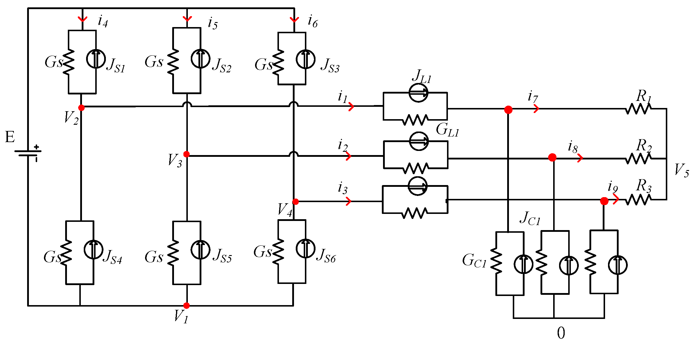
The equivalent model of the three-phase inverter using the ADC method is shown in Figure 4, and the system parameters are shown in Table 1.
Firstly, the switching current and voltage are estimated, and the optimal Gs is solved:
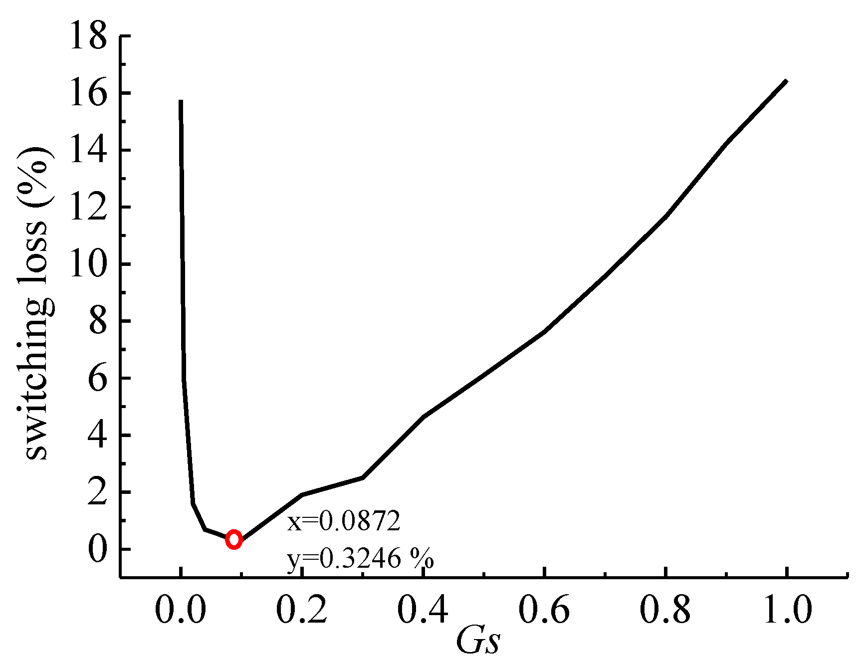
To verify that Equation (19) is the optimal admittance parameter with the minimum switching loss, the Gs is in the range of 0.01 to 1, and the trend chart of the switching loss with the Gs is obtained as shown in Figure 5. It can be seen that the total switching loss is minimum at the point Gs = 0.0872, which verifies the correctness of Equation (19).
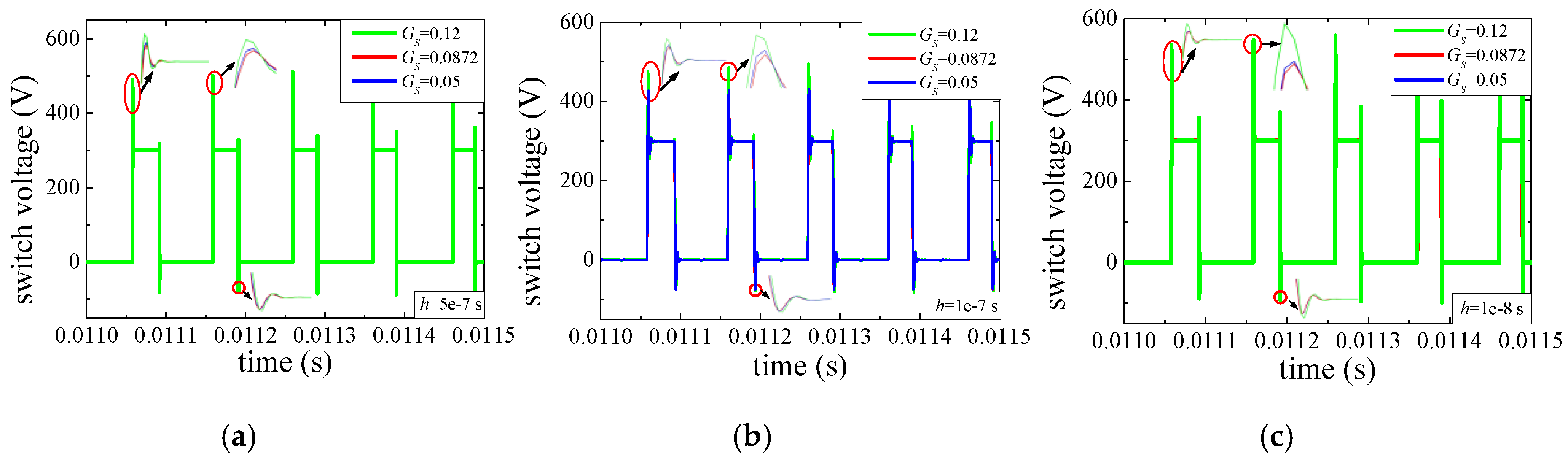
In order to further analyze the influence of Gs on the switching loss, three typical simulation results are compared, which are the optimal Gs, the smaller Gs (0.05), and the larger Gs (0.12). We can see from Equations (16) and (17) that the choice of optimal Gs is independent of the time step, h. Comparing these three Gs values under three different time steps (h = 1e–8 s, 5e–7 s, 1e–7 s), the switching voltage waveform comparison is shown in Figure 6. We can verify that the optimal Gs oscillation is the smallest and the convergence speed is the fastest no matter what the time step is. Section 4 explains the reason why the overall switch voltage error is the smallest when the time step h is 1e-7 s.
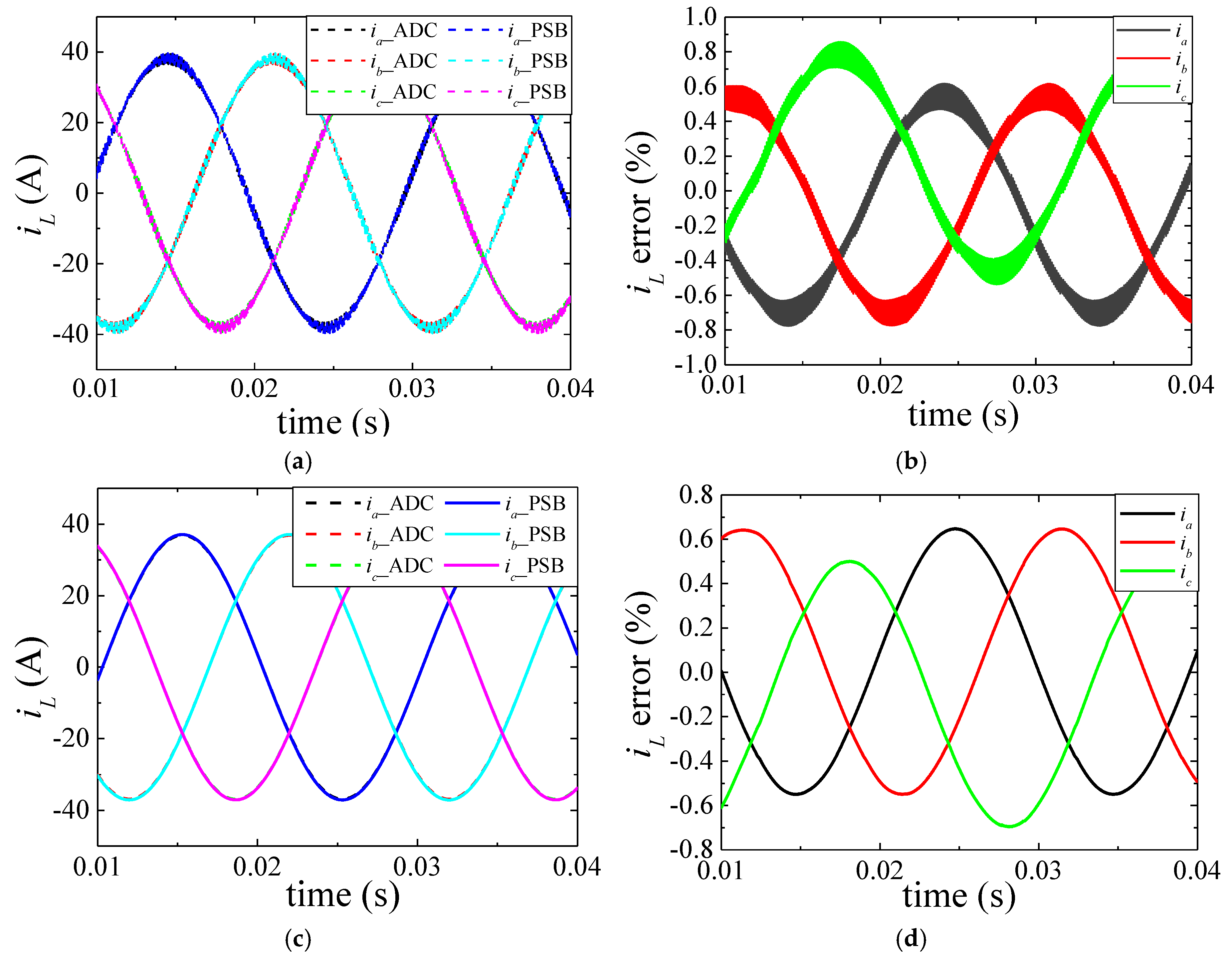
In Figure 7, the Matlab/Power System Blockset (PSB) is used as the benchmark of the simulation results. We can see the simulation waveform’s comparison of ADC modeling and PSB modules of the three-phase inverter, and the relative errors are less than 1%. Although there are transient peaks when the switch state changes, the simulation precision can be guaranteed by selecting the optimal Gs.
4. FPGA Implementation
In the process of HIL real-time simulation for power electronics converters, due to the limited FPGA resources, the minimum bit-length that meets the model precision requirement needs to be chosen to optimize the FPGA resource. Regarding the time step, although a small step can reduce the truncation error caused by discretization, it will increase calculation times and the quantization error. Therefore, the quantitative algorithm of bit-length, time step, and simulation precision has an important significance on FPGA implementation of HIL real-time simulation.
4.1. FPGA Resource Optimization Method
To accurately describe the relationship between simulation precision and model quantization error [25,26], the concept of signal-to-noise ratio (SNR) is used with average value and variance of the signal x and average value and variance of the quantization error e.
The key problem of calculating the SNR is to solve the quantization error that includes the quantization error of the signal and coefficient and the quantization error in the multiplication operation. Taking the rounding quantization for example, this paper describes the total (rounding) quantization error in detail.
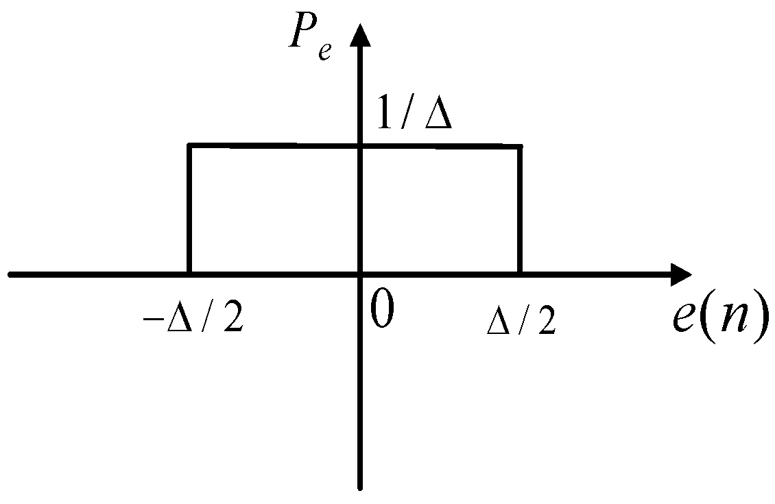
To calculate the statistical parameters of the quantization errors of the signal, it is equivalent to a noise sequence with white uniform equal probability distribution. The probability density distribution is shown in Figure 8.
For the quantization error, its statistical parameters are as follows:
The fixed-point operation includes addition and multiplication. The addition operation does not produce quantization error because the bit-length does not increase. However, the multiplication operation increases the bit-length, so we need to round the extra bit-length, which introduces the rounding quantization error.
It is assumed that these are n1 bit-length before rounding and n2 bit-length after rounding. The quantization error is an integer multiple of . Assuming all errors are equal, the average value, variance, and RMS of the output signal y are:
We assume that ec and ex are quantization errors of coefficient c and signal x respectively, and ey is the quantization error of the multiplication operation process, so the output result y is:
The total quantization error eges of the multiplication is:
After calculating the statistical parameters of eges, we can obtain the SNR using Equation (20).
In order to apply the SNR calculation to power electronic modeling, SNR calculation needs to be generalized to matrix operation. We assume that output vector is equal to the product of the coefficient matrix and input vector as follows:
The various quantization errors in the matrix are shown in (27), and the total quantization error is:
We can obtain the SNR with the following equation:
4.2. Simulation Verification
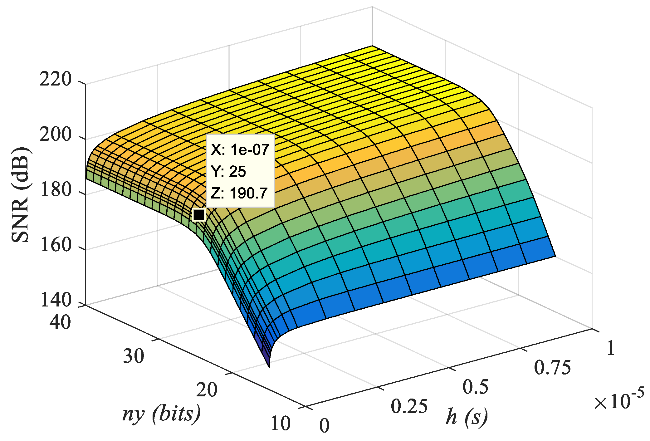
This paper applies the proposed SNR calculation method to the three-phase inverter, which obtains the quantitative relationship among bit-length ny, time step h, and model precision. The result represented by a surface plot is shown in Figure 9:
Figure 9 shows that when the bit-length ny increases to a certain bit, there is no longer a significant increase in the SNR, the higher bit-length just leads to unnecessary FPGA resource consumption. Meanwhile, the smaller the time step h is, the larger the rounding quantization error is. When time step h is less than 100 ns, the SNR reduces greatly, and the rounding quantization error plays a dominant role in the model precision. The optimal choices of time step h and bit-length ny are marked by the black dot in Figure 9, in which the time step h is determined by the highest third derivative of the SNR value with respect to h. The reason for this is that the point of the highest third derivative marks the most efficient time step h to reduce the rounding quantization error. The minimum ny is the optimal selection when the first derivative of the SNR value with respect to ny is equal to zero. The equation is shown:
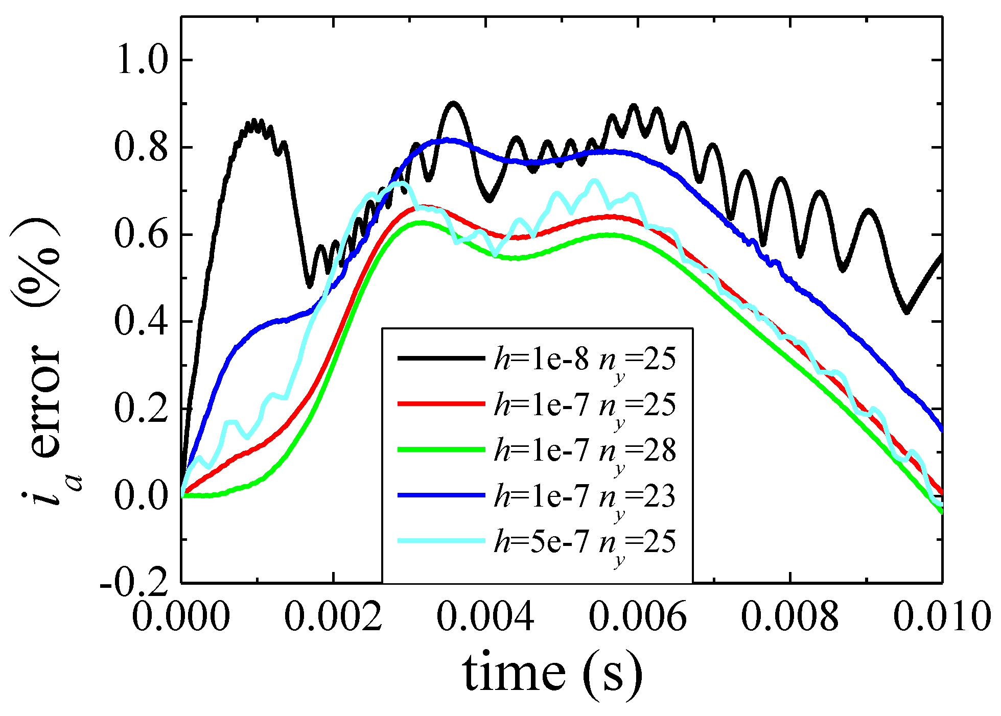
In order to demonstrate the validity of the chosen bit-length and time step in Figure 9, the simulation waveform of A phase current error comparison with different bit-lengths ny and time steps h is shown in Figure 10.
It is assumed that the optimal point (h = 1e–7 s, ny = 25 bits) is a reference point and four cases are considered, which are: (1) h = 1e–7, ny = 23; (2) h = 1e–7, ny = 28; (3) h = 1e–8, ny = 25; (4) h = 5e–7, ny = 25. It can be seen that when h is 1e-7, the model error for 28 bits is slightly larger than that for 25 bits, but both are less than 0.7%. In order to minimize the FPGA resource, 25 bits should be chosen. The offline simulation also verifies the quantitative algorithm.
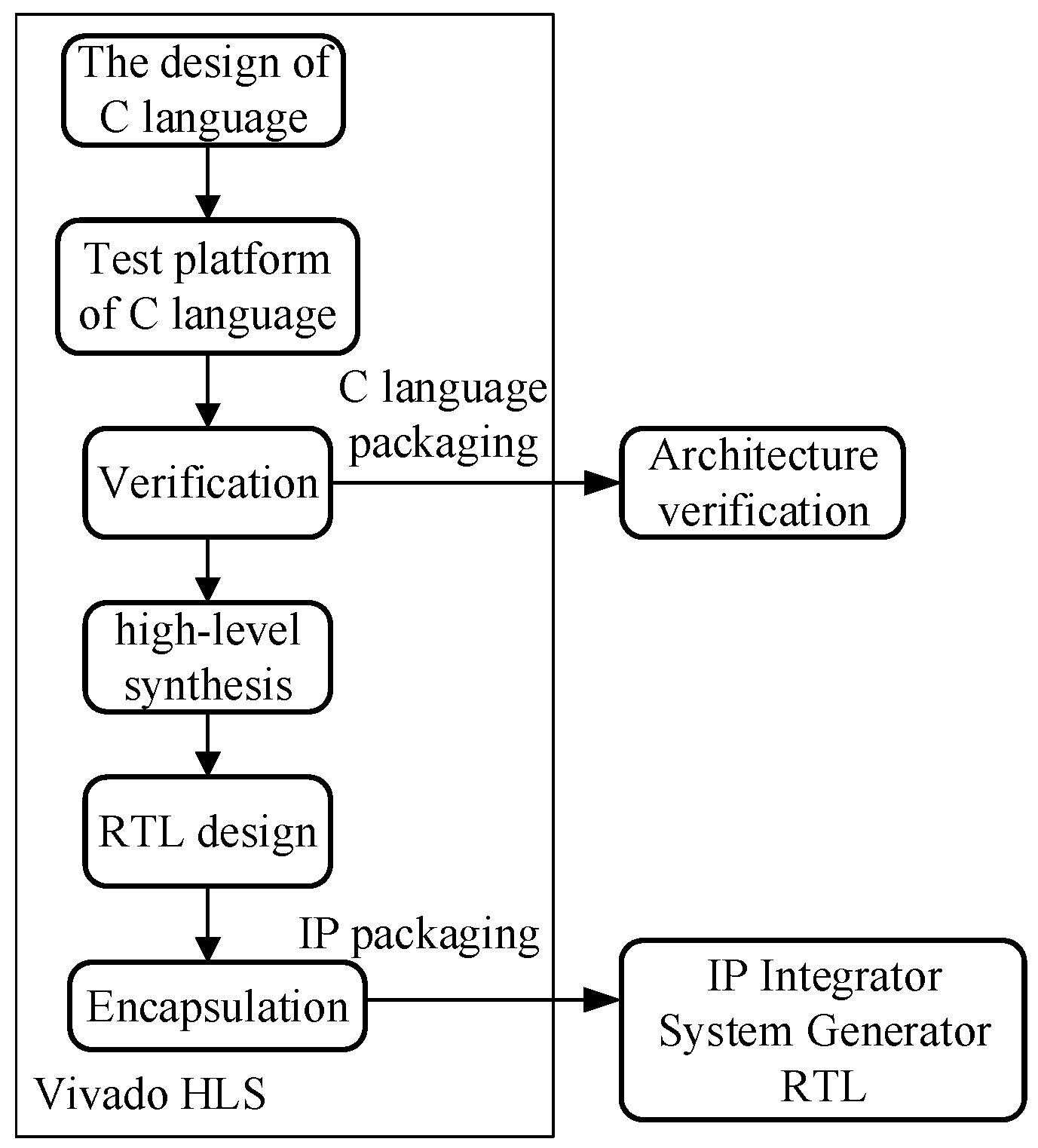
4.3. Vivado High-Level Synthesis
The programming of FPGAs is a complex task that requires developers to be proficient in the Hardware Description Language, while high-level synthesis tools allow programming in high-level languages such as C. This paper introduces the characteristics of high-level synthesis tools and uses it to finish simulation verification.
Vivado software is released by Xilinx in 2012 and is an upgraded version of ISE. It includes Vivado HLS tools, which can directly design FPGAs using C, C++, and System C. It is innovative, and it reduces the difficulty of FPGA-based design. It is an essential method for FPGA design in the future.
The development process of VHLS-based tools is shown in Figure 11. A specific function and test platform for the design is written by C or C++, and then the designed functionality is verified in the test platform. After meeting the functional requirements, the designed C model is converted into the corresponding Register Transfer Level ( RTL)design module by Vivado HLS tool, and then the established architecture and function are verified by a VHLS built-in simulator or encapsulated by an Internet Protocol (IP) encapsulator. Finally, modules are imported into the System Generator for functional verification at the RTL level.
5. Hardware in the Loop Simulation and Experiment
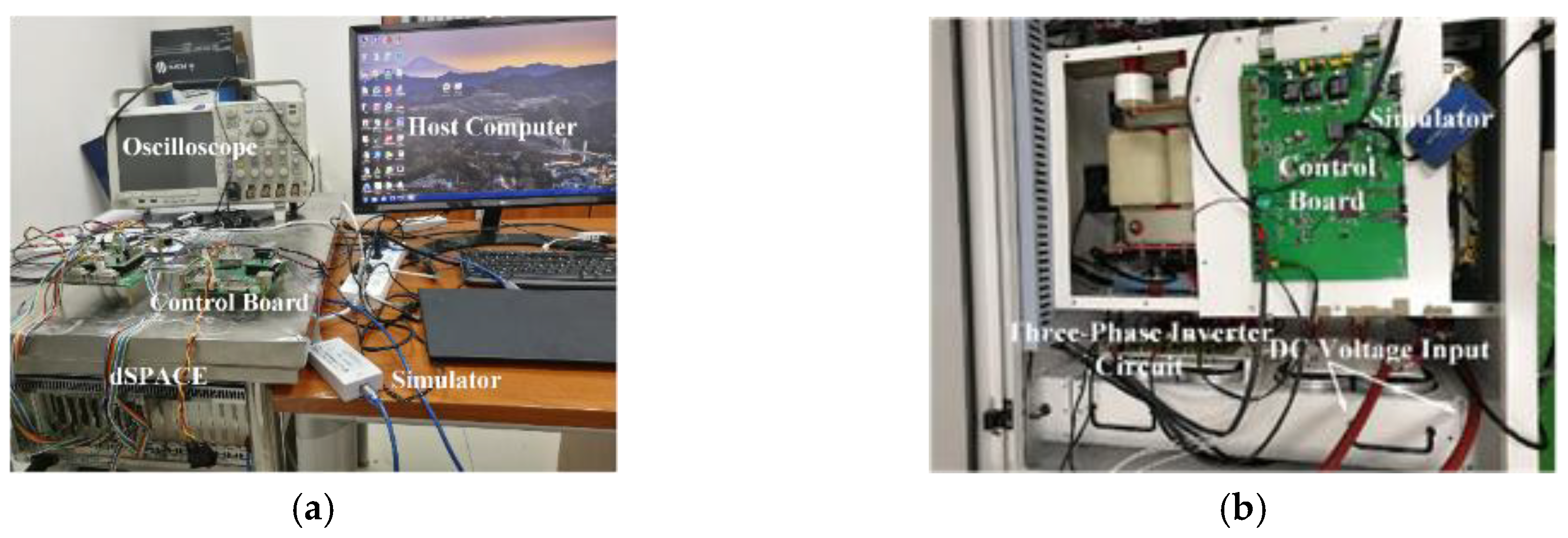
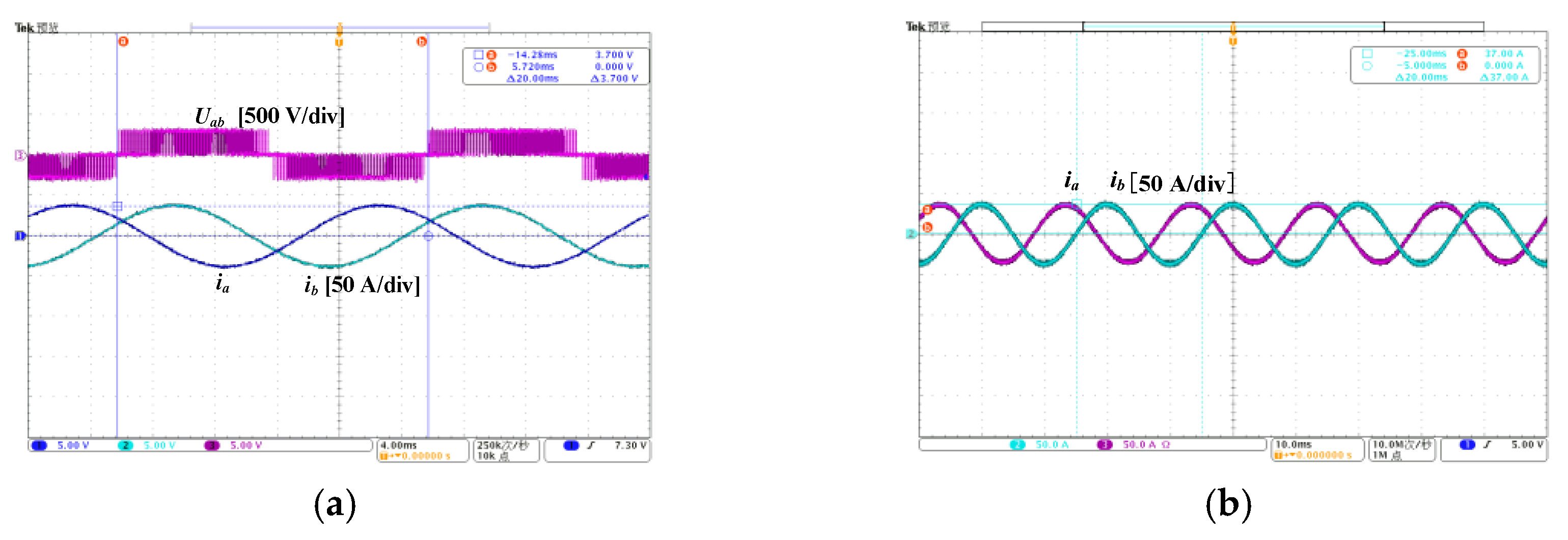
In order to demonstrate the validity of the ADC modeling optimization method, the test bench of HIL simulation and the practicality experiment platform, as shown in Figure 12, are constructed, respectively. The practicality experiment shares the same system parameters with the HIL simulation, which is listed in Table 1. The experimental results of the three-phase load currents obtained by the HIL simulation and the practicality experiment are shown in Figure 13.
In Figure 13a, the period of the switching voltage is 0.02 s and the amplitude is 300 V. Moreover, the amplitude of the simulation waveform of the three-phase load currents obtained by HIL simulation is 37 A. The relative error between it and the practicality experimental results is less than 0.7%, which verifies the validity of the ADC modeling optimization method.
The comparison of the FPGA resource usage of different bit-lengths in the HIL simulation is shown in Table 2. It can be seen that, as the bit-length decreases, the FPGA resources usage of Digital Signal Processing (DSPs), Slices, and LUTs (Look-Up-Table) are reduced. DSP mainly involves multiply-adder in digital circuits, and the reduction of bit-length has a significant influence on the decrease of DSP consumption (16.3%). A slice contains four LUTs, four flip-flops, and multiplexers, etc. LUTs are associated with combinatorial logic.
The reduction in bit-length has less effect on them, which are 1.78% and 1.58%, respectively. Therefore, it can be concluded that the proposed quantitative algorithm is valuable to minimize FPGA resources, especially for DSPs.
6. Discussion
Due to the fixed coefficient matrix, the ADC modeling method greatly reduces the number of computation times, which is achievable to conduct the real-time simulation of high switching frequency power converters. However, the equivalent substitution of the ADC discrete-time switch model introduces artificial oscillations. The minimum switching loss method proposed in this paper mitigates the oscillation error by selecting the optimal switch admittance parameters. Some scholars have also proposed some methods to select the appropriate Gs to improve the simulation results, but their methods are complicated and introduce other problems easily [3,18]. The minimum switching loss method is simple and effective, which improves the efficiency of modeling and the simulation.
In terms of FPGA resource optimization, this paper proposes a quantitative algorithm to choose the minimum bit-length and time step that meet the simulation accuracy to optimize FPGA resources. Due to the limited FPGA hardware resources, it is difficult to implement the FPGA-based real-time simulation of complex power electronic circuits. In the past literature, the empirical values of the bit-length and time step are always used in the FPGA implementation, which lacks systematic explanation. Some scholars have introduced the concept of SNR to calculate quantitatively the relationship between bit-length and digital signal accuracy [25,26,27]. Therefore, this paper further analyzes the SNR calculation, extends it to the modeling process of the power electronic converters, and studies the influence of time step on the simulation accuracy, which could calculate quantitatively the relationship among the bit-length, time step, and simulation accuracy. However, the SNR calculation theory still needs to be improved. For example, the influence of different coefficient bit-lengths on the model accuracy is not considered; therefore, more in-depth research will be conducted, but it is not within the scope of this paper.
7. Conclusions
This paper presents an ADC modeling optimization method by selecting an optimal switch admittance parameter, Gs, to improve the simulation precision. Compared with the existing methods, the proposed method reduces the amount of calculation and improves the simulation efficiency. It is worth noting that this method could be generalized to networks with an arbitrary number of switches. Moreover, a novel algorithm is presented to minimize the FPGA resources by calculating quantitatively the relationship of the time step, bit-length, and simulation precision. This paper is the first study to systematically analyze the impact of the bit-length and the time step on the model accuracy to choose the optimal bit-length and time step, which can help complex power electronic circuits achieve FPGA-based HIL real-time simulation. The proposed algorithm combined with the ADC modeling method is applied to the modeling and simulation process of the three-phase inverter. The Matlab/Power System Blockset is used as the offline benchmark platform for comparing the FPGA-based real-time simulation results and practicality experiment results. It is concluded that Gs = 0.0872 is the optimal parameter to reduce the oscillation and the bit-length ny = 25 and time step h=1e-7 s are the optimum value to optimize the FPGA resource and ensure the model accuracy at the same time. Therefore, FPGA-based real-time simulation and practicality experiments verify the validity of the ADC modeling method and the effect of FPGA resource optimization, respectively, which is of great significance for the research and development of discrete-time switch modeling and FPGA-implementation technology.
Author Contributions
Conceptualization, X.G.; data curation, J.Y.; formal analysis, J.Y. and Y.T.; funding acquisition, X.G. and X.Y.; investigation, J.Y. and Y.T.; methodology, J.Y.; project administration, X.G.; resources, X.G. and X.Y.; software, J.Y. and Y.T.; supervision, X.G. and X.Y.; validation, J.Y. and Y.T.; visualization, X.G. and J.Y.; writing—original draft preparation, J.Y.; writing—review and editing, X.G.
Funding
This research was funded by the National Natural Science Foundation of China, grant number 51777009.
Conflicts of Interest
The authors declare no conflict of interest.
References
- Zhang, B.; Hu, R.; Tu, S.; Zhang, J.; Jin, X.; Guan, Y.; Zhu, J. Modeling of Power System Simulation Based on FRTDS. Energies 2018, 11, 2749. [Google Scholar] [CrossRef]
- Leng, F.; Mao, C.; Wang, D.; An, R.; Zhang, Y.; Zhao, Y.; Cai, L.; Tian, J. Applications of Digital-Physical Hybrid Real-Time Simulation Platform in Power Systems. Energies 2018, 11, 2682. [Google Scholar] [CrossRef]
- Matar, M.; Iravani, R. FPGA Implementation of the Power Electronic Converter Model for Real-Time Simulation of Electromagnetic Transients. IEEE Trans. Power Deliv. 2010, 25, 852–860. [Google Scholar] [CrossRef]
- Zhang, B.; Wang, Y.; Tu, S.; Jin, Z. FPGA-Based Real-Time Digital Solver for Electro-Mechanical Transient Simulation. Energies 2018, 11, 2650. [Google Scholar] [CrossRef]
- Li, J.; Li, X.; Du, L.; Cao, M.; Qian, G. An Intelligent Sensor for the Ultra-High-Frequency Partial Discharge Online Monitoring of Power Transformers. Energies 2016, 9, 383. [Google Scholar] [CrossRef]
- Zhang, B.; Wu, Y.; Jin, Z.; Wang, Y. A Real-Time Digital Solver for Smart Substation Based on Orders. Energies 2017, 10, 1795. [Google Scholar] [CrossRef]
- Zhang, B.; Nie, S.; Jin, Z. Electromagnetic Transient-Transient Stability Analysis Hybrid Real-Time Simulation Method of Variable Area of Interest. Energies 2018, 11, 2620. [Google Scholar] [CrossRef]
- Stifter, M.; Cordova, J.; Kazmi, J.; Arghandeh, R. Real-Time Simulation and Hardware-in-the-Loop Testbed for Distribution Synchrophasor Applications. Energies 2018, 11, 876. [Google Scholar] [CrossRef]
- Benhalima, S.; Miloud, R.; Chandra, A. Real-Time Implementation of Robust Control Strategies Based on Sliding Mode Control for Standalone Microgrids Supplying Non-Linear Loads. Energies 2018, 11, 2590. [Google Scholar] [CrossRef]
- Garcia, J.; Garcia, P.; Capponi, F.G.; Donato, G.D. Analysis, Modeling, and Control of Half-Bridge Current-Source Converter for Energy Management of Supercapacitor Modules in Traction Applications. Energies 2018, 11, 2239. [Google Scholar] [CrossRef]
- Priyadarshi, N.; Padmanaban, S.; Lonel, D.M.; Mihet-Popa, L.; Azam, F. Hybrid PV-Wind, Micro-Grid Development Using Quasi-Z-Source Inverter Modeling and Control—Experimental Investigation. Energies 2018, 11, 2277. [Google Scholar]
- Sudha, S.A.; Chandrasekaran, A.; Rajagopalan, V. New approach to switch modelling in the analysis of power electronic systems. IEE Proc. B Electr. Power Appl. 1993, 140, 115–123. [Google Scholar] [CrossRef]
- Wedepohl, L.M.; Jackson, L. Modified nodal analysis: An essential addition to electrical circuit theory and analysis. Eng. Sci. Educ. J. 2002, 11, 84–92. [Google Scholar] [CrossRef]
- Blij, N.H.V.D.; Ramirez-Elizondo, L.M.; Spaan, M.; Bauer, P. A State-Space Approach to Modelling DC Distribution Systems. IEEE Trans. Power Syst. 2018, 33, 943–950. [Google Scholar] [CrossRef] [Green Version]
- Kiffe, A.; Geng, S.; Schulte, T. Automated generation of a FPGA-based oversampling model of power electronic circuits. In Proceedings of the 15th International Power Electronics and Motion Control Conference (EPE/PEMC), Novi Sad, Serbia, 4–6 September 2012. [Google Scholar]
- Hui, S.Y.R.; Christopoulos, C. A discrete approach to the modeling of power electronic switching networks. IEEE Trans. Power Electron. 1990, 5, 398–403. [Google Scholar] [CrossRef]
- Dufour, C.; Cense, S.; Ould-Bachir, T.; Gregoire, L. General-purpose reconfigurable low-latency electric circuit and motor drive solver on FPGA. In Proceedings of the 38th Annual Conference on IEEE Industrial Electronics Society (IECON), Montréal, QC, Canada, 25–28 October 2012; pp. 3073–3081. [Google Scholar]
- Maguire, T.; Giesbrecht, J. Small time-step (< 2usec) VSC model for the real time digital simulator. In Proceedings of the International Conference on Power Systems Transients (IPST’05), Montreal, QC, Canada, 20–23 June 2005. [Google Scholar]
- Matar, M.; Iravani, R. An FPGA-based real-time digital simulator for power electronic systems. In Proceedings of the International Conference on Power Systems Transients (IPST’07), Lyon, France, 4–7 June 2007. [Google Scholar]
- Miceli, R.; Schettino, G.; Viola, F. A Novel Computational Approach for Harmonic Mitigation in PV Systems with Single-Phase Five-Level CHBMI. Energies 2018, 11, 2100. [Google Scholar] [CrossRef]
- Nicolas-Apruzzese, J.; Lupon, E.; Busquets-Monge, S.; Conesa, A.; Bordonau, J.; García-Rojas, G. FPGA-Based Controller for a Permanent-Magnet Synchronous Motor Drive Based on a Four-Level Active-Clamped DC-AC Converter. Energies 2018, 11, 2639. [Google Scholar] [CrossRef]
- Baptista, D.; Mostafa, S.S.; Pereira, L.; Sousa, L.; Morgado-Dias, F. Implementation Strategy of Convolution Neural Networks on Field Programmable Gate Arrays for Appliance Classification Using the Voltage and Current (V-I) Trajectory. Energies 2018, 11, 2460. [Google Scholar] [CrossRef]
- Ricco, M.; Mathe, L.; Monmasson, E.; Teodorescu, R. FPGA-Based Implementation of MMC Control Based on Sorting Networks. Energies 2018, 11, 2394. [Google Scholar] [CrossRef]
- Nguyen-Van, T.; Abe, R.; Tanaka, K. Digital Adaptive Hysteresis Current Control for Multi-Functional Inverters. Energies 2018, 11, 2422. [Google Scholar] [CrossRef]
- Schlecker, W.; Beuschel, C.; Pfleiderer, H.J. Analytical consideration of the quantization error in basic arithmetic operations of digital signal processing. Adv. Radio Sci. 2005, 3, 343–347. [Google Scholar] [CrossRef]
- Schlecker, W. Quantization Effects in Digital Signal Processing; The University of Ulm: Ulm, Germany, 2006. [Google Scholar]
- Li, Y.; Zhu, T.; Cao, Z. Analysis of Influence of Time Step on Numerical Simulation of Finite Volume Method. Comput. Simul. 2009, 26, 117–120. [Google Scholar]
- Kim, Y.M.; Shin, D.G.; Kim, C.G. Optimization of Design Pressure Ratio of Positive Displacement Expander for Vehicle Engine Waste Heat Recovery. Energies 2014, 7, 6105–6117. [Google Scholar] [CrossRef] [Green Version]
- Dang, H.S.; Wang, L.; Wang, X.Q. Development and application of FPGA based on Vivado HLS. J. Shaanxi Univ. Sci. Technol. 2015, 33, 341–361. [Google Scholar]
- Lei, J.; Li, Y.; Zhao, D.; Xie, J.; Chang, C.; Wu, L.; Li, X.; Zhang, J.; Li, W. A Deep Pipelined Implementation of Hyperspectral Target Detection Algorithm on FPGA Using HLS. Remote Sens. 2018, 10, 516. [Google Scholar] [CrossRef]
- Huang, H.; Zhai, L.; Wang, Z. A Power Coupling System for Electric Tracked Vehicles during High-Speed Steering with Optimization-Based Torque Distribution Control. Energies 2018, 11, 1538. [Google Scholar] [CrossRef]
- Guillo-Sansano, E.; Syed, M.H.; Roscoe, A.J.; Burt, G.M. Initialization and Synchronization of Power Hardware-In-The-Loop Simulations: A Great Britain Network Case Study. Energies 2018, 11, 1087. [Google Scholar] [CrossRef]
- Rodič, M.; Milanovič, M.; Truntič, M. Digital Control of an Interleaving Operated Buck-Boost Synchronous Converter Used in a Low-Cost Testing System for an Automotive Powertrain. Energies 2018, 11, 2290. [Google Scholar] [CrossRef]
Figure 1.
Associated Discrete Circuit (ADC) switch model: (a) on; (b) off.

Figure 2.
Three-phase inverter with LC filter.

Figure 3.
The commutation process of sw1 (i1 > 0): (a) From OFF to ON; (b) From ON to OFF.

Figure 4.
Equivalent circuit of the three-phase inverter.

Figure 5.
Switching loss trend with the switch admittance parameter (Gs).

Figure 6.
Switching voltage: (a) h = 5e-7 s; (b) h = 1e-7 s; (c) h = 1e-8 s.

Figure 7.
Three-phase current comparison: (a) three-phase current of inverter side; (b) relative error; (c) three-phase current of load side; (d) relative error.
Figure 7.
Three-phase current comparison: (a) three-phase current of inverter side; (b) relative error; (c) three-phase current of load side; (d) relative error.

Figure 8.
Probability density function.

Figure 9.
Signal-to-noise (SNR) Surface Plot.

Figure 10.
Error Comparison Diagram.

Figure 11.
Vivado High-Level Synthesis (VHLS) development process.

Figure 12.
Experimental test bench: (a) hardware in the loop (HIL) simulation; (b) Practicality experiment.
Figure 12.
Experimental test bench: (a) hardware in the loop (HIL) simulation; (b) Practicality experiment.

Figure 13.
Three-phase load current waveform: (a) HIL simulation; (b) practicality experiment.


Table 1.
System parameter.
| Parameters | Unit | Value |
|---|---|---|
| DC voltage | V | 300 |
| Switching frequency | kHz | 10 |
| Fundamental modulation frequency | Hz | 50 |
| Inductance L | H | 1.2 × |
| Capacitance C | F | 2 × |
| Load resistance R | Ω | 4 |
| Admittance parameter Gs | mH | 0.0872 |
| Duty circle | - | 0.9 |
Table 2.
Field-programmable gate (FPGA) resource usage comparison with different bit-lengths.
| FPGA Resource | 25 | 28 | 31 | Available |
|---|---|---|---|---|
| Slice | 4910 | 5560 | 5821 | 50,950 |
| LUTs | 13,439 | 16,207 | 16,653 | 203,800 |
| DSPs | 337 | 468 | 474 | 840 |
© 2018 by the authors. Licensee MDPI, Basel, Switzerland. This article is an open access article distributed under the terms and conditions of the Creative Commons Attribution (CC BY) license (http://creativecommons.org/licenses/by/4.0/).
Share and Cite
MDPI and ACS Style
Guo, X.; Yuan, J.; Tang, Y.; You, X. Hardware in the Loop Real-time Simulation for the Associated Discrete Circuit Modeling Optimization Method of Power Converters. Energies 2018, 11, 3237. https://doi.org/10.3390/en11113237
AMA Style
Guo X, Yuan J, Tang Y, You X. Hardware in the Loop Real-time Simulation for the Associated Discrete Circuit Modeling Optimization Method of Power Converters. Energies. 2018; 11(11):3237. https://doi.org/10.3390/en11113237
Chicago/Turabian StyleGuo, Xizheng, Jiaqi Yuan, Yiguo Tang, and Xiaojie You. 2018. "Hardware in the Loop Real-time Simulation for the Associated Discrete Circuit Modeling Optimization Method of Power Converters" Energies 11, no. 11: 3237. https://doi.org/10.3390/en11113237
Note that from the first issue of 2016, this journal uses article numbers instead of page numbers. See further details here.