1. Introduction
Since power systems with a DC distribution method has many advantages, such as conversion efficiency increase of about 5–10%, cost reducing by about 15–20% and so on, the AC distribution power system will be replaced by a DC distribution one [
1].
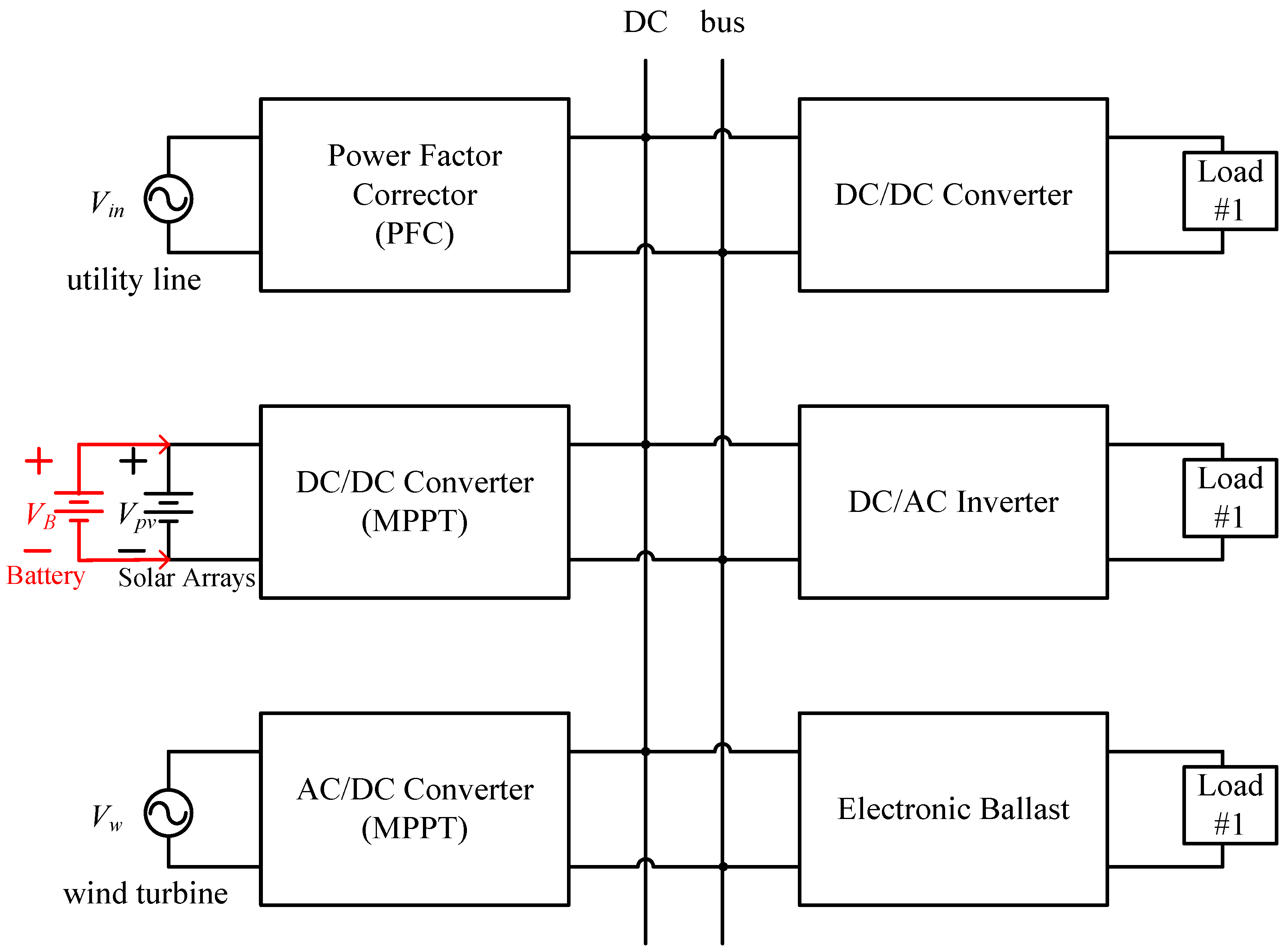
Figure 1 shows a block diagram of a power system for DC load applications. The power sources of the power system can adopt utility line, solar arrays, battery or wind turbine, etc. The power system using a power processor is widely applied to the general electrical or electronic equipment. In order to obtain a lighter weight and a smaller volume, a switching-mode converter is regarded as the power processor of the power system. When a power factor corrector (PFC) is used for the AC/DC power system [
2,
3,
4,
5,
6,
7,
8,
9,
10,
11,
12] to protect the line source from harmonic current pollution, it has to meet the recommended limits of harmonics in supply current by various international power quality standards, such as the International Electrotechnical Commission (IEC) 61000-3-2 [
2]. Therefore, the AC/DC converter adopts PFC techniques to increase power factor (PF), in which input voltage waveform can be made to be completely in phase with the input current one, implying approximately unity power factor.
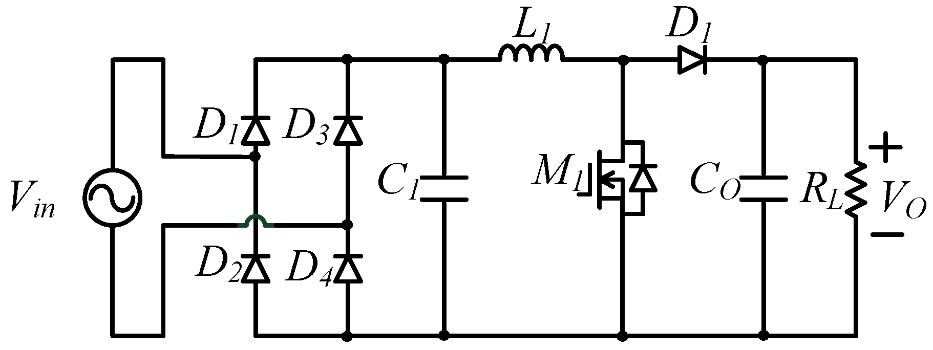
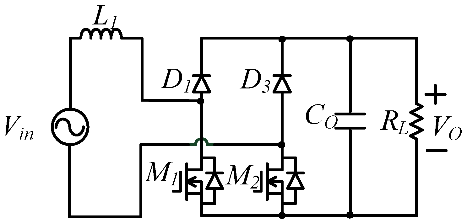
In general, a boost converter, as shown in
Figure 2, or buck-boost converter is adopted in the PFC system. In order to reduce the conduction losses of diodes, a bridgeless boost converter is adopted to achieve a higher power factor, as shown in
Figure 3. Due to the universal input voltage source (AC 90–265 V), its output voltage is regulated at approximately 400 V. For a power system under a lower level output voltage condition, it needs an extra DC/DC converter as a step-down converter. Therefore, the topology of two stages is used to achieve a lower output voltage, resulting in a higher cost and a lower conversion efficiency. Single stage topology with buck-boost converter has been an alternative solution in various power conversions. In order to further increase the step-down ratio, a bridgeless flyback converter is regarded as the power processor because of its topological advantages, such as simple circuit structure, low cost, and galvanic isolation, as depicted in
Figure 4. It is adopted in not only low power isolated single-stage single-phase AC/DC converters which is regarded as the front end of the switching-mode power supply, but also uninterrupted power supplies (UPS), induction heating, electronic ballast, telecom power supplies, light emitting diode drivers [
13,
14,
15], etc.
Since a flyback converter adopts a transformer to be regarded as a stored inductor and an isolated transformer, a leakage inductance exists in the primary side, resulting in a higher voltage stress across switches of the converter when switches are turned off. In order to limit a high voltage stress across switches, a resistor-capacitor-diode (RCD) clamp circuit is used to reduce switch voltage spike. Although the RCD circuit can smooth out the voltage spike, the energy stored in leakage inductance is released to the clamp resistor. As a result, the conversion efficiency of the flyback converter does not increase. For improving conversion efficiency of the one with the RCD clamp circuit, an active clamp circuit is used to replace the RCD clamp circuit, as shown in
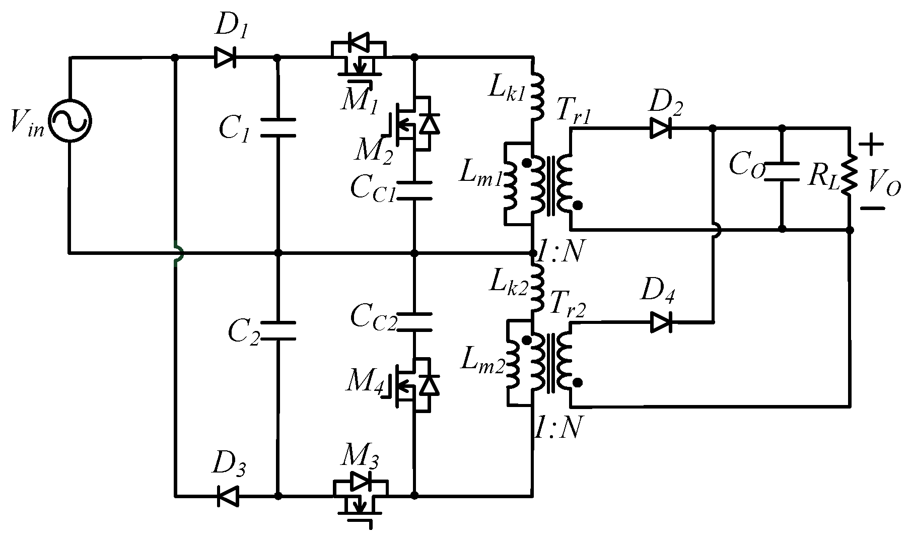
Figure 5. With this approach, the energy stored in leakage inductance can be recycled and switches in the converter can be operated with zero-voltage switching (ZVS) at the turn-on transition [
16,
17].
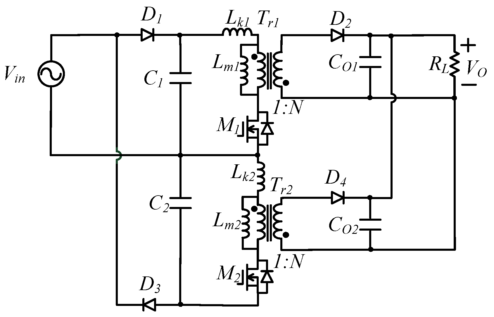
When the PFC adopts a bridgeless flyback converter, it needs to process power in a positive and negative half periods of the line source, resulting in that its component counts almost need twofold of its counterpart circuit [
18,
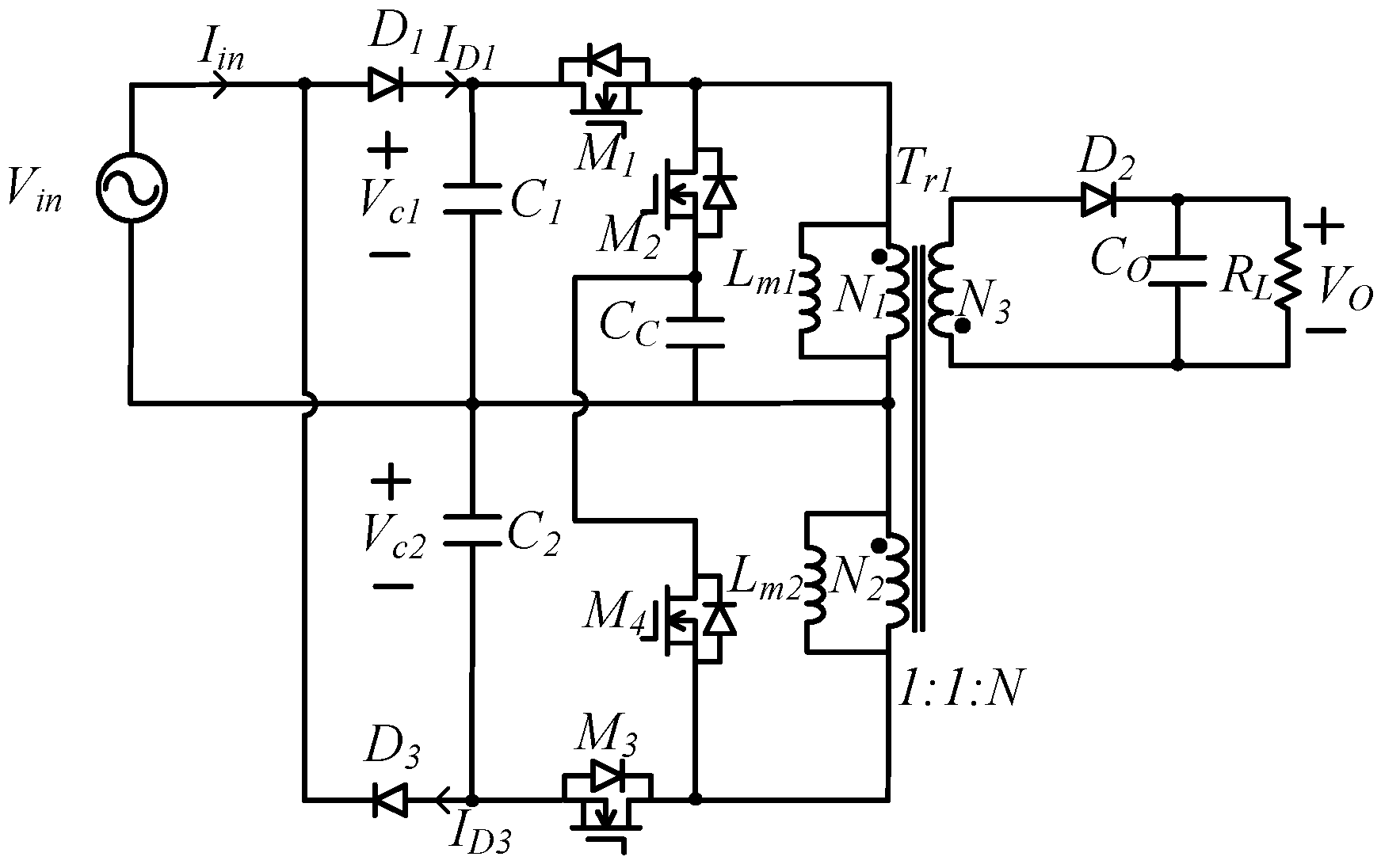
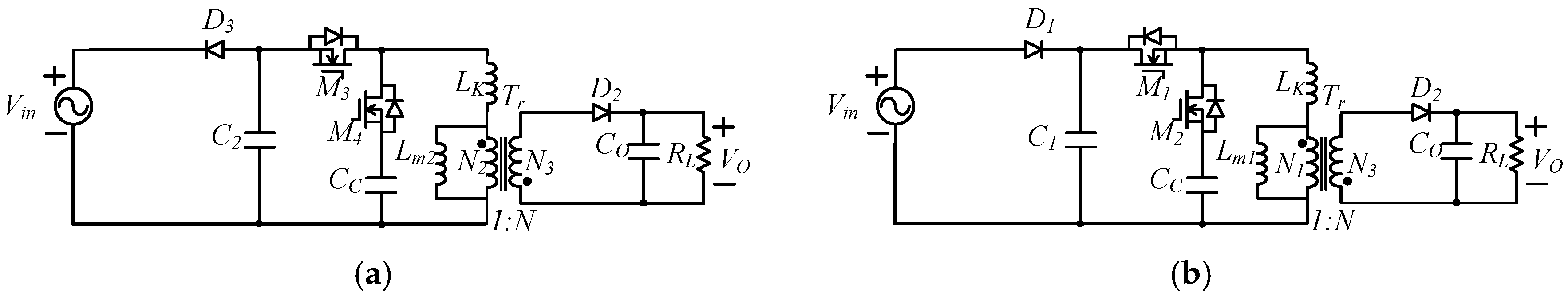
19]. Particularly, using more than one magnetic device in the bridgeless flyback converter impacts the advantage, which is the circuit simplicity. In order to further simplify the circuit structure, two transformers in the bridgeless flyback converter is replaced with a three-winding transformer, as illustrated in
Figure 6. Furthermore, two active clamp circuits share a capacitor. It will reduce weight, volume and component counts, significantly.
This paper proposes a bridgeless flyback converter, illustrating that the proposed one is without bridge diodes to remove the diode conduction loss and increase conversion efficiency. In addition, the proposed one adopts a three-winding transformer to substitute for two transformers. When the output maximum power of the proposed bridgeless flyback is the same as that of the conventional bridgeless flyback converter, as shown in
Figure 5, its maximum input current
Ii is also the same as each other, and maximum working flux
Bpk of the transformer in the proposed converter is also the same as that in the conventional bridgeless flyback converter.
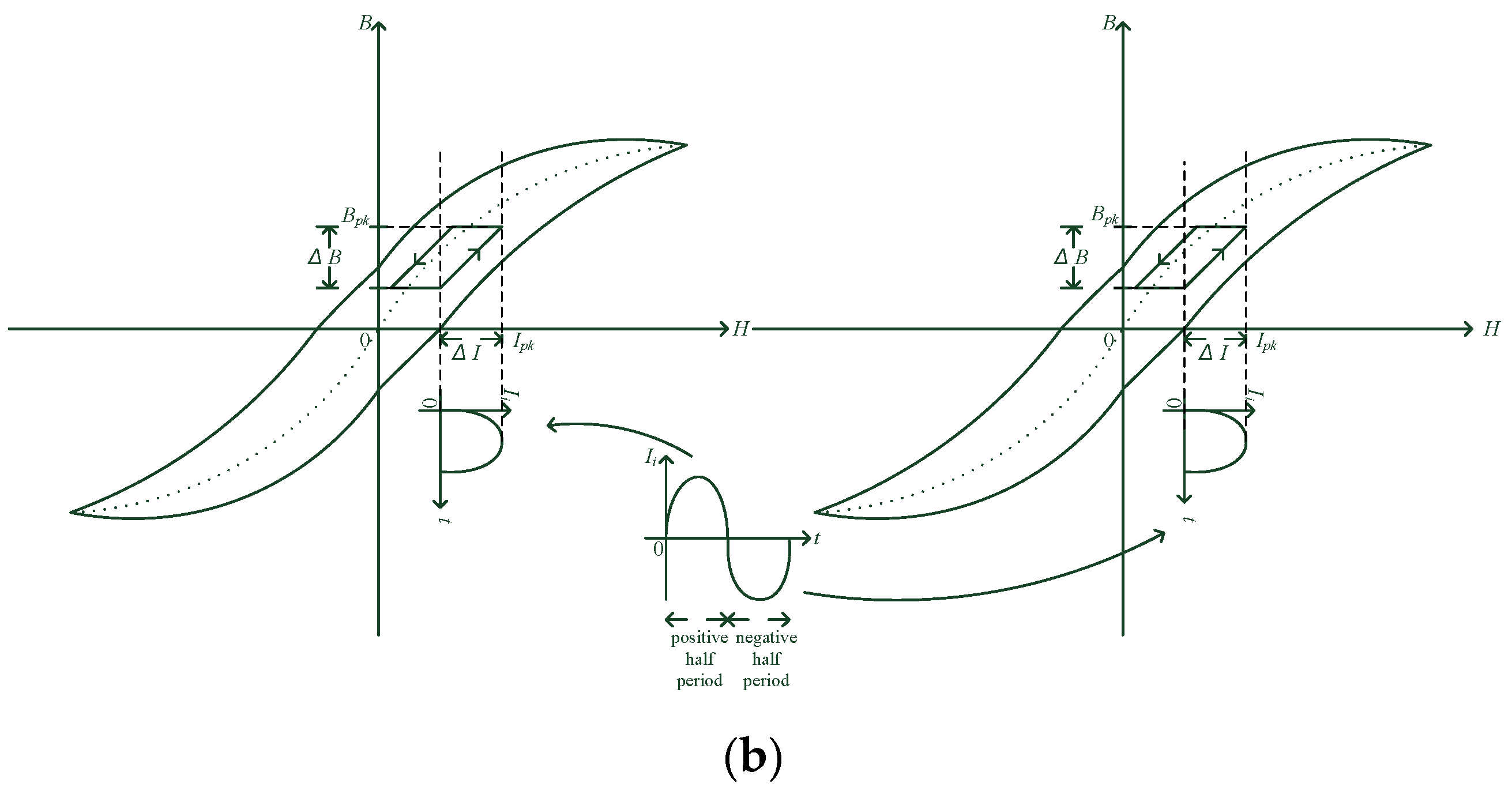
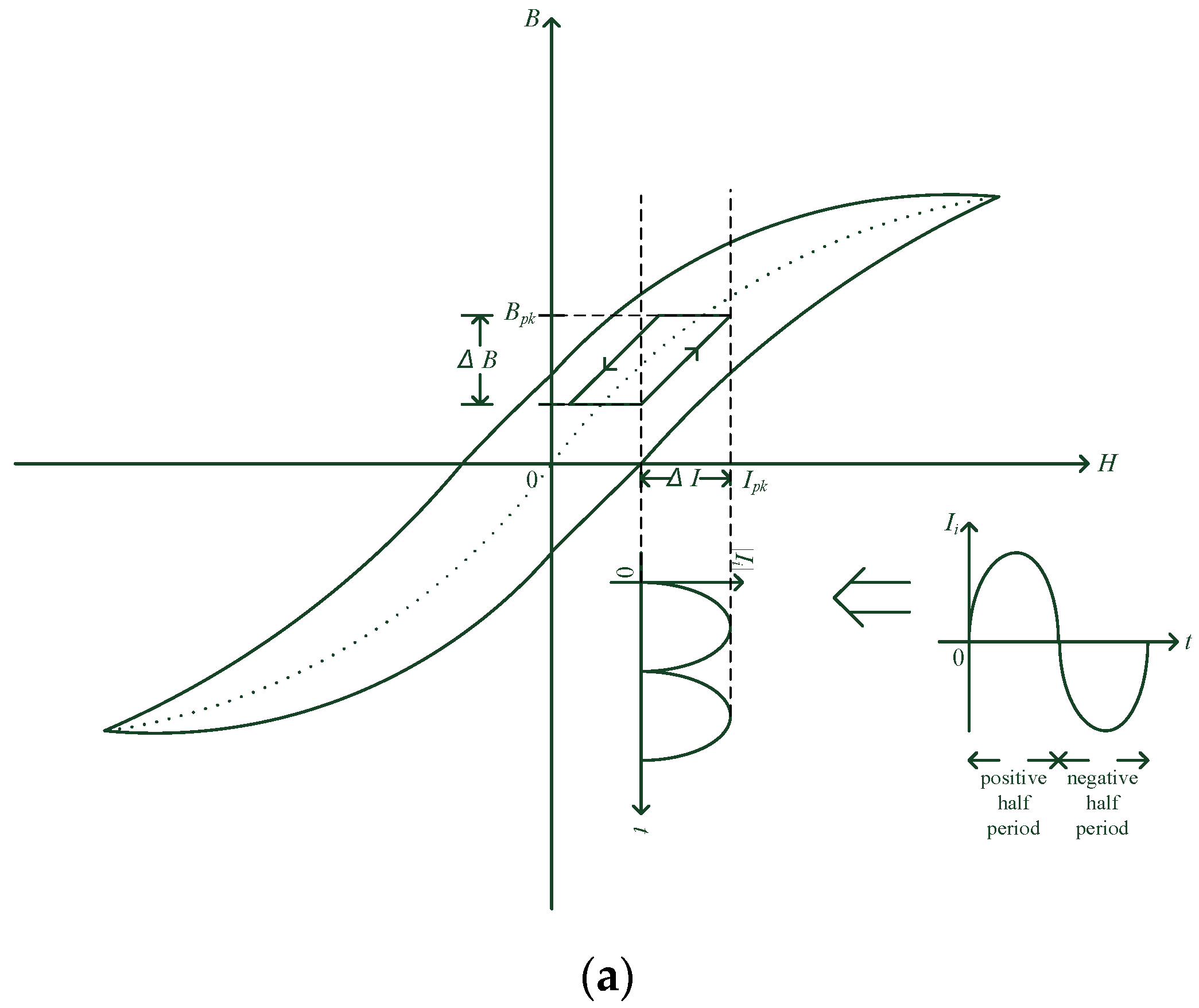
Figure 7 shows a B-H curve of the transformer
Tr in the flyback converter. Since the conventional flyback converter uses a bridge rectifier to rectify input current
Ii, the rectified input current
Ii can be obtained by a positive value during a complete switching cycle. Its B-H curve is illustrated in
Figure 7a. As a result, the conventional flyback converter can use a set of transformers to implement PFC function. While, the bridgeless flyback converter, as shown in
Figure 5, needs two sets of transformers to process energy under the positive half period and the negative half period. Its B-H curve is illustrated in
Figure 7b. Due to the proposed bridgeless flyback converter with a three-winding transformer, its B-H curve is the same as the conventional flyback one, as shown in
Figure 7a. Therefore, the proposed bridgeless converter can save a set of transformers. It can simplify the circuit structure, significantly. Therefore, the proposed bridgeless flyback converter for the PFC power system can achieve a higher power factor to avoid the line source from harmonic pollution, possesses soft-switching features in which switches are operated in ZVS at turn-on transition to increase conversion efficiency. It is suitable for a low power level application. This paper focuses on design and analysis of the proposed bridgeless flyback converter and power management for DC loads of power system.
2. Control Algorithm of the Proposed System for DC Load Applications
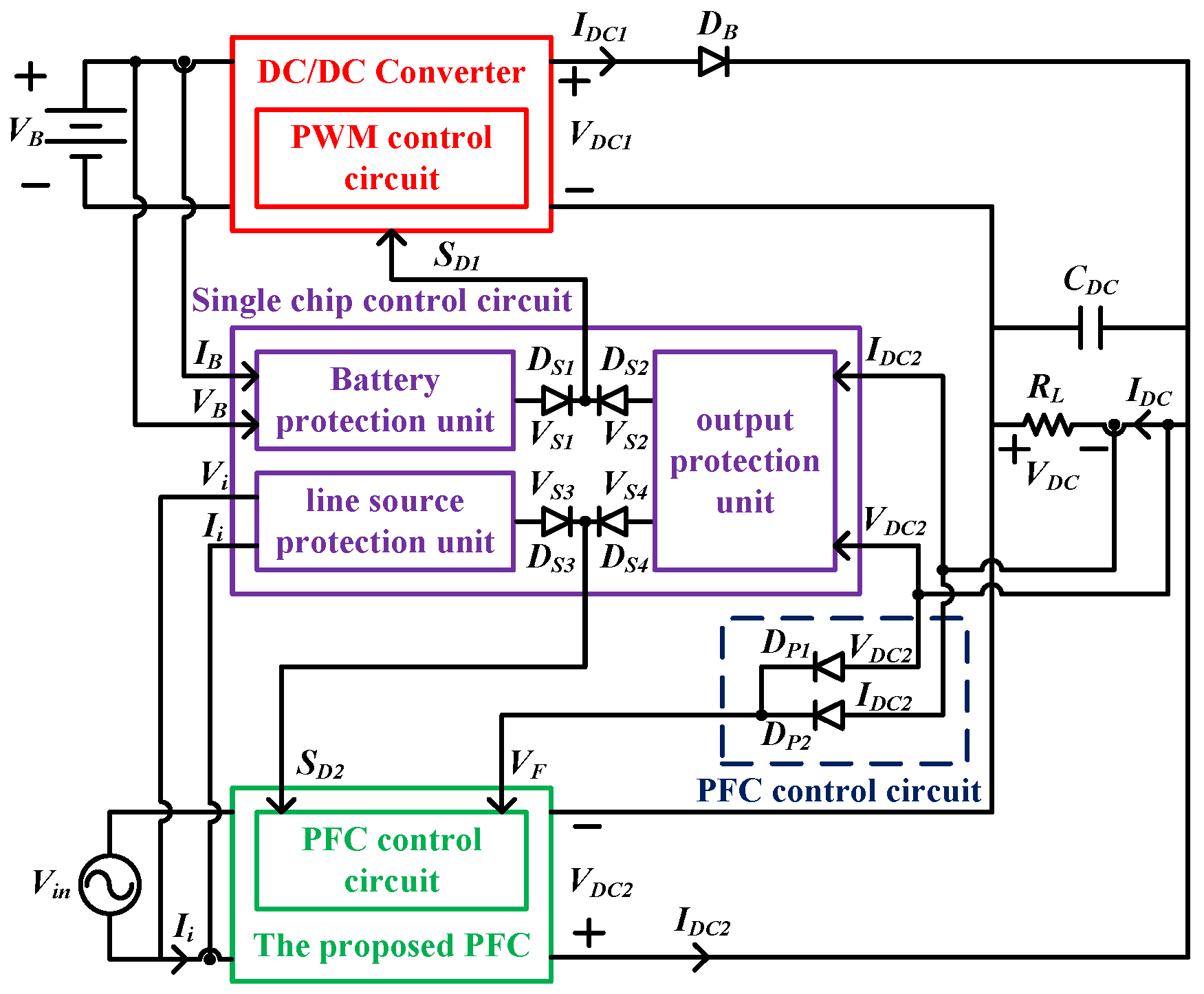
The proposed bridgeless PFC is applied to a DC load power system. In order to implement a DC load power system, the proposed one and a DC/DC converter with a battery source connected in parallel to supply power for DC loads. Its block diagram is shown in
Figure 8. The control algorithm of the proposed power system for DC load applications is described in the following sections.
1. Circuit Topology of the Proposed Power System
The proposed DC load power system consists of a DC/DC converter with a battery source and a bridgeless PFC and single-chip control circuit. The output voltage VDC2 of the bridgeless PFC is close to and is greater than the output voltage VDC1 of the DC/DC converter. Therefore, the diode DB is used to block the voltage difference between voltages VDC2 and VDC1. The DC load RL is supplied power from the proposed PFC and the DC/DC converter. When the load power PL is less than or equal to PDC2(max) which is the maximum output power of the proposed PFC, the proposed PFC supplies power to load. If PL is greater than PDC2(max), the proposed PFC and the DC/DC converter supply power to load for achieving a DC load power system.
2. Control Algorithm of Each Unit
● DC/DC converter
The DC/DC converter adopts a boost converter with a single-capacitor snubber [
20]. It can transfer power from the battery to load. Since its output voltage
VDC1 is less than the voltage
VDC2, a diode
DB is used to protect the DC/DC converter. Therefore, the protection diode with the output diode of boost converter is replaced by the extra diode
DB. If the operational state is in the 0 <
PL ≤
PDC2(max) state, the battery with the DC/DC converter can be operated in the charging mode. It needs an extra charger to charge the battery. When the proposed power system is operated in an abnormal state, the single-chip control circuit sends a shutdown signal
SD1 under a high level to the pulse width modulation (PWM) control circuit of the DC/DC converter. The DC/DC converter can be operated in the shutdown state to protect the DC/DC one.
● The Proposed PFC
The proposed PFC uses a bridgeless flyback converter which is regarded as a power factor corrector for increasing power factor between input voltage and input current of a line source. Its control circuit adopts a PWM IC for PFC control.
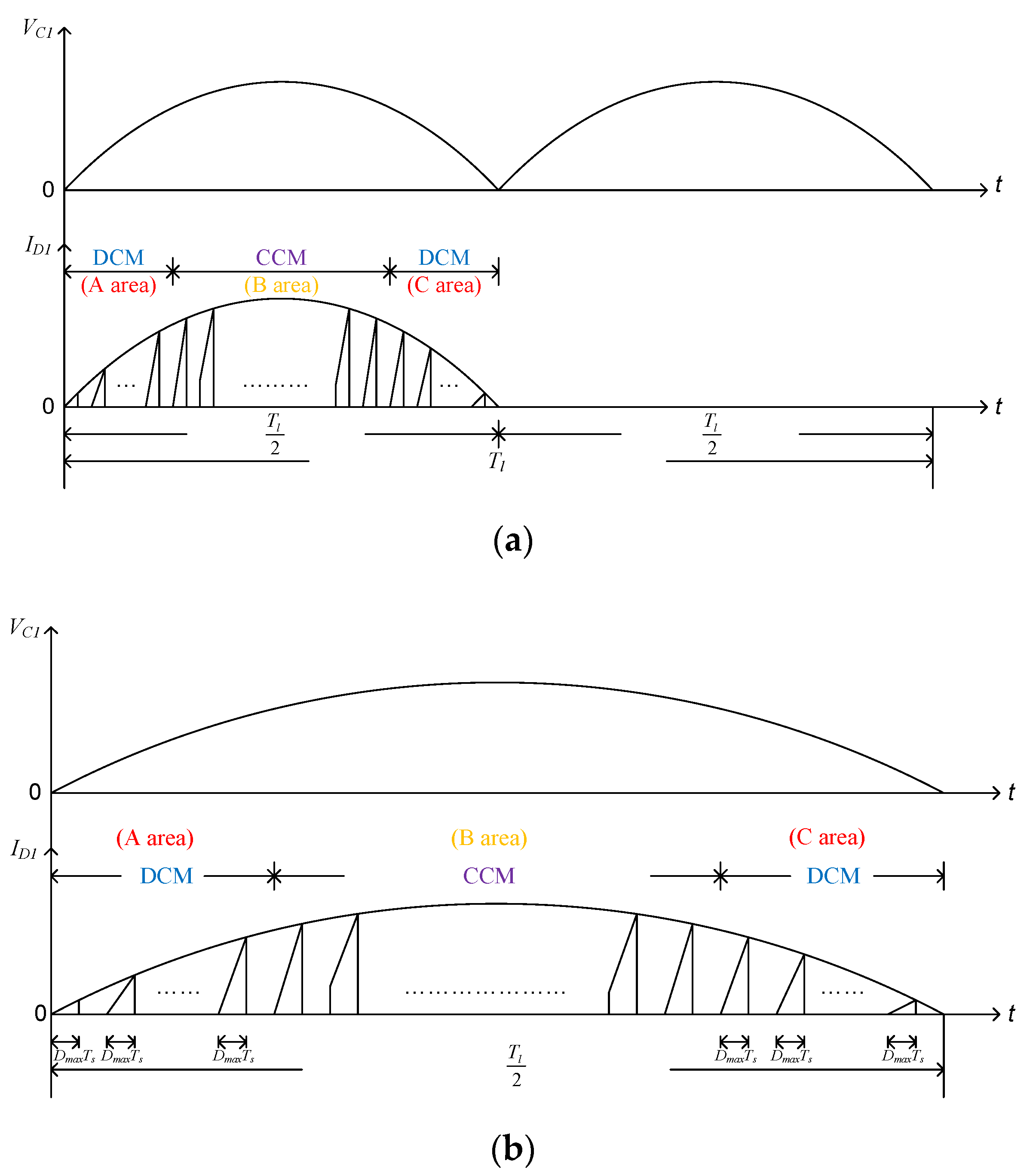
Figure 9 illustrates conceptual waveforms of voltage
VC1 and current
ID1. Variation of current
ID1 follows the sine waveform of input voltage
VC1.
Figure 9a shows concept waveforms under a complete line period, while
Figure 9b depicts those waveforms under a positive half period. From
Figure 9b, it can be seen that the proposed flyback converter can be operated in discontinuous conduction mode (DCM) or continuous conduction mode (CCM) under a positive half period. When the proposed one is operated in the A and C areas, inductor current
ILK is in the DCM state due to a lower voltage level of input voltage
VC1. If input voltage
VC1 is during the B area interval, the proposed converter is operated in CCM. According to the operational method of the proposed one as mentioned above, input voltage
Vin and current
Ii are in phase. Therefore, the proposed flyback converter can increase PF and reduce total harmonic distortion (THD).
In
Figure 8, when output current
IDC2 of the proposed PFC is less than or is equal to the maximum output current
IDC2(max), the output feedback voltage
VF is equal
VDC2 (diode
DP1 is forward biased). The proposed PFC is operated as the voltage regulator. If
IDC2 is greater than
IDC2(max), the output current
IDC2 is regulated at
IDC2(max). That is, the proposed one is operated as the current regulator. The voltage
VF is equal to
IDC2(max) and the diode
DP2 is in the forwardly bias state. In addition, when the proposed power system has an abnormal operational condition, the shutdown signal voltage
SD2 is changed from a low level to a high level. The proposed PFC is shut down to protect the proposed one.
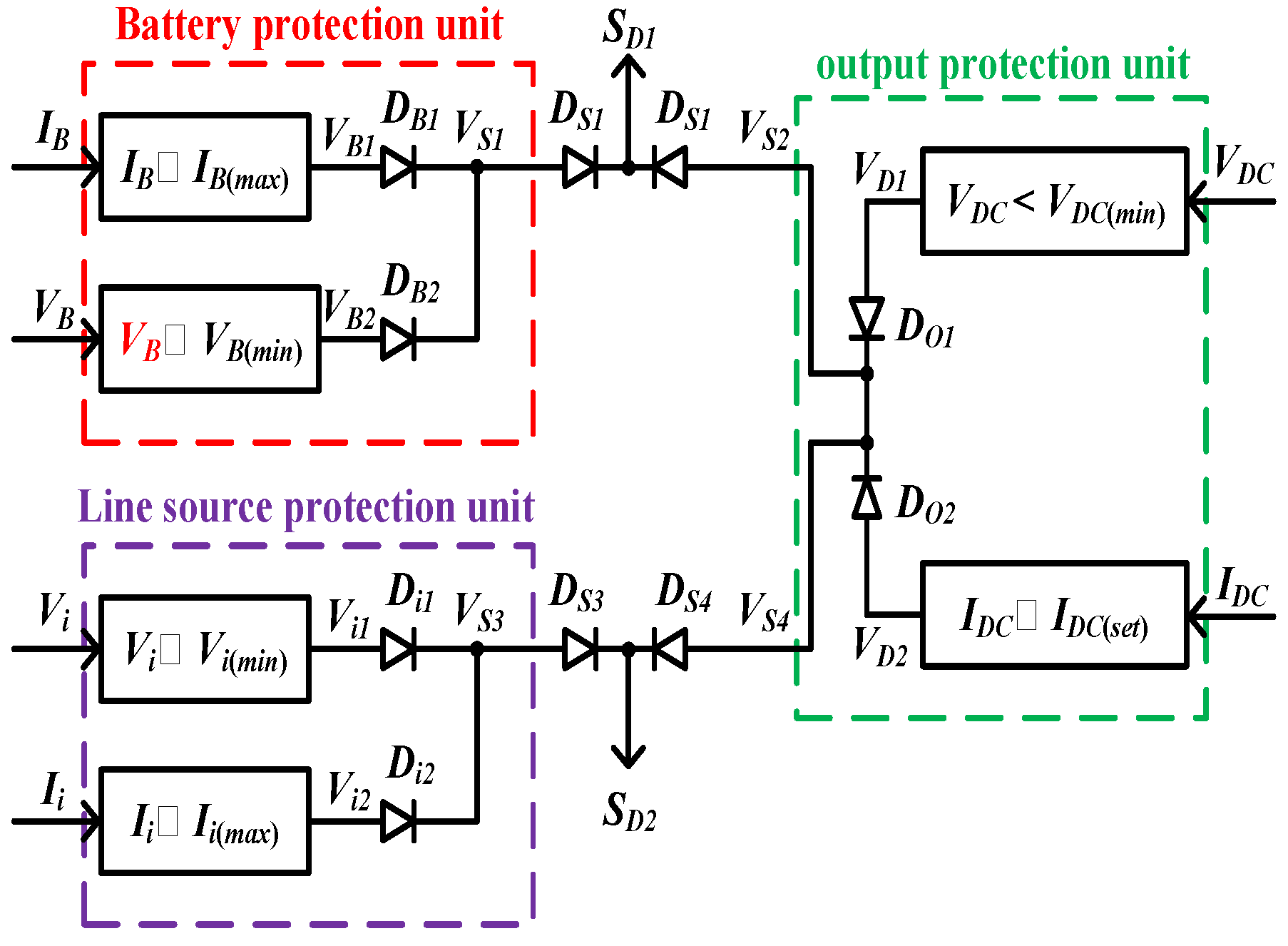
3. Single-Chip Control Circuit
The single-chip control circuit includes three units: The battery protection unit, line source protection unit and output protection unit. According to the operational relationships between DC/DC converter and the proposed PFC, the operational cases are divided into four cases, as listed in
Table 1. Symbol definition of the proposed power system is listed in
Table 2. Their operational conditions are described in the following section.
● Case I: PL = 0 W
When PL = 0 W, the DC/DC converter with battery source and the proposed PFC are operated in the shutdown mode.
● Case II: 0 < PL ≤ PDC2(max)
When 0 < PL ≤ PDC2(max), PB = 0 W and PDC2 = PL. The DC/DC converter with battery source and the proposed PFC with line source are operated in the working state.
● Case III: PDC2(max) < PL ≤ PDC2(max) + PB(max)
When PDC2(max) < PL ≤ PDC2(max) + PB(max), PDC2 = PDC2(max) and PB = PL − PDC2(max). The DC/DC converter and the proposed PFC are in the working state.
● Case IV: PL > PDC2(max) + PB(max)
When PL > PDC2(max) + PB(max), the proposed power system is operated in the over-load state. Therefore, the DC/DC converter and the proposed PFC are in the shutdown state.
There are three protection units in the proposed power system: Battery protection, line source protection and output protection units. In order to increase protections of the proposed power system, hardware and software methods are adopted to protect the proposed one. Due to the same protection functions between hardware and software methods, the operation of hardware protection circuit is introduced in this paper.
Figure 10 shows a block diagram of the single chip control circuit for the hardware protection circuit. In the battery protection unit, when
IB >
IB(max), the discharging current
IB is in the over-current state. Voltage
VB1 is changed from a low level to a high level. Voltage
SD1 is equal to
VS1 (=
VB1). The DC/DC converter is shut down to protect the battery. If
VB <
VB(min), the battery is in the under-voltage state. Voltage single
VB2 is changed from a low level to a high level, and signal
SD1 is the same as
VS1 (=
VB2). Therefore, the DC/DC converter is also shut down.
In the line source protection unit, when Vi < Vi(min) (=AC 90 V), the proposed PFC is shut down by SD2. In this case, the line source is in the under-voltage state, and voltage signal Vi1 varies from a low level to a high level. Since Vi1 = VS3 = SD2, the proposed PFC is shut down by signal SD2, which is in a high level state. If Ii > Ii(max), the signal Vi2 is equal to VS3 (=SD2), and Vi2 is in a high level state. The proposed PFC is operated in the over-current state and it is shut down by SD2. In the output protection unit, there are two cases to protect the proposed power system. One is that output voltage is in the under-voltage state. The other one is that output current is in the over-current state. When two protection cases occur, the proposed power system is shut down. In the under voltage state, VDC < VDC(min), voltage VD1 = VS2 = SD1 = VS4 = SD2 is changed from a low level to a high level to shut down the proposed one. When IDC > IDC(set), voltage VD2 = VS2 = SD1 = VS4 = SD2 is varied from a low level to a high level. The proposed one is shut down. Therefore, the proposed power system can use the battery protection unit, line source protection unit and output protection unit to avoid the abnormal operational condition in the proposed power system.
3. Operational Principle of the Proposed PFC
The proposed bridgeless flyback converter uses a three-winding transformer to achieve operations of the positive and negative half periods of the line source, as depicted in
Figure 6. Its equivalent circuit is illustrated in
Figure 11a,b, respectively. When the line source enters the positive half period, switches
M1 and
M2 are operated in complementary. During this time interval, switches
M3 and
M4 are always turned off, as shown in
Figure 11a. The input energy supplied by the line source is transferred to load through windings
N1 and
N3 of the transformer. Furthermore, when the proposed converter is operated in the negative half period, switches
M1 and
M2 are turned off and switches
M3 and
M4, in turn, are operated in complementary, as depicted in
Figure 11b.
The operational principle of the proposed flyback converter is divided into two different half periods: Positive and negative half periods. According to operational principle of equivalent circuit shown in
Figure 11a,b, operational modes of the proposed one operated in the positive period are similar to those modes in the negative period, except that switches
M1 and
M2 are changed to switches
M3 and
M4. Furthermore, since the period
Tl of the line source is much greater than
Ts of switching converter, the input voltage is regarded as a constant value during each switching period
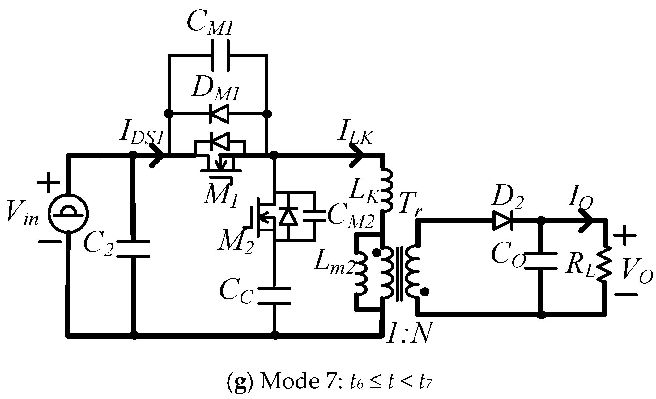
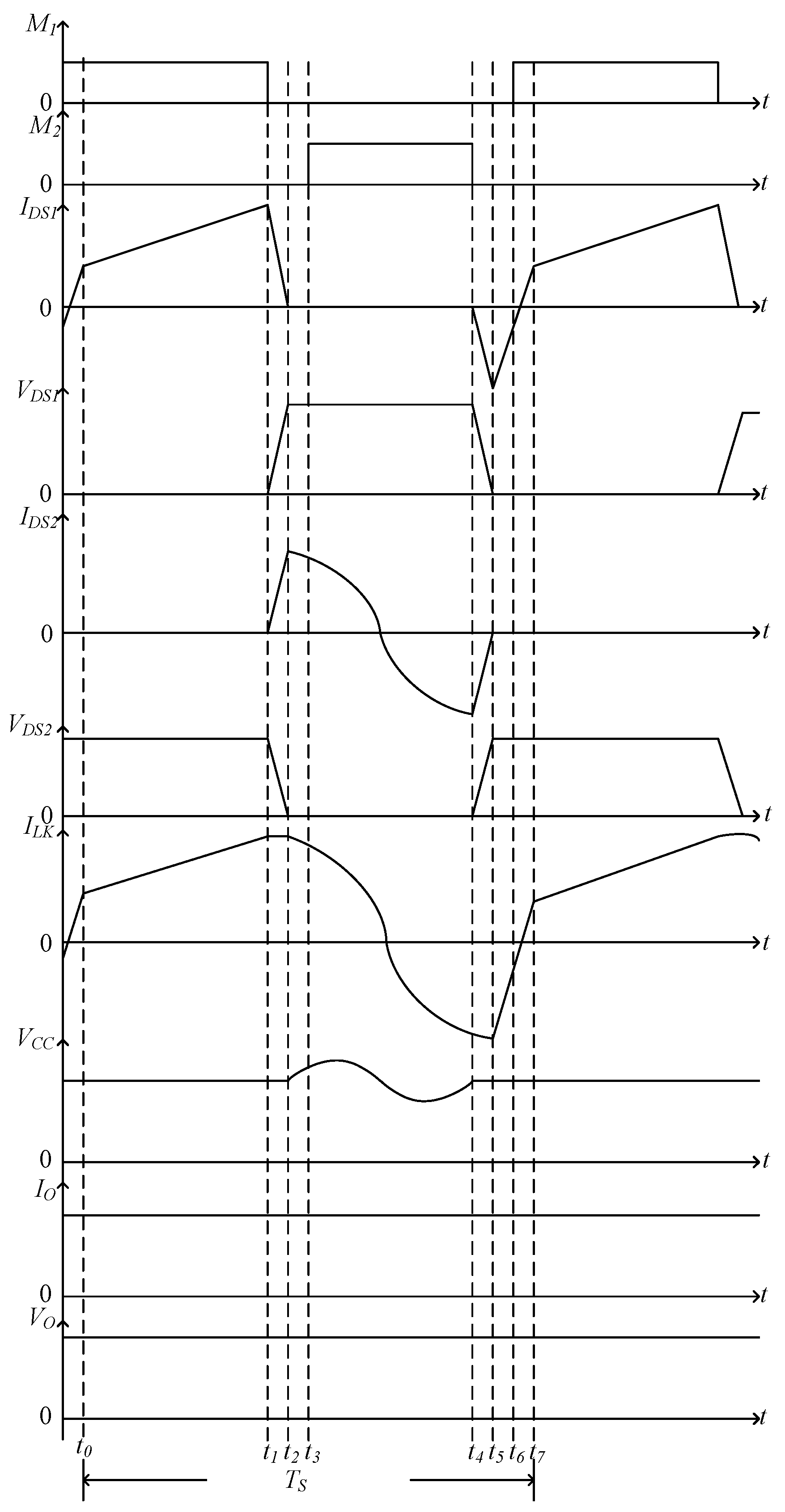
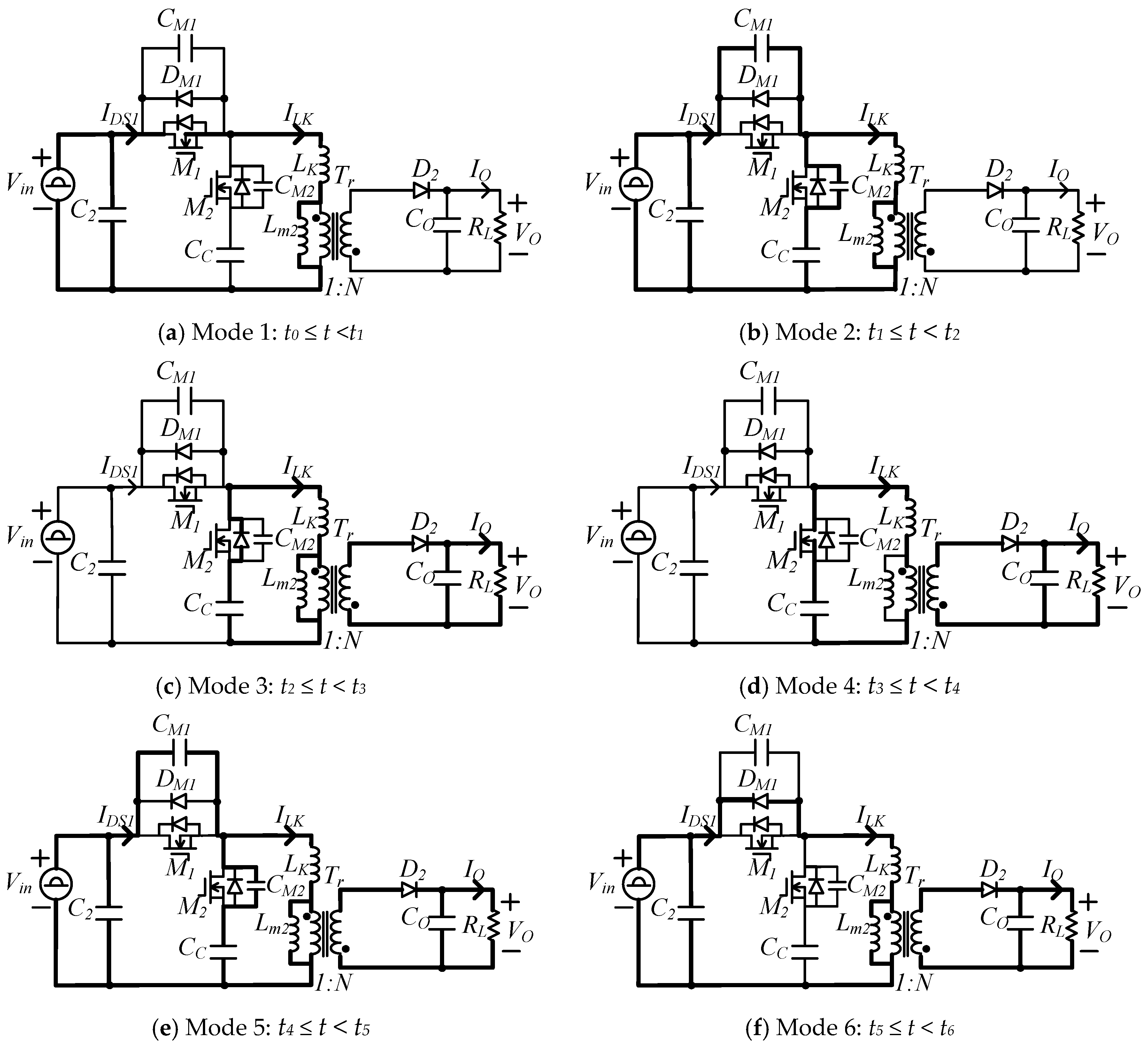
Ts. Therefore, the operational principle of the proposed bridgeless flyback converter can adopt, that input voltage is a constant DC voltage and the proposed one is operated in the positive half period of the line source, to explain its operational principle. According to the operational principle of the proposed converter, operational modes of the proposed one are divided into seven modes. Each operational mode is shown in
Figure 12 over one switching cycle, and its key waveforms are illustrated in
Figure 13. Its operational principle is described in the following.
Mode 1 [
Figure 12a;
t0 ≤
t <
t1]: Before
t0, switch
M1 is kept in the turn-on state, while
M2 is in the turn-off state. When
t =
t0, current
IDS1 of switch
M1 reaches to the initial current which is the minimum inductor current
IL(0) of the proposed converter operated in continuous conduction mode (CCM). Within this time interval, the inductor current
ILK linearly increases and current
IDS1 is equal to
ILK. Since the diode
D2 is reverse biased, the capacitor
Co supplies the load with energy. In this interval, inductance
Lm1 is in the stored energy state.
Mode 2 [
Figure 12b;
t1 ≤
t <
t2]: At
t =
t1, switch
M1 is turned off and
M2 is operated in the off state. The energies stored in leakage inductor
Lk and magnetizing inductor
Lm1 are transferred to capacitors
CM1 and
CM2. Voltage
VDS1 across switch
M1 is charged from 0V to (
Vin +
Vo/
N) and voltage
VDS2 across switch
M2 is charged from (
Vin +
Vo/
N) to 0 V. Since the charge time is very small, capacitor
CM1 is in an approximately linear charging state and
CM2 is in an approximately linear discharging state. The output capacitor
Co maintains output voltage
Vo at a desired value.
Mode 3 [
Figure 12c;
t2 ≤
t <
t3]: When
t =
t2, switch voltage
VDS1 is equal to (
Vin +
Vo/
N) and
VDS2 equals to 0 V. Diode
D2 and
DM2 starts to forwardly bias. Voltage of secondary winding in transformer
Tr is clamped to output voltage
Vo. Within this time interval, inductance
Lk and capacitor
Cc are in a resonant manner. Furthermore, magnetizing inductor
Lm1 releases the energy through transformer
Tr to load.
Mode 4 [
Figure 12d;
t3 ≤
t <
t4]: At
t3, switch
M2 is turned on and switch
M1 is kept in the off state. Since the body diode
DM2 is forward biased before switch
M2 is turned on, switch
M2 is operated with ZVS at turn-on transition. Inductance
Lk and capacitor
Cc are kept in the resonant state. The energy stored in
Lm1 is transferred to load by means of transformer
Tr.
Mode 5 [
Figure 12e;
t4 ≤
t <
t5]: When
t =
t4, switch
M2 is turned off. A new resonant network is formed between inductance
Lk and capacitors
CM1 and
CM2. Capacitor
CM1 is discharged and
CM2 is charged through inductance
Lk. As a sequence, switch voltage
VDS2 changes from 0 V to (
Vin +
Vo/
N), while
VDS1 varies from (
Vin +
Vo/
N) to 0 V. Magnetizing inductance
Lm1 is in the released energy state. Diode
D2 maintains in the forwardly bias state.
Mode 6 [
Figure 12f;
t5 ≤
t <
t6]: At
t5, switch voltage
VDS1 is equal to 0 V. Inductance current
ILk equals a negative value. Voltage across inductance
Lk is equal to (
Vin +
Vo/
N). The operational states of magnetizing inductance
Lm1 and diode
D2 are the same as those states of mode 5.
Mode 7 [
Figure 12g;
t6 ≤
t <
t7]: When
t =
t6, switch
M1 is turned on. Since body diode
DM1 is forward biased before
t =
t6, switch
M1 is operated with ZVS at turn-on transition. Inductance current
ILk varies from a negative value to the initial current which is the minimum current value of inductance
Lm1 when the proposed converter is operated in CCM. When
t =
t7, current of magnetizing inductance
Lm1 reaches its minimum value again, a new switching cycle will start.
4. Design of the Proposed PFC
Due to the input voltage with a sine wave, the input current
Iin is time dependent. A function of peak current of switch
M1 or
M2 is, in turn, a function of duty cycle of the converter. Therefore, peak switch current
IDS1 needs to be determined as a function of which the instantaneous operating point is on the input line period. Neglecting ripple current in the switch, switch current
IDS1(
ϕ) can be determined by
where
Iav(
ϕ) is the average input line current and
D(ϕ) is an instantaneous duty cycle. In (1), one half of the line cycle period is considered to be normalized to the interval [0, π], and
ϕ is an arbitrary point on that interval.
Iav(
ϕ) is given by
where
Po is the output power of the converter,
indicates the conversion efficiency and
Vrms is the input voltage of line source. The instantaneous duty cycle is
where
Vo is the output voltage and
N is the turns ratio of transformer
Tr. As mentioned above,
D(ϕ) can vary from
Dmin to 1. In order to achieve systematic design of the proposed bridgeless flyback converter, its design is listed as follows:
● switches M1–M2
The turns ratio
N of transformer is selected to accommodate a low voltage ratio device for minimum duty cycle of switch to realize reasonable values, when the active clamp circuit in the proposed converter can provide a perfect suppression of the spike voltage across the main switch
M1 or
M3 due to leakage inductance of transformer, the maximum off-state voltage
VDS1(max) can be determined by
where
is the high line voltage of input source which is equal to AC 265 V and
Vo indicates the output voltage. The ranges of the minimum duty cycle can be given by
And
where
is the low line voltage of the input source which is equal to AC 90 V. In general, the minimum duty cycle ranges are determined between 0.2 and 0.5 under the input source at high line or low line voltage.
The maximum switch average current
occurs at the maximum load and the minimum line voltage, when power factor is approximately unity, the maximum switch average current
is written by
where
is output power of the proposed converter operated in the full load condition. Its worst case maximum peak current also occurs under the same operating conditions as above. The peak current
can be calculated from
where
Lm is the magnetizing inductance of transformer
Tr and
TS is the switching period of switch
M1 or
M3. For this particular design, since voltage stress and peak current of active clamp switch
M2 or
M4 are the same as that of switch
M1 or
M3, device selection of switch
M2 or
M4 is the same as
M1 or
M3.● Transformer Tr
Since input voltage changes from a low line voltage
to a high line voltage
, it will affect the minimum duty cycle
and
. In order to obtain a reasonable value of
or
for active clamp flyback converter,
or
is designed at between 0.3 and 0.5. According to the reasonable ranges of
or
, turns ratio
N is determined by
Or
The input voltage
Vin adopts a sine wave. During the positive half period or the negative half period, input voltage
Vin can vary from 0 V to the maximum value, and then from the maximum value to 0 V. In order to determine magnetizing inductance
Lm1(=
Lm) or
Lm2(=
Lm), current variation value △
ILm of magnetizing inductance
Lm1 or
Lm2 is determined with the worst case maximum peak switch current as a reference value. Therefore, △
ILm can be written by
For this particular design, K is determined at approximately 0.1.
● Clamp Capacitor CC
Since switches
M1–
M4 are operated with ZVS at turn-on transition and the energy stored in leakage inductance
LK can be recycled, it is by means of leakage inductance
LK and clamp capacitor
CC operated in the resonant manner. A better design of the proposed converter is to select the clamp capacitor
CC value so that one half of the resonant period formed by the clamp capacitor
CC and leakage inductance
LK exceeds the maximum off time of switch
M1 or
M3. Therefore, clamp capacitor
CC can be determined by
where
LK is equal to 1~5% of magnetizing inductance
Lm1 or
Lm2.
● Output Capacitor Co
The output capacitor
Co is used to reduce output voltage ripple. Since the input voltage
Vin of the proposed converter is a half-wave rectification waveform, output voltage
Vo contains a voltage ripple with 120 Hz. When the maximum peak output voltage △
Vo is specified, output capacitor
Co can be given by
where
(=
) is the maximum output power. Furthermore, the required ripple current rating
for output capacitor is determined by
5. Measured Results
In order to verify performances of the proposed power system, as shown in
Figure 8, a prototype with following specifications was implemented. The proposed power system includes two converters: The DC/DC converter with battery source and the proposed PFC with line source. Their specifications are respectively shown in the following:
The DC/DC converter with battery source
Input Voltage VB: DC 20–26 V (two batteries connected in series),
Switching frequency fs: 50 kHz,
Output Voltage VDC1: DC 48 V,
Maximum output current IDC1(max): 2.5 A, and
Maximum output power PDC1(max): 120 W,
The proposed PFC with line source
Input voltage Vin: AC 90–265 V,
Switching frequency fs: 50 kHz,
Output Voltage VDC2: DC 50 V,
Maximum output current IDC2(max): 6 A,
Maximum output power PDC2(max): 300 W,
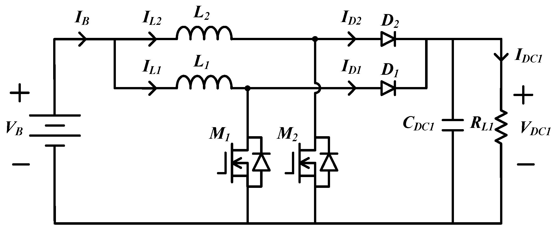
According to the previous specifications, the design values of the key components of the proposed power system can be determined. The DC/DC converter with battery source is shown in
Figure 14 and the proposed PFC with line source is shown in
Figure 6. According to design of the proposed flyback converter, parameter values in the proposed one is listed in
Table 3. Semiconductor selection of the proposed one is illustrated in
Table 4. Their devices are determined as follows:
The DC/DC converter with battery source
Switches M1, M2: IRFP250,
Diodes D1, D2: SR10100,
Inductances L1, L2: 230 μH, and
Capacitor CDC1: 1000 μF,
The proposed PFC with line source
Switches M1–M4: IRG4PH50KDPbF,
Transformer Tr core: EE-55,
Diode D2: 40EPF06PbF,
Output capacitor CO: 2200 μF/63 V
Diodes D1, D3: HFA08TB60,
Capacitors C1, C2: 0.1 μF/630 V,
Clamp capacitor CC: 0.47 μF,
Turns ratio N of transformer Tr: 0.5,
DLLmin: 0.43, and
Magnetizing inductances Lm1, Lm2: 2.72 mH,
Since this paper focuses on design and implementation of the bridgeless flyback converter, measured results of the DC/DC converter with battery source have only shown that output voltage
VDC1 and current
IDC1 under step-load changes and under supplying power to load in parallel connection. Measured output voltage
VDC1 and current
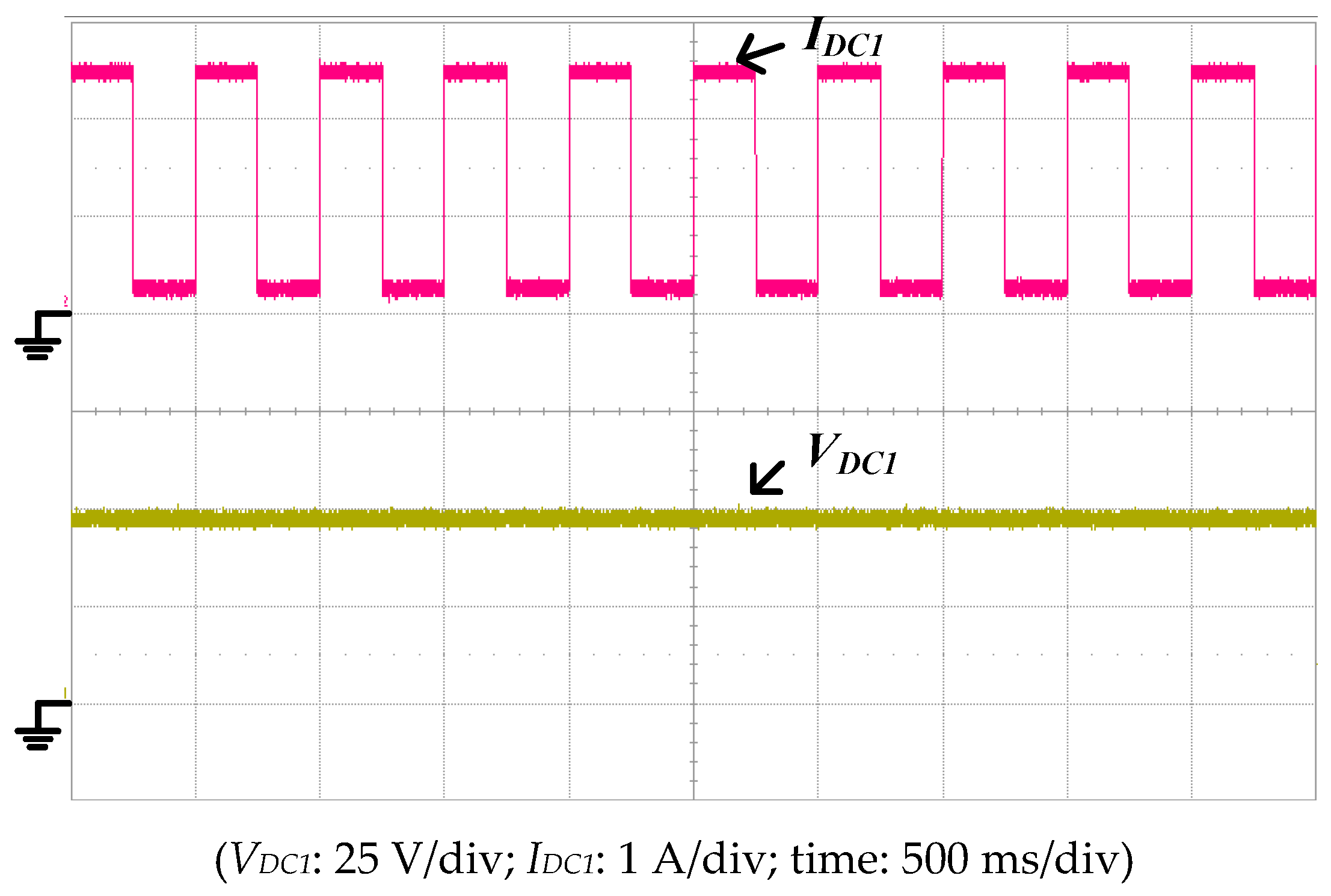
IDC1 waveforms under step-load changes between 10% and 100% of full load condition with duty ratio of 50% and repetitive period of 1s is shown in
Figure 15. From
Figure 15, it can be seen that the voltage regulation of output voltage
VDC1 has been limited within ±1%.
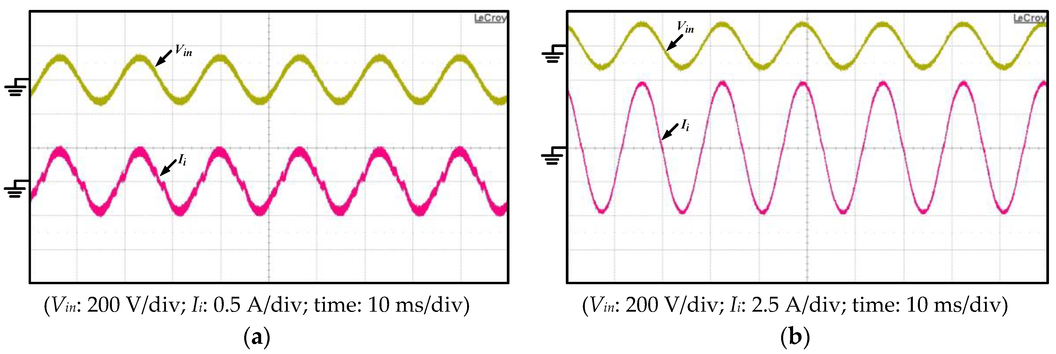
For the proposed PFC, since the input voltage
Vin of AC 90 V is the worst case for operational states of the proposed one, the experimental results are shown with the input voltage of AC 90 V. Measured waveforms of input voltage
Vin and current
Ii is shown in
Figure 16 under the line source of AC 90 V.
Figure 16a shows those waveforms under 10% of full load condition and
Figure 16b illustrates those waveforms under 100% of full load condition. From
Figure 16, it can be found that input voltage
Vin and current
Ii are approximately in phase.
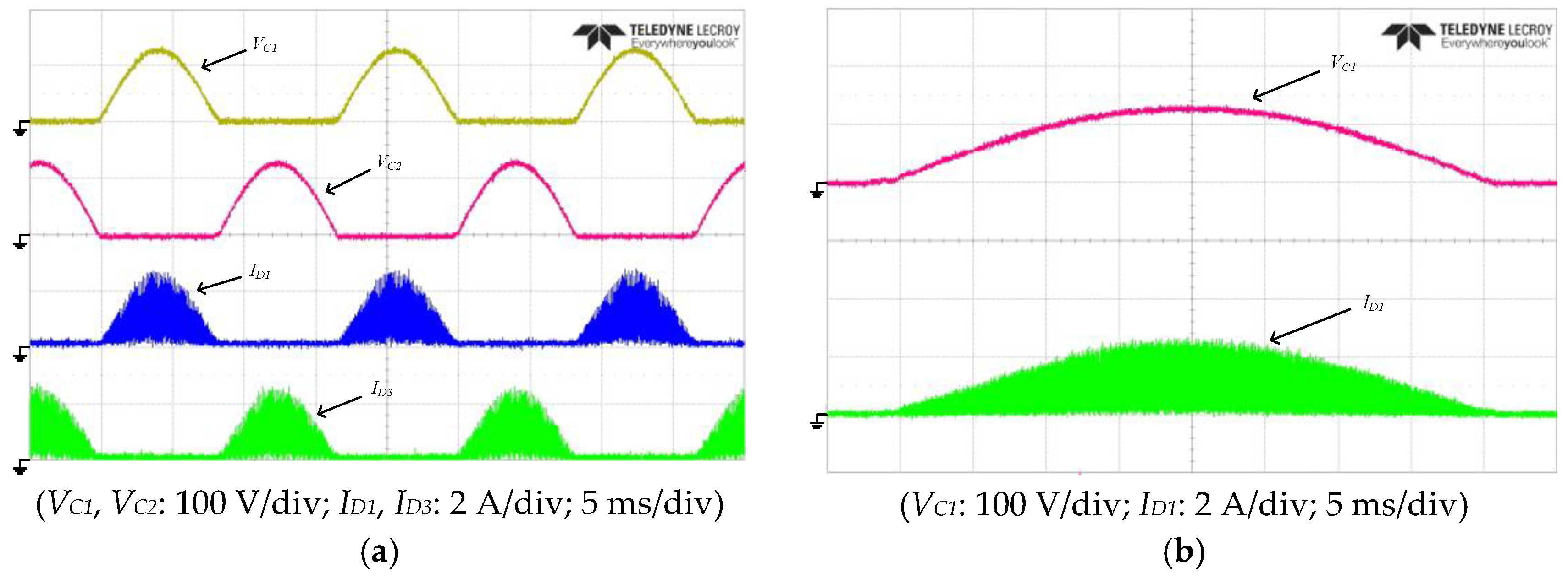
Figure 17a illustrates measured waveforms of voltages
VC1,
VC2 and currents
ID1,
ID3 under 50% of full load condition and the input voltage of 90 V, while
Figure 17b shows measured waveforms of voltage
VC1 and current
ID1. From
Figure 17, it can be seen that waveforms of currents
ID1 and
ID3 follow ones of voltages
VC1 and
VC2 variation, respectively. Since duty ratio
D varies from 0.204 to 1, and the proposed flyback converter is operated in DCM or CCM.
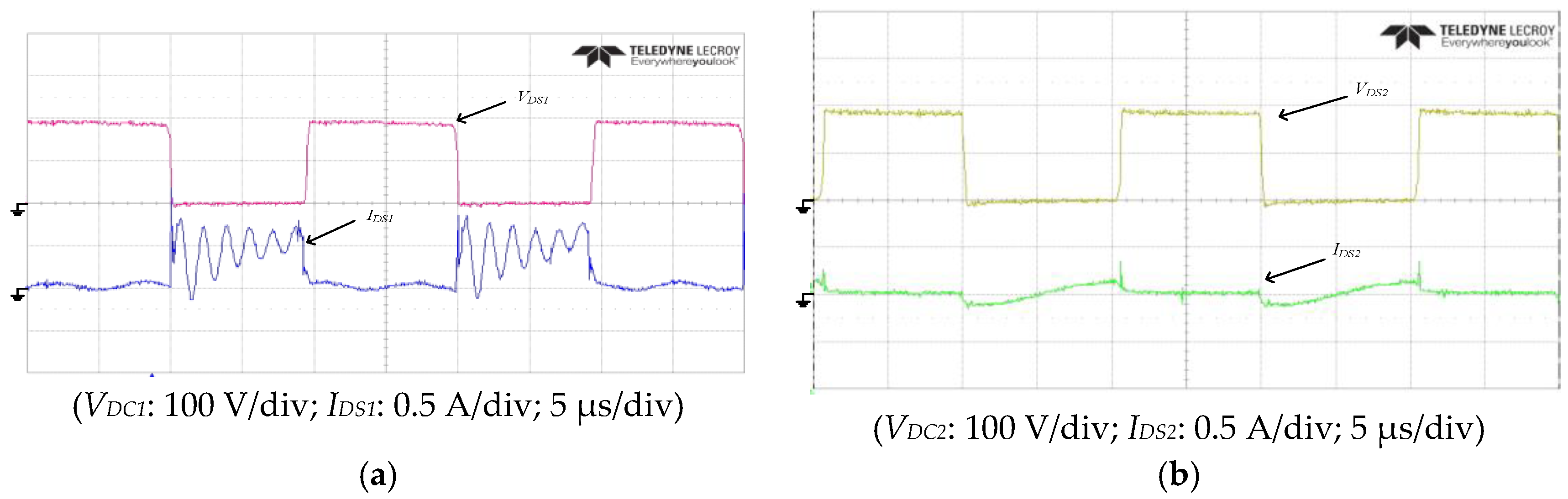
Figure 18 and
Figure 19 show measured waveforms of switch voltage
VDS and current
IDS under input voltage of 90 V.
Figure 18 illustrates measured waveforms of switch voltage
VDS1 and current
IDS1, and switch voltage
VDS2 and current
IDS2 and current
IDS2 under 10% of full load condition and the input voltage of 90 V. From
Figure 18, it can be found that the proposed flyback converter is operated in DCM. The active clamp capacitor can reduce the voltage spike and recover energy stored in leakage inductor of the transformer.
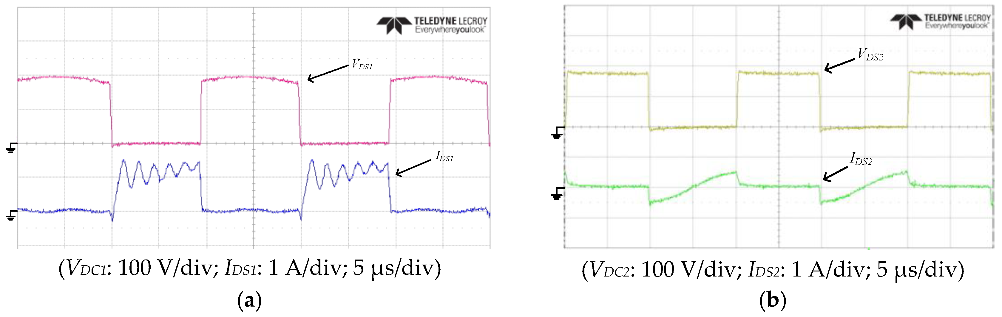
Figure 19 depicts those waveforms under 30% of full load condition and the input voltage of 90 V, from which it can be seen that switches
M1 and
M2 are operated in ZVS at turn-on transition. In
Figure 18 and
Figure 19, voltage
VDS1 across switch
M1 has a ring voltage. The ring voltage is generated by leakage inductor of secondary winding of transformer and parasitic capacitor of diode
D2 when switch
M1 is turned on. It can be eliminated by snubber circuit applied to diode
D2.
Measured output voltage
VDC2 and current
IDC2 waveforms under step-load changes between 10% and 100% of full load condition with duty ratio of 50% and repetitive period of 1s as shown in
Figure 20, from which it can be observed that the voltage regulation of output voltage
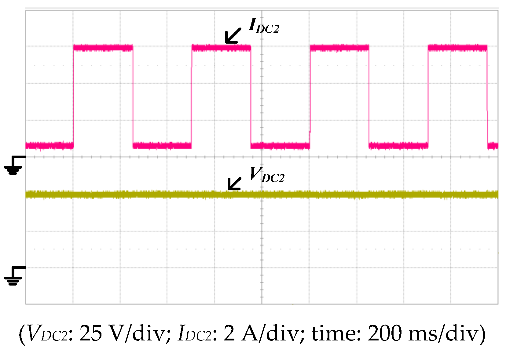
VDC2 has been limited within ±1%.
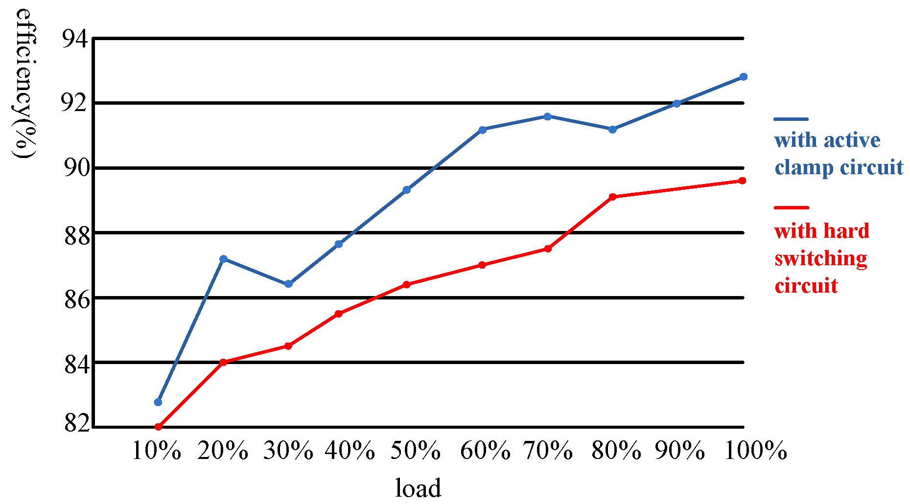
Figure 21 depicts the measured efficiency of the proposed PFC from light load to heavy load under AC 90 V. When load is greater than 40% of full load condition, each efficiency is greater than 86%. For further increase in conversion efficiency of the proposed converter, switches
M1–
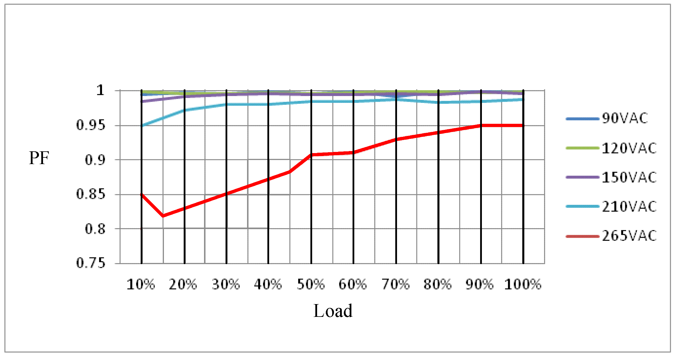
M4 can adopt a lower conduction resistance to reduce conduction loss. It also decreases the switching frequency of the switch to reduce switching loss. In order to verify a high PF, the plot of power factor of the proposed one from light load to heavy load illustrated in
Figure 22, from which it can be found that power factor of the proposed one can be greater than 0.8 under different input voltages. In particular, when input voltage is at a high line level and load is in the light load, PF has a lower value. Due to a lower output current
IDC2, PFC control IC is difficult to control input current
Ii, resulting in a lower PF.
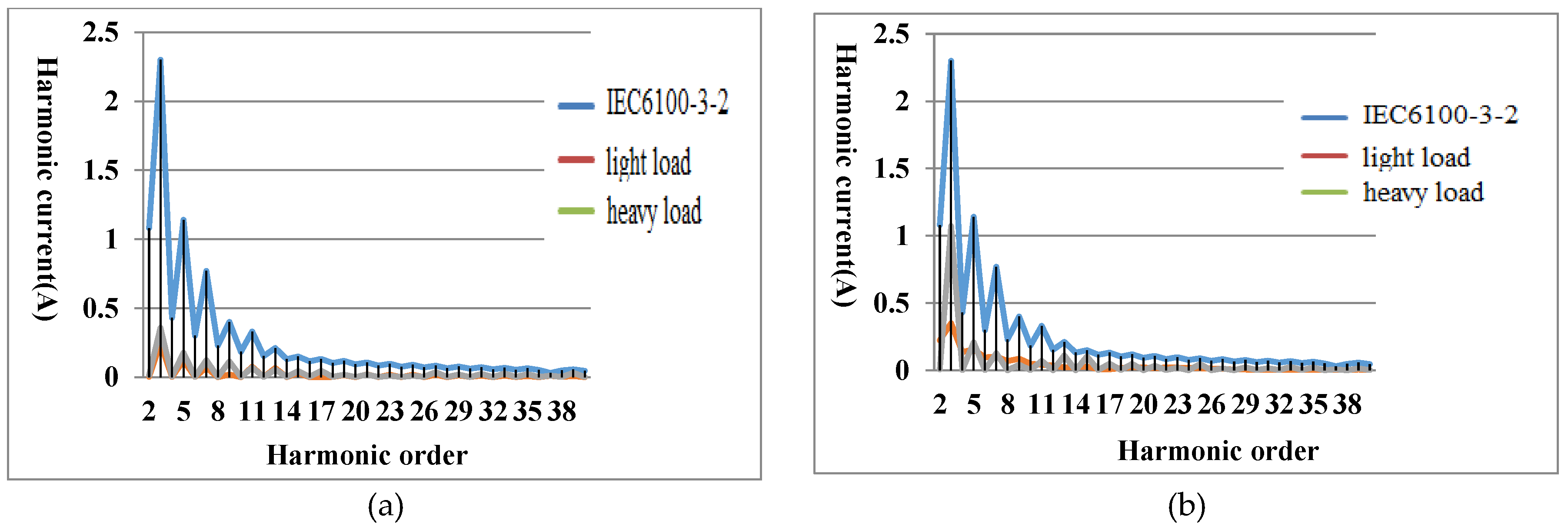
Figure 23 shows the harmonic current from light load to heavy load under different input voltage levels, illustrating that their harmonic current can meet requirements of IEC6100-3-2 class A.
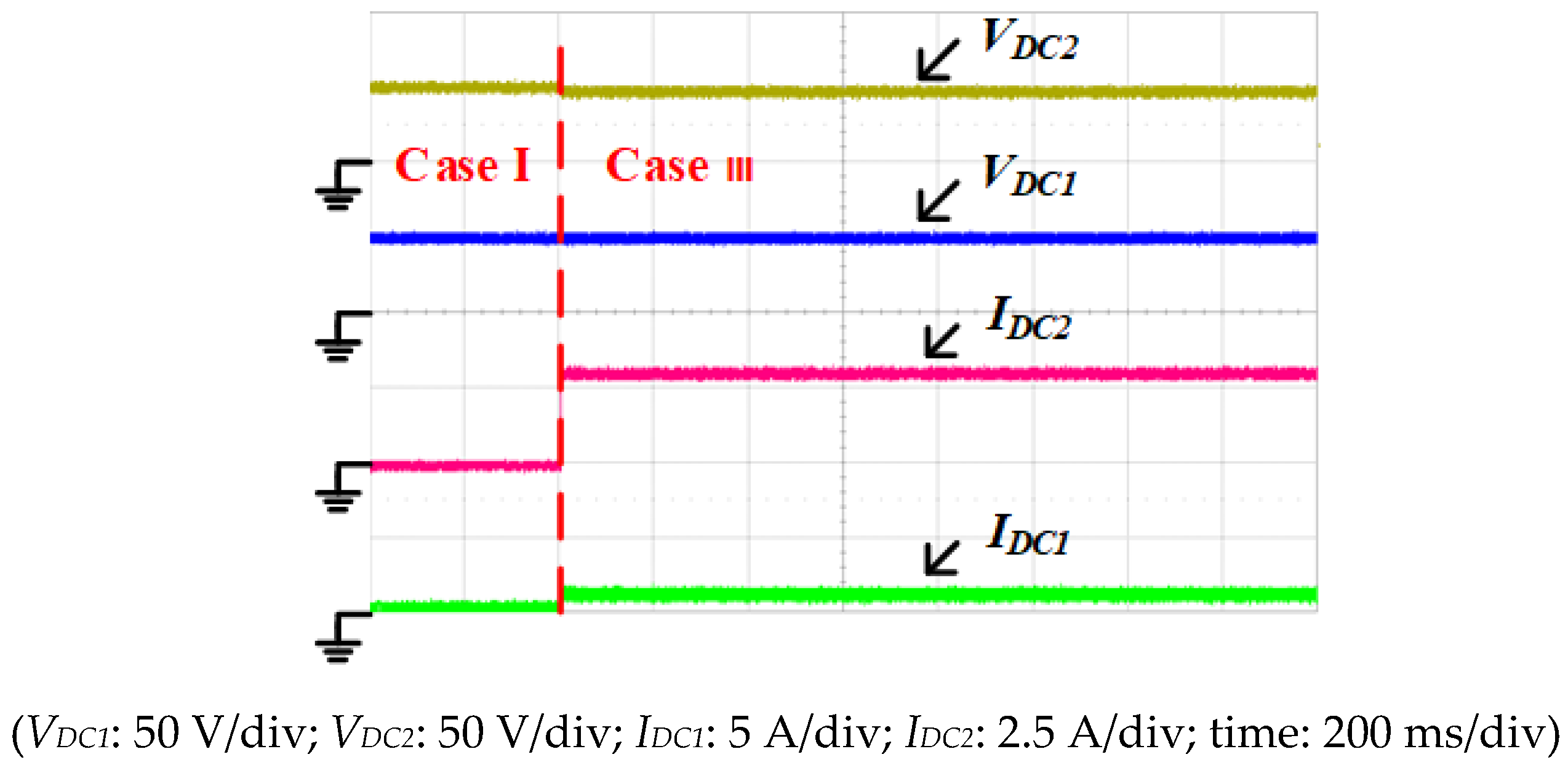
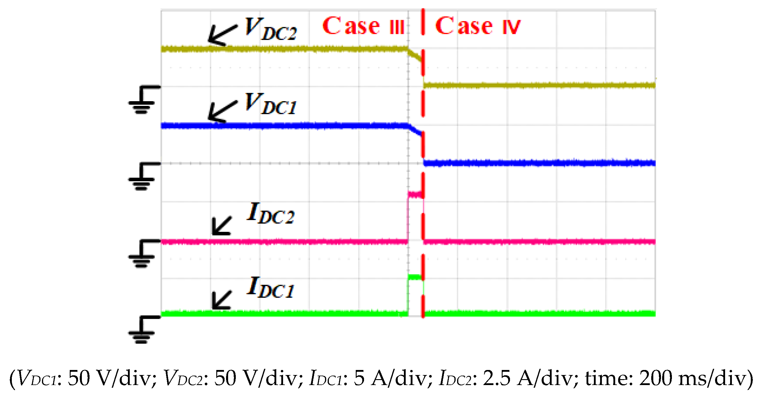
According to operational cases of the proposed power system, there are four operational cases for DC load power variations.
Figure 24 shows measured waveforms of voltages
VDC1 and
VDC2, and currents
IDC1 and
IDC2 from
PL = 0 W to
PL = 125 W. Due to
PDC2(max) = 300 W, operational case changes of the proposed one can be varied from case I to case II. When load power
PL is from 0 W to 325 W, operational case changes are from case I to case III. Those waveforms are shown in
Figure 25. If
PL variations are from 0 W to 450 W, operational case charges are from case I to case IV. Those waveforms are shown in
Figure 26. As mentioned above, the proposed power system can change operational case by the control algorithm of the proposed power system.


