1. Introduction
In the current scenario, the demand for conventional petrochemical energy resources is drastically reducing due to their scarcity in nature and the pollution caused by them. Replacement of these petrochemical energy sources with clean and renewable energy sources is the only possible solution to this problem. However, the individual use of such non-conventional energy sources, particularly renewable energy sources like solar-PV, etc., is not recommended for reliable electric power generation since their availability is highly dependent on varying climatic conditions. Hence, to achieve a highly reliable and clean electric power generation system, hybridization of such renewable and non-conventional energy sources is essential.
The Hybrid Energy System (HES) shall accommodate more than one distinct voltage-current characteristic non-conventional energy sources like solar-PV, wind, etc., and storages like a battery, ultracapacitor, fuel cell, etc. [
1,
2,
3]. A power electronic interface is mandatory to integrate these input energy sources. Parallel connected single-input DC-DC converters are widely used in the conventional scheme, and this results in substantial complexity in control strategies, increased cost, loss of compactness and system efficiency. Hence, the idea of multi-input DC-DC converters (MICs) has been introduced to surpass the demerits of conventional methods. Simple and compact structure, lower system complexity and reduced cost are the main attractive features of MICs. Compared to single-input converters, MICs can provide a reliable power supply, which is one of the potential merits of MICs [
4,
5,
6].
There are many MICs already reported in the literature [
4,
5,
6,
7,
8,
9,
10,
11,
12,
13,
14,
15,
16,
17,
18,
19,
20,
21,
22,
23,
24,
25,
26,
27]. MICs can be classified as isolated and non-isolated topologies. The cost and complexity of multi-winding transformers based isolated topologies are higher than the non-isolated topologies. A multi-input DC-DC converter based on flux additivity is introduced in [
7]. Here, the input sources are combined in the magnetic form instead of the electrical form. An efficient and generalized approach for the development of MICs is discussed in [
8,
9,
10]. A new multi-input multi-output DC-DC converter for photovoltaic and fuel cell applications is proposed in [
11]. The concept of a novel solar cell power supply system using multiple input DC-DC converters is examined in [
12]. A new MIC is introduced in [
13], which offers high voltage transfer gain. The voltage stress of the converter is low. But when the number of input increases, the number of switches and inductor increases equally. The idea of MIC to integrate different input energy sources for electric vehicle application is discussed in [
14,
15,
16,
17,
18,
19]. The detailed analysis of isolated three-port and multi-port bidirectional converter has been discussed in [
20]. The presence of the transformer to provide magnetic coupling causes the large size and complicated structure, which results in lower system efficiency and higher cost.
A novel topology for multiple energy source integration is proposed in [
21]. A dual active bridge-based isolated bidirectional DC-DC converter with proper design and control aspects is reported in [
22]. The design and control of an MIC to regulate the output voltage from different sources is proposed in [
23]. A high step-up boost converter for a solar-PV-based power generation application is presented in [
24]. The idea of implementing a suitable control strategy for a dual input DC-DC converter used in DC microgrid application is discussed in [
25]. Here, a PI control strategy is opted for the output voltage regulation, and results are validated with simulation and experimental analysis. The paper [
26] proposes a bidirectional multi input converter for fuel cell/EV application. But such converter is not suitable for renewable applications like solar-PV. The idea of decoupling the controller for a three-port DC-DC converter is discussed in [
27]. However, the idea of the independent operation of the connected inputs is not explained. An attempt is made in [
28] to explain all of the possible double-input single-output DC-DC converters using the concept of power flow graphs, which consider all of the current and voltage sources as inputs to the converter. A step-up DC-DC converter that can be extendable to n-inputs is proposed in [
29]. But, the number of energy storage elements and diodes increases when number of input increases.
The converters proposed in the literature can be utilized for the effective hybridization of the energy sources for a variety of applications. However, some of them [
4,
5] have a restriction to deliver power from the input energy sources simultaneously. Similarly, few MICs [
6,
20] have both individual and simultaneous power supply capabilities, but they have a significant number of the component count, which makes these converters unfit for higher efficiency applications. In addition to that, these converters require sophisticated control strategies for the effective integration of energy sources. Certain MICs have only unidirectional operating capacity, which makes them unfit for certain applications like hybrid vehicles, where bidirectional operational capability is a mandatory requirement. Therefore, in this paper, a novel modified bridge-type dual-input DC-DC (MBDC) converter is proposed, which has the following merits.
The proposed converter is capable of performing all three basic modes of operation such as buck, boost and buck-boost.
Both unidirectional and bidirectional power flow capability.
The ability to deliver power from the input energy sources individually and simultaneously.
Compact and simple structure.
Comparatively higher efficiency in a higher loading condition, as well.
2. Modified Bridge-Type Dual-Input DC-DC Converter
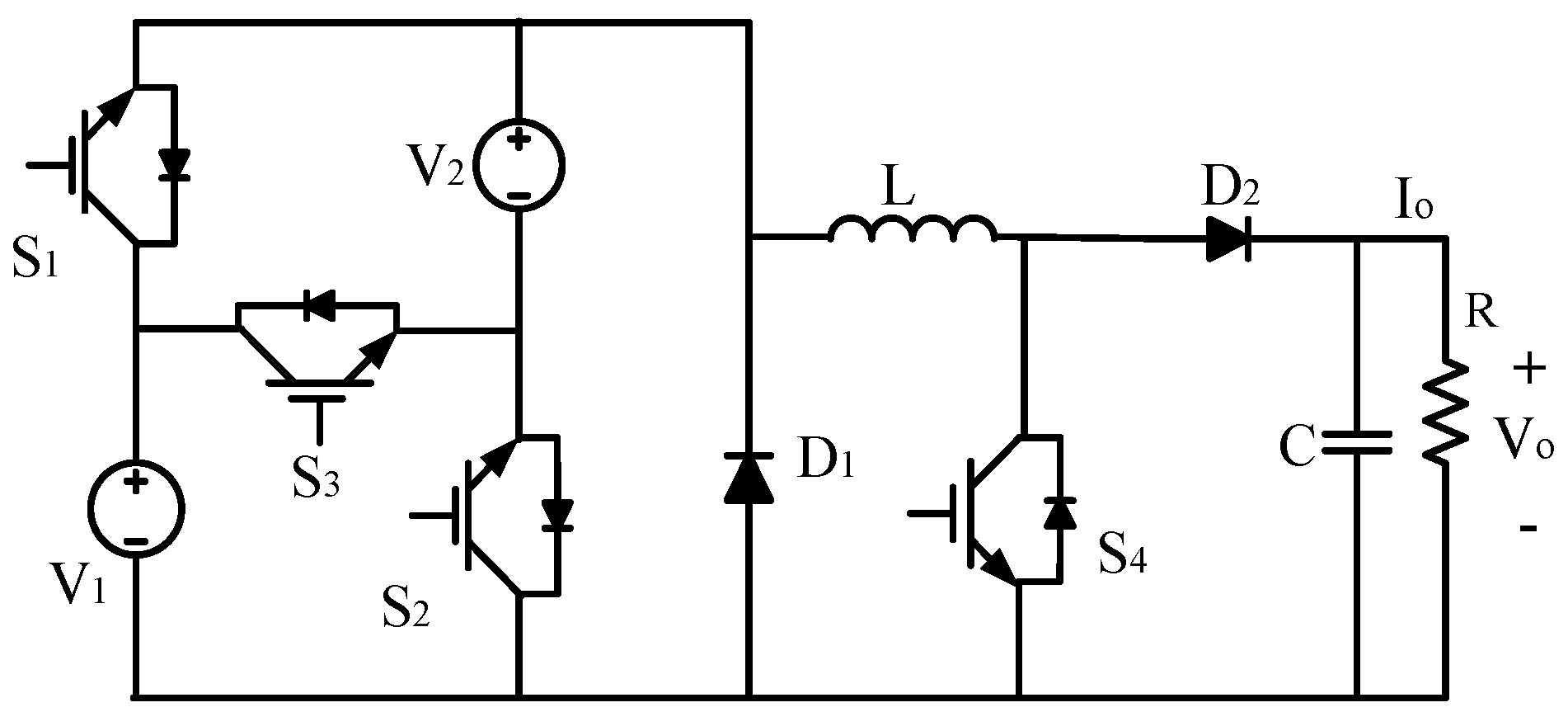
The proposed MBDC converter is derived from the traditional single-input DC-DC converter. Similar to the conventional converters, an inductor and capacitor are used to transfer energy from the source to the load. The circuit of the MBDC converter topology is illustrated in
Figure 1. Two voltage sources respectively, V
1 and V
2 are considered as input sources in this converter. Four power switches (S
1–S
4) and two diodes (D
1 and D
2) are taken into account for the unidirectional operation of the converter. If the converter needs to perform the bi-directional operation, the two diodes could be replaced by two power switches with an anti-parallel diode.
The series and parallel operation of the input sources considered in the converter are controlled by the switches S
1, S
2 and S
3. The conduction of switch S
4, diodes D
1 and D
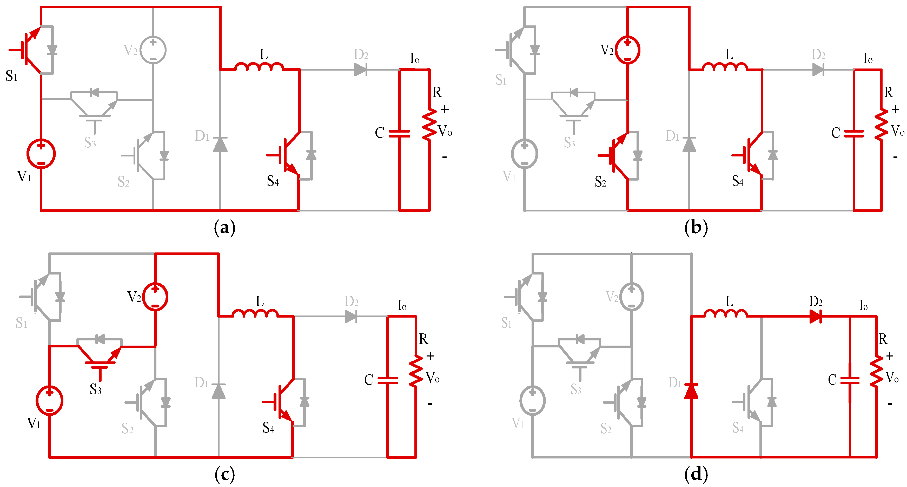
2 decides the possible operation type (buck, boost, buck-boost) and the unidirectional and bi-directional mode of the converter. All possible working states of the MBDC converter in the buck-boost type of operation are shown in
Figure 2. Based on the switching strategy of switches S
1, S
2 and S
3, there are four operating states of the converter during the buck-boost operation as given in
Figure 2a–d.
The description of the working states of the converter during buck-boost operation is given below:
- State 1:
The basic circuit diagram of State 1 is given in
Figure 2a. Here, the switches S
1 and S
4 are conducting, where the remaining switches are in the OFF condition. During this mode, the inductor is charged by the source V
1, and the capacitor delivers energy to the load.
- State 2:
The State 2 operation is illustrated in
Figure 2b. In this state, the switches S
2 and S
4 are conducting, and the remaining switches are in a non-conducting state. During this state, the inductor is charged by the source V
2, and the capacitor delivers energy to the load.
- State 3:
The circuit representation of State 3 is shown in
Figure 2c. Here, only the switches S
3 and S
4 are conducting with the remaining switches in the OFF condition. Hence, in this particular state, the storage element inductor is charged by both energy sources (V
1 + V
2).
- State 4:
Diodes D
1 and D
2 are in the forward biased condition, and other switches are in OFF condition as shown in
Figure 2d. In this case, stored energy in the inductor is discharged to the load through diodes D
1 and D
2.
2.1. Buck, Boost and Buck-Boost Operation of the MBDC Converter
The proposed MBDC converter is capable of the buck, boost, and buck-boost type of operation in both unidirectional and bidirectional ways from the source to the load. This can be achieved by a proper control of different semiconductor switches present in the MBDC converter. In the unidirectional mode, the conduction of S
1, S
2 and S
3 determines the power flow from sources, whereas the conduction of S
4, D
1 and D
2 decides the operating type of the MBDC converter (buck, boost, and buck-boost). Here, the control of switch S
3 alone is considered in the unidirectional operation of the MBDC converter. Both the input voltage sources are connected in series by turning ON switch S
3. Different types of operation of the converter associated with this case are shown in
Figure 3a–c. Similarly, this converter shall be operated additionally in three types of operation by controlling S
1 (sources V
1 alone) and three more types by controlling S
2 (sources V
2 alone). In total, nine different types of operations are possible in the MBDC converter.
Buck operation: In buck operation, when switch S
3 is ON, the inductor is charged by both the voltage sources as V
1 + V
2. When S
3 is turned OFF, the inductor discharges to the load through diodes D
1 and D
2 as shown in
Figure 3a.
Buck-boost operation: The structure of the MBDC converter in buck-boost operation is shown in
Figure 3b. During this operation, both the switches S
3 and S
4 are turned ON simultaneously, and the inductor is charged by both the voltage sources as V
1 + V
2. When the switches are turned OFF, the inductor discharges to the load through diodes D
1 and D
2.
Boost operation: The circuit diagram of the MBDC converter in boost operation is shown in
Figure 3c. Here, the switch S
3 and S
4 are turned ON together for a certain period, and the inductor is charged by both the voltage sources as V
1 + V
2. After that, switch S
4 alone is turned OFF; so that the inductor discharges to the load through diode D
2.
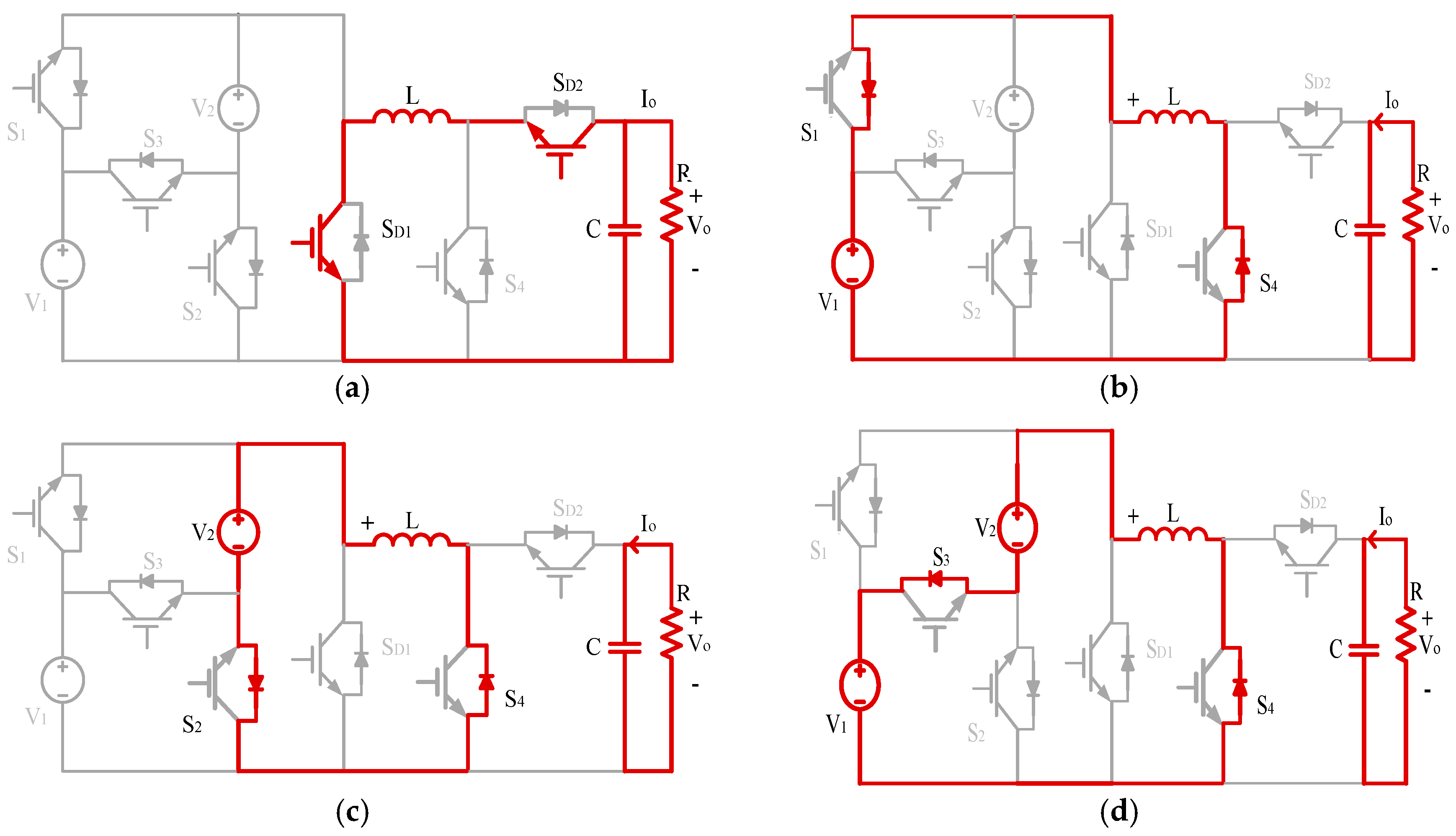
2.2. Bidirectional Operation of MBDC Converter
For storage-based sources such as battery, ultracapacitor, fuel cell, etc., it is better to adopt a multi-input DC-DC converter with bidirectional capabilities. The proposed converter can be operated in the bidirectional mode; hence, the direction of power flow can be reversed from load to source. It is required to replace each diode D
1 and D
2 by IGBT with an anti-parallel diode to operate the MBDC converter in bidirectional mode. A well-regulated voltage level can be maintained on the source side by proper control of the power switches present in the converter to ensure the better charging of the storage sources available on the input side. Different working states for the bidirectional mode of operation are shown in
Figure 4a–d. The bidirectional mode of operation of the MBDC converter is given in
Table 1.
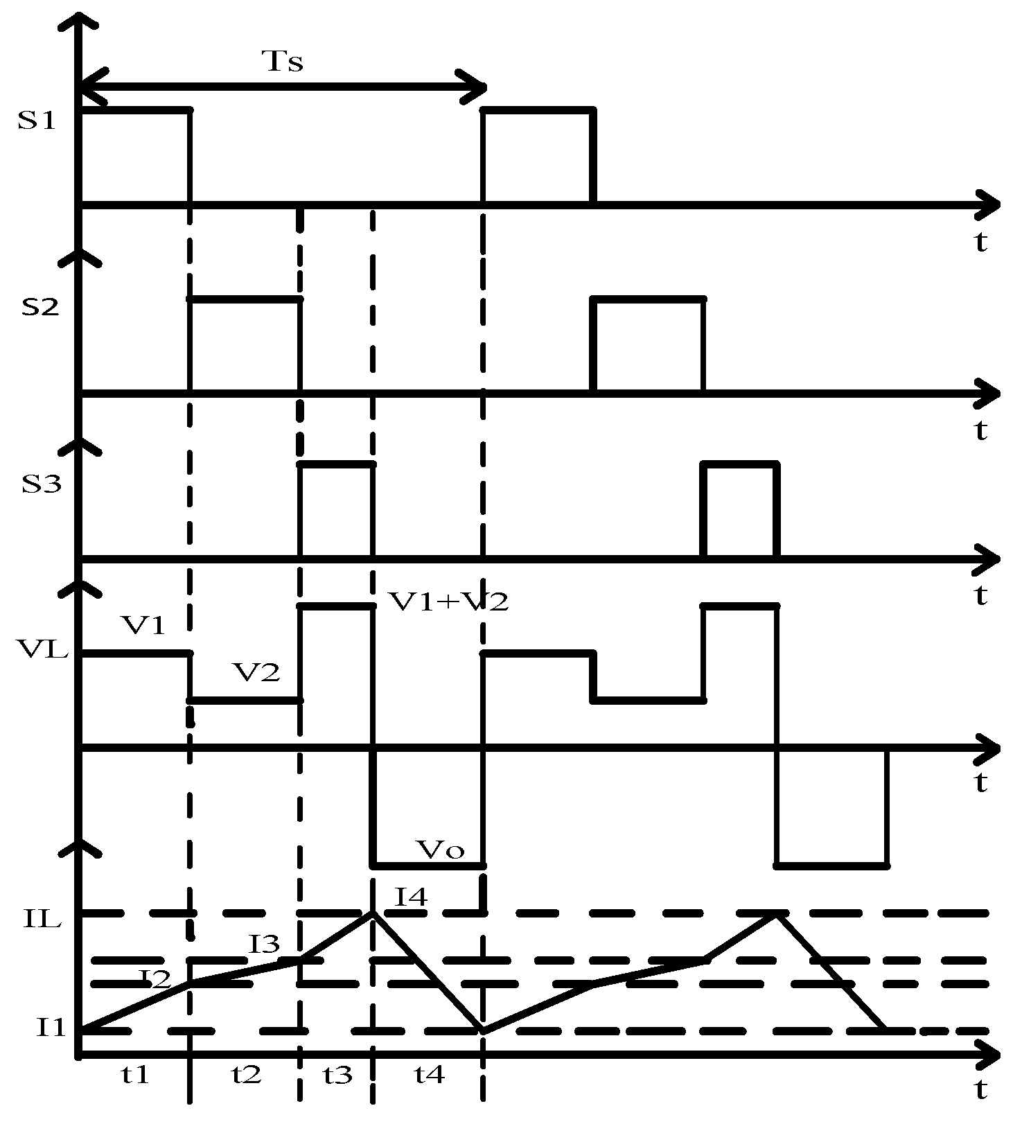
2.3. Analysis of the Converter in Unidirectional Buck-Boost Type of Operation
The analysis of MBDC converter is carried out in the continuous conduction mode (CCM) for the buck-boost type of operation.
Figure 5 shows the necessary key waveforms such as inductor voltage and inductor current of the converter during different working state over a single switching cycle.
For a DC-DC converter, the average value of the inductor voltage is zero as per the volt-second balance equation under the steady state condition as given below.
From the above equation, the output voltage of the converter is:
Input power and output power of the converter are assumed to be equal for the ideal condition as per Equation (3).
By further simplification in Equation (3), the output current is expressed as:
After substituting the value of
from Equation (2) in Equation (4),
will be:
Here, average values of and shall be expressed in terms of inductor current as , , .
By substituting the average value of source current
in terms of inductor current, Equation (6) can be derived as given below:
From Equations (2) and (6), the expression for
is obtained as:
From Equation (7) the expression for inductor current
is obtained as:
Finally, Equation (9) gives the relation between the duty ratios and source currents. Equation (9) proves that source current shall be controlled by proper tuning of duty ratios of the respective power switches.
The inductor value is calculated in terms of switching frequency, and inductor current ripple content can be expressed as:
Similarly, the value of the capacitor can be derived in terms of switching frequency and ripple content in the output voltage and is given in Equation (11).
So far, the detailed analysis of the MBDC converter in buck-boost operation is described. Similarly, the analysis of the proposed converter can be carried out in the buck and boost operations, as well. The analysis of the proposed converter in all three possible types of operations during unidirectional mode is given in
Table 2.
2.4. Voltage and Current Stress Analysis of the Switches Present in the MBDC Converter
In MICs, the selection of proper switching devices is crucial to ensure the proper operation of the converter in a cost-effective and highly-efficient manner. For this purpose, the analysis of the voltage and current stresses across the respective switching devices needs to be carried out. The maximum value of peak voltage across each switch S1, S2 is V1, V2, respectively. The value of peak voltage across switch S3 of the MBDC converter is V1 + V2, which is termed as V3. The selection of switch S4 and diodes D1 and D2 is carried out based on the voltage stress analysis of the source side switches.
The general formula for the switching stress for MBDC converter can be given as:
The analysis of the current stress of the power switches can be carried out based on the possible operating type of the converter, which is explained in the previous section. Here, the values of current stress for the power switches during buck-boost operation of the converter are considered and are given as:
The diode currents
ID1 and
ID2 are given as:
Therefore, the current stress of the switches can be expressed as:
From the analysis, it is clear that the current stress of each power switch connected to the respective sources heavily relies on the magnitude of the source voltages, whereas the current stress of the diodes depends on the magnitude of the output voltage. Based on the detailed analysis of both the voltage and current stresses of the power switches and diodes available in the converter, it is possible to choose the switching devices appropriately for better operation of the proposed MBDC converter.
2.5. Concept of Power Sharing
Based on Equation (2), it is possible to choose the different combination of duty ratios
,
and
to get a regulated output voltage,
, for the constant input voltages,
and
. Hence, the required output voltage is produced by the converter for the different combinations of the duty ratios. At the same time, different amounts of power can be delivered from the input energy sources. The possible amount of power extracted from the connected input energy sources is expressed using the following equations:
By substituting the value of
, which is expressed in Equation (8), in Equation (21), the power delivered by the sources is expressed as:
By substituting , which is expressed in Equation (2), in Equation (22), the following equations are obtained.
After simplifying the above equation, the power delivered by the sources is obtained as:
The total amount of power delivered by the input sources to the load is expressed as:
After substituting Equation (24) in Equation (25) and further simplification, the output power is obtained as:
Since
, Equation (26) can be rewritten as:
From the analysis, it is observed that the total power supplied and the output voltage are independent of the particular values of duty ratios. Hence, by the proper tuning of the power switches, the power sharing between the individual sources can be controlled.
2.6. Power Control Strategy for MBDC Converter
A multi-input converter should be capable of integrating different V-I characteristic sources with the various amounts of power extraction and provides a regulated output voltage. Hence, a suitable control mechanism is a requisite for solving the power management issues in multi-input DC-DC converters. The power control strategy may vary with the type of sources used. Therefore, it is better to design a suitable power control algorithm based on the input energy sources which considers the dynamic and steady state behavior of the connected energy sources along with the amount of power drawn.
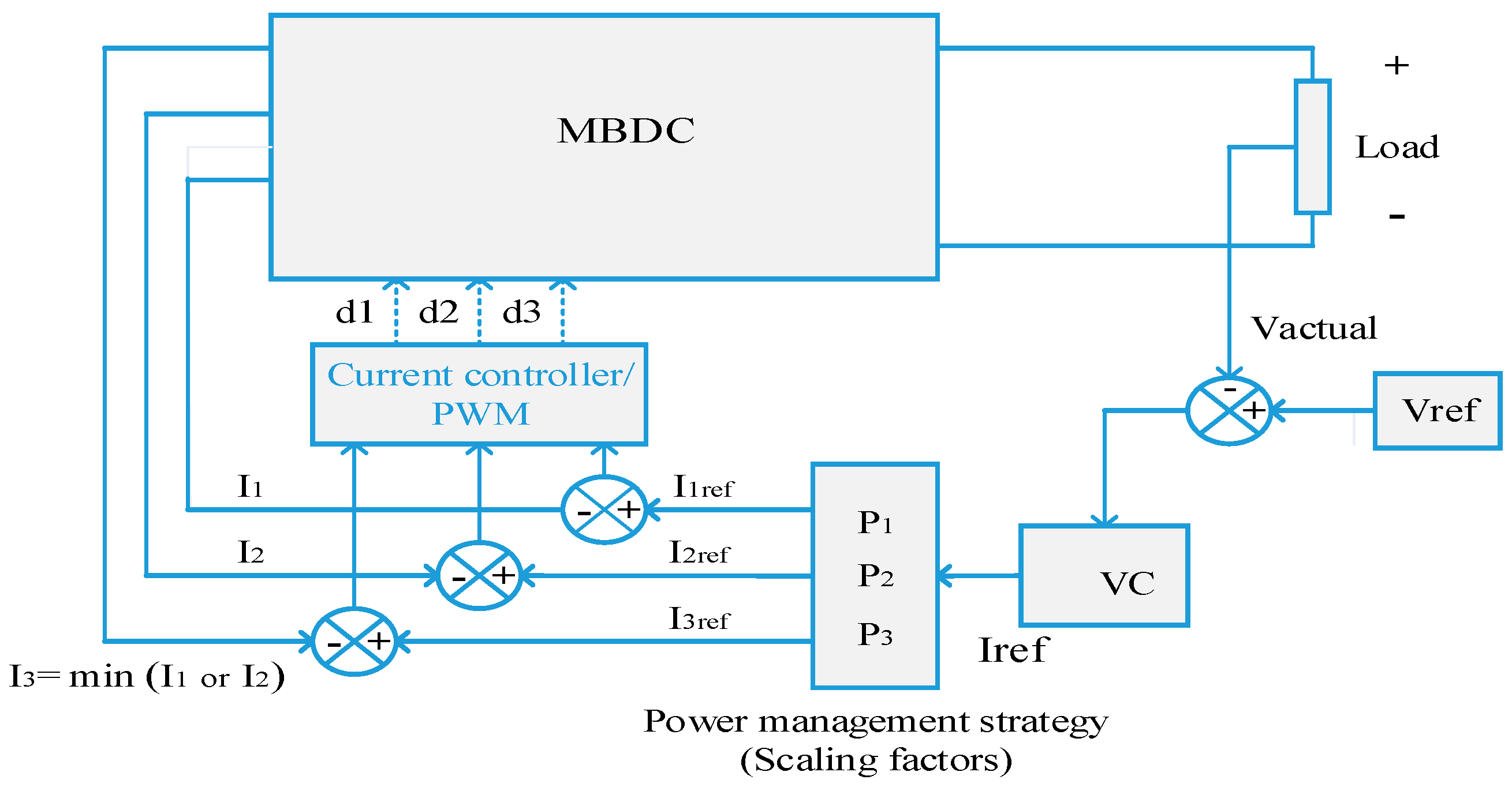
The power control algorithm should be developed based on the amount of power drawn from the connected input sources either individually or simultaneously to meet the load demand. Many control strategies are already reported in the literature. Block diagram of the power control strategy of MBDC converter is shown in
Figure 6. The control strategy is developed for regulating the output voltage during load side and source side disturbances using average Current Mode Control (ACM). In ACM two approaches are possible. One is load side control, and the other is source side control. There are certain demerits with load side control comparing to source side control. The load voltage is regulated based on the inductor current directly during the load side control. While in source side control the inductor current is indirectly controlled based on the source current to regulate the load voltage. In the first case, the requirements of sensors are less, but it offers a poor dynamic response, while the second method is appropriate for incorporating different sources with distinct V-I characteristics. Therefore, source side control is well suited for the effective utilization of the connected energy source with a good dynamic response.
In this paper, source side control is implemented. Here, the voltage at the output side is compared with the reference value, and the corresponding voltage error is applied as the input to a Voltage Controller (VC). The output of the voltage controller is the main reference current. The individual reference currents can be generated by processing the main reference current with the scaling factors derived from the input-output power relationship using a power management strategy. The scaling factors P1, P2 and P3 are considered for generating individual reference currents and can be varied between zero and one (i.e., P1 ∈ [0, 1], P2 ∈ [0, 1], P3 ∈ [0, 1]). In most of the cases, one scaling factor will be set as one, so that one connected energy source can supply the maximum available current and the remaining source can be controlled easily. In this case, the PWM pulses are generated by the current controller based on the error which is generated by comparing the actual source current with the individual reference current. Hence, during the load and source side disturbances, the regulated output voltage of the converter is obtained using this control strategy by easily controlling the duty ratios of the power switches.
Here, the implementation of the proposed control strategy has been realized by the dSPACE 1104 real-time digital controller (dSPACE GmbH, Paderborn, Germany). The LV-25P voltage sensor (LEM International SA, Plan-les-Ouates, Geneva, Switzerland) senses the output voltage of the converter, and the LA-25P Hall effect sensor (LEM International SA, Plan-les-Ouates, Geneva, Switzerland) senses the source currents. The output voltage and the source currents are fed as input to the dSPACE controller through the Analog to Digital Converter (ADC) port. These digital signals are used by the above-mentioned power control strategy, which is implemented in dSPACE. Based on the control strategy, the control signals are generated from dSPACE, and the signals are given to the power switches of the MBDC converter through the Digital to Analog Converter (DAC) port. The detailed experimental results of the closed-loop operation of the converter under load side and source side variations are given in
Section 4.
3. Simulation Results and Discussion
Open-loop and closed-loop simulation of the MBDC converter has been carried out using MATLAB/Simulink platform. Various parameters of the converter considered for the performance evaluation are shown in
Table 3. Simulation results of the MBDC converter in all three possible types of operation are depicted in
Figure 7,
Figure 8,
Figure 9 and
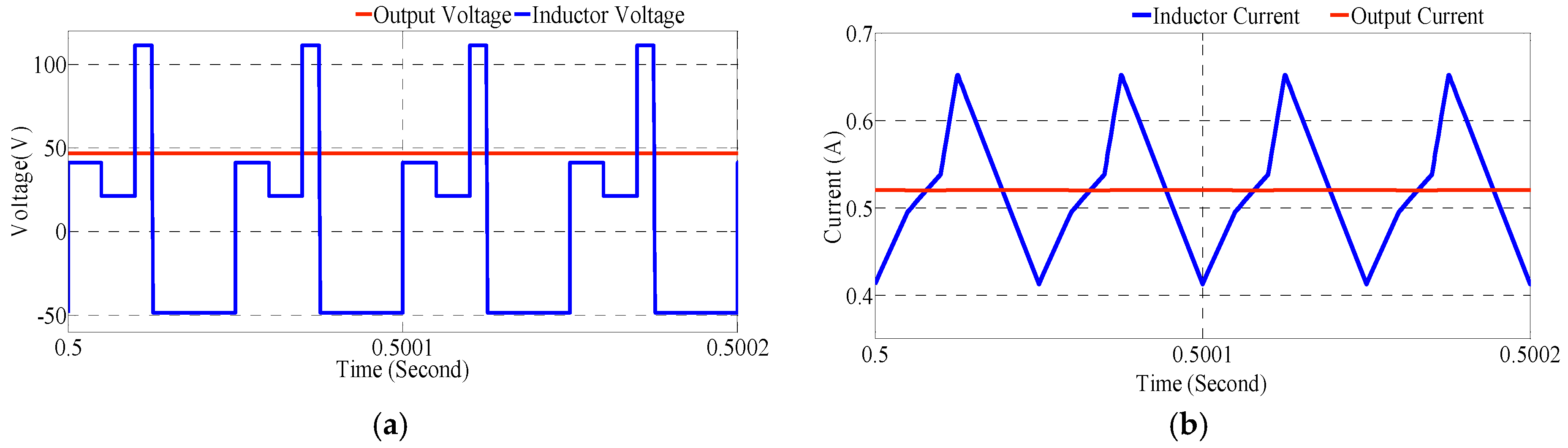
Figure 10. From
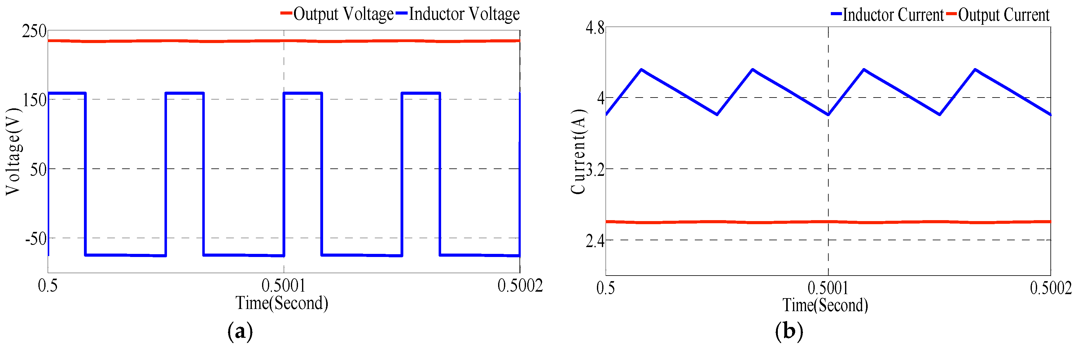
Figure 7a, it is noticed that the voltage across the inductor is 40 V (i.e., V
1 − V
0) for duty cycle
d1, and it is 20 V (i.e., V
2 − V
0) for
d2. Further, the inductor is charged by a voltage of (V
1 + V
2 − V
0), i.e., 110 V for
d3 and it is discharged with a voltage of (−V
0), i.e., −50 V, for the rest of the period.
Figure 7 shows the inductor voltage and current waveform which clearly indicates the charging and discharging process of the inductor at different working states. Therefore, by adjusting the duty cycles
d1,
d2 and
d3, inductor and load currents can be controlled. Simulation results of the proposed converter in buck-boost operation with the duty ratio (
d1 +
d2 +
d3 > 0.5) are shown in
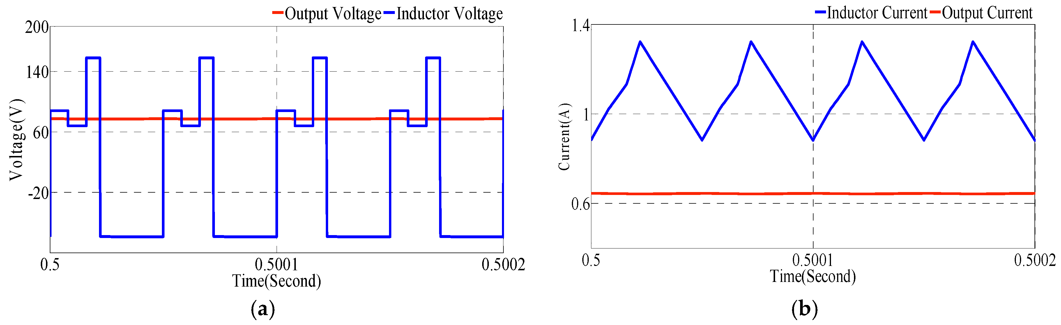
Figure 8. From
Figure 8, it is clear that, for duty cycle
d1, the voltage across the inductor is 90 V (i.e., V
1), and for duty cycle
d2 inductor voltage is 70 V (i.e., V
2). For
d3, the inductor is charged by 160 V (i.e., V
1 + V
2) and finally it is discharged by a voltage of −240 V (i.e., −V
0) for the remaining period.
Simulation results of the buck-boost operation of the converter with the duty ratio (
d1 +
d2 +
d3 < 0.5) for an output voltage of 80 V are shown in
Figure 9. Here also, for the duty ratio
d1, the inductor is charged by a voltage of 90 V (V
1), and for
d2 and
d3, it is charged by the voltage levels of 70 V (V
2) and 160 V (V
1 + V
2), respectively. Finally, it is discharged by a voltage of −80 V (i.e., −V
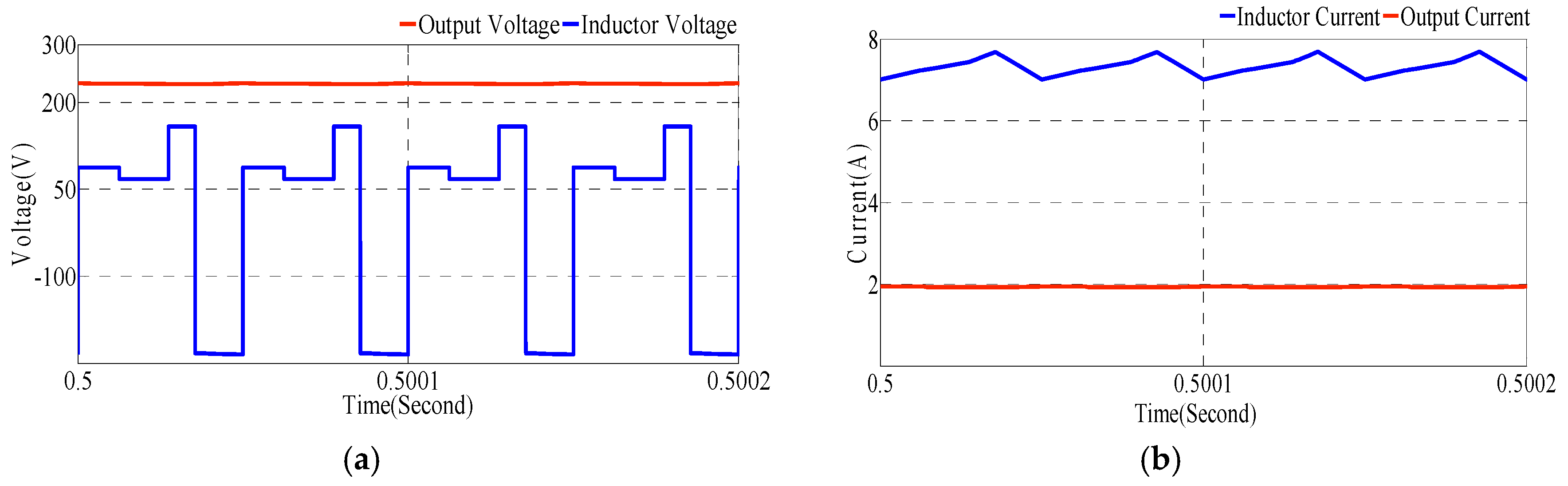
0). Simulation results of the proposed converter in boost operation are shown in
Figure 10. For the simplicity of analysis, the operation of the series switch S
3 that makes the series connection between two input energy sources V
1 and V
2 is taken into consideration. Hence, the switch S
3 is permanently turned ON, and the inductor is charged by the contribution of both sources together (i.e., V
1 + V
2), as shown in
Figure 10a. Finally, the discharging of the inductor has occurred with a voltage of −80 V (i.e., V
1 + V
2 − V
0).
4. Experimental Results
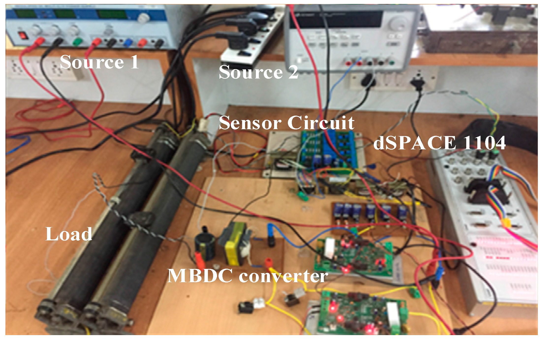
The performance and feasibility analysis of the MBDC converter have been verified in the laboratory environment using the prototype of the converter. The experimental setup of the converter is shown in
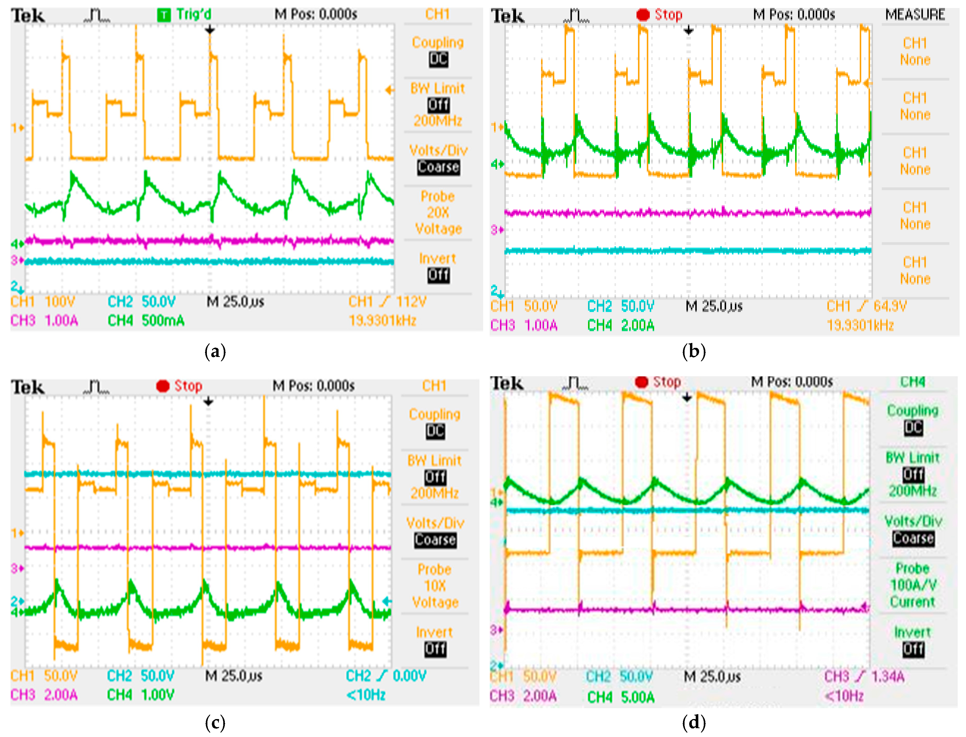
Figure 11. Two input sources with different voltage levels have been considered for the testing of the converter prototype. Here dSPACE 1104 real-time digital controller has been used for the generation of the switching pulses and real time interfacing with the converter prototype. The gate pulses for all three switches are developed with the same switching frequency of 20 kHz. In this work, the power switches for the MBDC converter are realized by FGH40N120AN IGBT switches. The experimental validation of the proposed converter is conducted for the CCM of the inductor under the steady state condition. The converter has been tested in all three types of operations: buck, buck-boost, and boost. The necessary experimental waveforms are observed using Digital Storage Oscilloscope (DSO) and the results are shown in
Figure 12a–d. The output voltage of the converter is 50 V in the case of buck operation (
Figure 12a), 80 V for buck-boost with a duty ratio <0.5 (
Figure 12b) and 240 V with a duty ratio >0.5 (
Figure 12c), as well as 240 V for boost operation (
Figure 12d).
Hence, it can be concluded that the results obtained from the experimental analysis and MATLAB simulation (R2010b, MathWorks, Natick, MA, USA) are well matched based on the waveforms shown in
Figure 7,
Figure 8,
Figure 9,
Figure 10 and
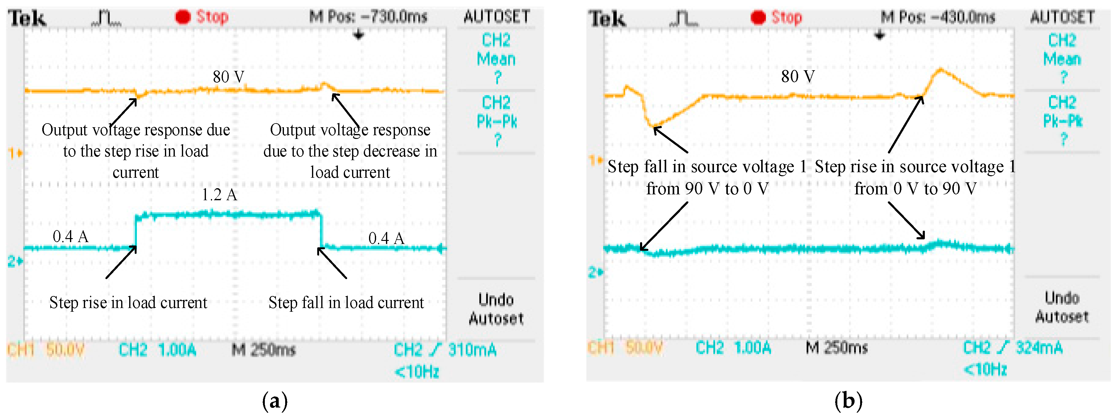
Figure 12. To observe the dynamic behavior of the MBDC converter under load side and source side disturbances, a transient analysis of the converter is conducted in the buck-boost-type of operation for a duty ratio <0.5. The output voltage and current response due to the changes in load and source values are observed and given in
Figure 13a,b. From
Figure 13a, it is observed that the output voltage of the converter is maintained at 80 V under the sudden change of load current from 0.4 A–1.2 A. Then, the output voltage is regulated at 80 V in a fast manner when the load current decreases from 1.2 A down to 0.4 A. Similarly, to verify the feasibility of the MBDC converter under the source disturbance condition, a large perturbation has been applied to one of the source voltages. Here, the perturbation has been given to the source voltage 1 (V
1) as shown in
Figure 13b.
From
Figure 13b, it is noticed that initially, the MBDC converter is operated with two sources (V
1 and V
2) for a short duration of time. Suddenly, a step change in Source 1 (V
1) is occurred (i.e., V
1 is drastically reduced to 0 V from 90 V). A small variation is noticed in the output voltage and current waveforms due to this effect. After a short duration of time, V
1 is again recovered to its initial value (i.e., a step rise in V
1 from 0 V to 90 V). From the result shown in
Figure 13b, it is observed that the output voltage and current are well settled at their desired values quickly after the small variations due to the step changes in the source 1 (i.e., V
1). Thus, the transient analysis of the MBDC converter in the experimental platform confirms the efficient operation of the controller designed.
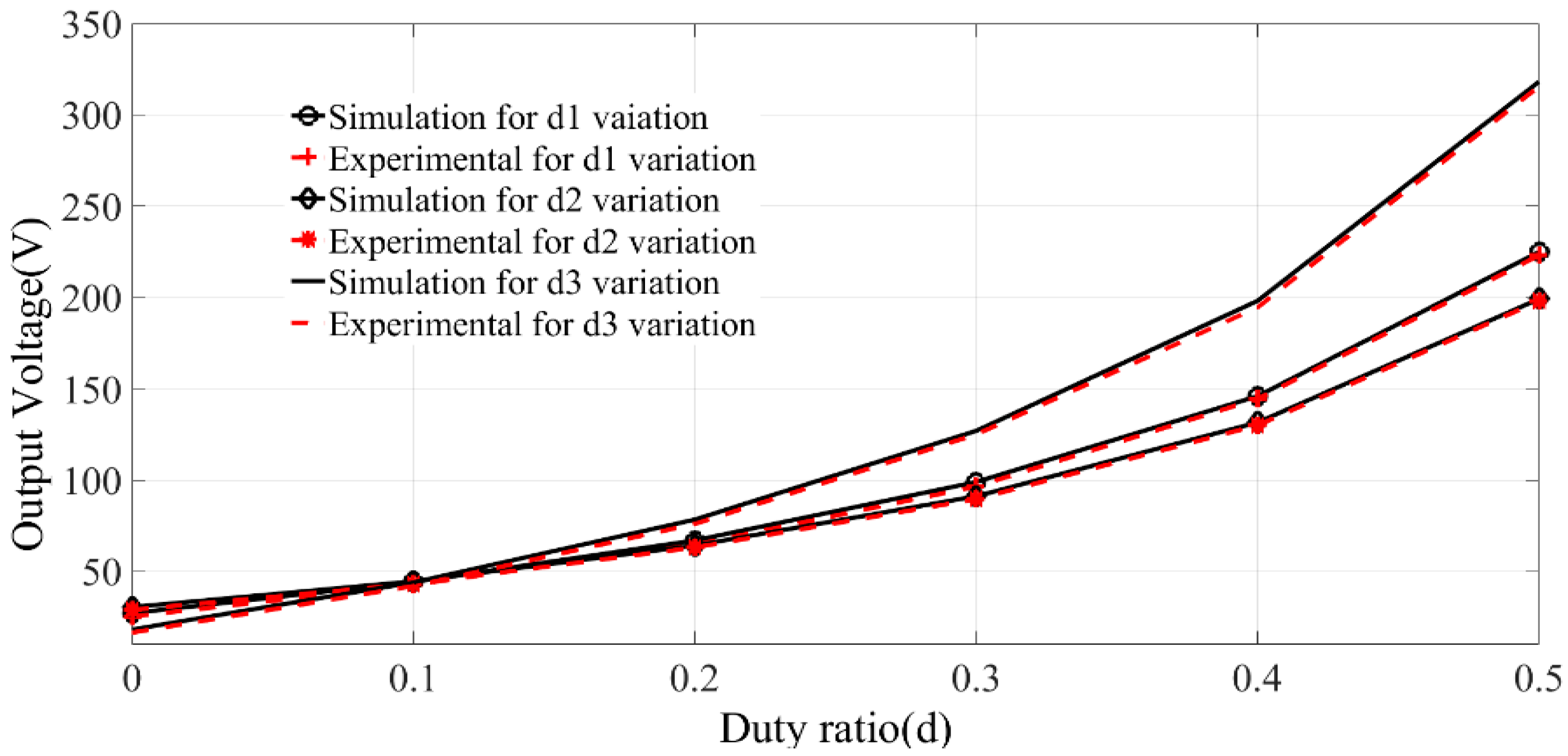
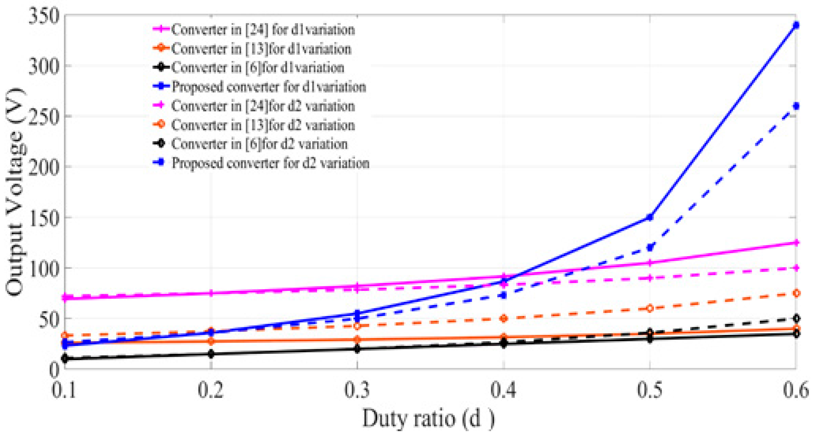
The converter output voltage due to the variation of duty ratios is observed from simulation and experimentation, and the performance comparison is shown in
Figure 14. From
Figure 14, it is noticed that the output voltage obtained from the experimental results has a slight deviation compared to the simulation results due to the non-ideal components present in the experimental prototype. Even though there is a small variation in output voltage, the MBDC converter is giving good responses in the case of experimental and simulation analysis.
A performance comparison of the MBDC converter has been carried out with three other converters proposed in the literature [
6,
13,
24]. The output voltage of the converters due to the variation in duty ratios
d1 and
d2 is analyzed in a detailed manner, and the results are given in
Figure 15. From
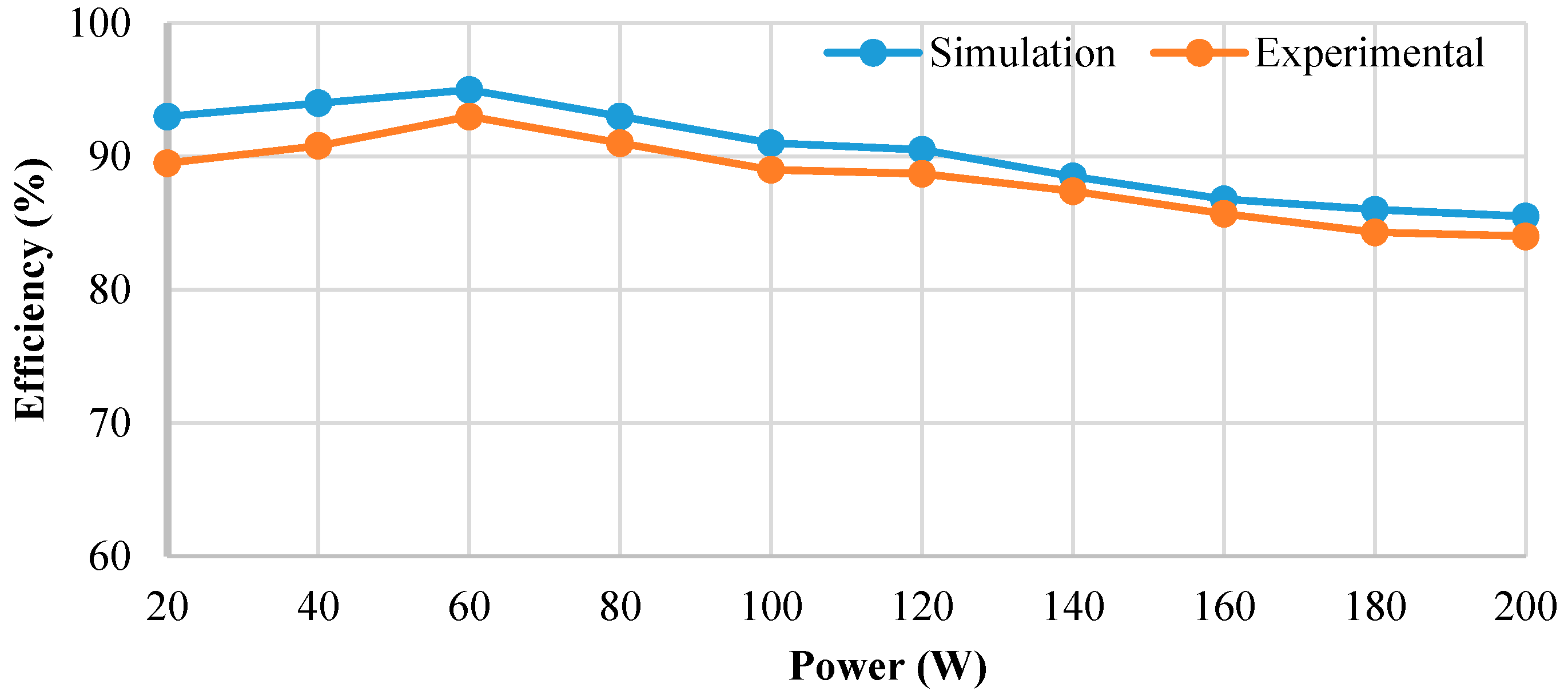
Figure 15, it is observed that the proposed converter has high output voltage gain, which enhances the importance of the MBDC converter in high voltage gain applications, compared to other MICs reported in the literature. The efficiency of the MBDC converter is evaluated under different load conditions. The value of efficiency according to the variation in output power is depicted in
Figure 16. The efficiency analysis shown in
Figure 16 clearly indicates that the proposed MBDC converter has good efficiency profile during different loading condition compared to other MICs reported in the literature. Finally, the comparison of the MBDC converter with other MICs has been carried out based on several parameters like total part counts in the converter, the efficiency and voltage stress of the converter and are illustrated in
Table 4.
5. Conclusions
A modified bridge-type two input DC-DC converter is introduced in this paper to integrate two different energy sources. The detailed analysis of the converter for all the three possible operations (buck, buck-boost, and boost) has been conducted to validate the performance of the converter. The voltage and current stress analysis of the power switches and diodes available in the converter have been performed to ensure the best and optimized selection of the switching devices in the converter. A power control strategy is developed for the MBDC converter to obtain the satisfactory response under dynamic conditions such as source and load side disturbances. The performance of the converter is carried out using the MATLAB/Simulink platform for a typical design in all three modes of operation. The converter produces the output voltage of 50 V under buck operation and 240 V under boost operation. The simulation results are satisfactory for the design of the converter. The lab-scale model of the converter is fabricated and tested successfully in the open-loop condition for the same design. The results obtained from both the simulation and experimentation are well matched with each other.
The developed power control strategy for the MBDC converter is implemented using the dSPACE real-time controller. The dynamic and steady state performance of the converter in the closed-loop condition is carried out, and the results are found satisfactory. The analysis of the converter based on the different parameters like duty ratios, efficiency, output voltage, etc., has been carried out through simulation and experimental results to validate the better performance of the MBDC converter. The proposed MBDC converter has been compared with other MICs that are already reported in the literature, based on factors such as the number of switches, inductor, capacitor, etc. The performance comparison shows that the MBDC converter is capable of operating in the buck, boost, and buck-boost modes with a lesser component count and higher efficiency. The main feature of the proposed converter is that the input sources shall be operated individually or simultaneously to supply power to the load. Hence, the MBDC converter shall be used in applications such as renewable energy integration, microgrid, aerospace, and electric vehicles.


