Article

Magnetron Sputter Epitaxy of High-Quality GaN Nanorods on Functional and Cost-Effective Templates/Substrates

Thin Film Physics Division, Department of Physics, Chemistry and Biology (IFM), Linköping University, Linköping SE-58183, Sweden
*
Author to whom correspondence should be addressed.
Energies 2017, 10(9), 1322; https://doi.org/10.3390/en10091322
Submission received: 14 July 2017 / Revised: 28 August 2017 / Accepted: 31 August 2017 / Published: 2 September 2017
(This article belongs to the Special Issue Solid State Lighting)

Abstract

:
We demonstrate the versatility of magnetron sputter epitaxy by achieving high-quality GaN nanorods on different substrate/template combinations, specifically Si, SiC, TiN/Si, ZrB2/Si, ZrB2/SiC, Mo, and Ti. Growth temperature was optimized on Si, TiN/Si, and ZrB2/Si, resulting in increased nanorod aspect ratio with temperature. All nanorods exhibit high purity and quality, proved by the strong bandedge emission recorded with cathodoluminescence spectroscopy at room temperature as well as transmission electron microscopy. These substrates/templates are affordable compared to many conventional substrates, and the direct deposition onto them eliminates cumbersome post-processing steps in device fabrication. Thus, magnetron sputter epitaxy offers an attractive alternative for simple and affordable fabrication in optoelectronic device technology.

1. Introduction

Gallium nitride (GaN) and related III-nitride semiconductor alloys represent the dominating technology in solid-state lighting (SSL) for fabrication of light-emitting diodes (LED), laser diodes (LD), and power devices [1,2,3,4]. These devices are usually fabricated on sapphire or silicon carbide (SiC) substrates. Regrettably, sapphire exhibits a large lattice mismatch (~16%) to GaN, resulting in GaN epitaxial films with a high density of dislocations. SiC, on the other hand, only has a ~3% lattice mismatch and exhibits a high thermal conductivity that simplifies device fabrication procedures but is associated with a high cost [5,6]. Alternatively, Si is an attractive substrate due to its ultra-high crystal quality, low cost, large wafer size (up to 18 inches) availability, and easy integration in integrated circuits industry. However, large mismatches in lattice and thermal expansion coefficients between Si and GaN lead to the formation of poor quality GaN film and generation of cracks, and the high reactivity of atomic nitrogen to Si tends to form an amorphous SiNx layer at the interface [7] that would impede local epitaxial GaN growth and result in growth inhomogeneity [8].
These problems can potentially be solved if nearly lattice-matched conductive layers are employed. For example, the hard, refractory and conductive transition metal diboride ZrB2 with an AlB2 type-structure (C32) exhibits a lattice mismatch of only 0.6% to GaN and possesses a low thermal expansion coefficient difference of 5.3% to GaN [9]. Another ceramic material with a similar property envelope as ZrB2 is the NaCl structured (B1) TiN, with a moderate lattice mismatch of 6% to GaN and with a work function matched to the Fermi level of n-GaN for forming a low-resistant ohmic contact [10]. An additional advantage for ZrB2 and TiN as electrodes in optoelectronic devices is that both ceramics exhibit low electrical resistivity with less than 10 μΩ–cm for ZrB2 [11] and 18 μΩ–cm for TiN [12] compared to medium doped Si that shows a resistivity in the range of 106 μΩ–cm. Other attractive templates/substrates are metals, such as Ti, Mo, and Cu, which present excellent properties as optical reflectivity, low electrical resistivity (in the range of a few μΩ–cm), and high thermal conductivity for the development of optoelectronic and electronic devices [13,14,15].
Another strategy to overcome the effects of lattice mismatch like threading dislocations formation and substrate-film strain is by growing low-dimensional structures like nanorods (NRs). The high crystal and optical quality of NRs make them qualified for building blocks in SSL. Many devices based on c-axis oriented GaN NRs have been successfully demonstrated recently [16,17,18].
There are many reports on one-dimensional GaN NRs obtained by methods such as chemical vapor deposition (CVD) [19,20,21] or molecular beam epitaxy (MBE) [22,23,24], but less on magnetron sputter epitaxy (MSE) [25,26,27,28]. MSE is the standard process for the deposition of a wide range of industrially relevant coatings, operating with a low-energy (~20 eV) ion assistance to minimize ion damage of the material, thus enabling fabrication of semiconductor materials for the optoelectronics.
Here, we demonstrate the versatility and capability of the MSE technique to produce high-quality GaN NRs on various template/substrate combinations. GaN NRs were grown directly on Si and SiC substrates, conductive templates of TiN and ZrB2 grown on Si, and metal substrates of Mo and Ti. The influence of growth temperature upon the resulting size and optical properties of the NRs was investigated. By applying a kinetic model, average diffusion length was calculated in correlation with growth temperature. It was observed that diffusion length increases with temperature, explaining the change in NRs’ morphology with temperature. Transmission electron microscopy (TEM) studies revealed the formation of a high number of stacking faults in the beginning of the growth for the NRs grown on ZrB2/Si. The NRs grown on TiN/Si, on the other hand, show exceptional crystalline quality, with no crystal defects present. Room-temperature cathodoluminescence (CL) measurements revealed strong bandedge emissions of all well-separated NRs. An observed decrease of peak intensity in yellow band to bandedge emissions with growth temperature is attributed to the improved crystal quality. In particular, NRs grown on TiN/Si template exhibit negligible yellow band emission. The exemplified MSE of GaN NRs on different substrates/templates paves way for drastically simplifying the production process for fabrication of optoelectronic devices.

2. Experimental Details

The growth of GaN NRs was performed by direct current (dc)-MSE in an ultrahigh vacuum (UHV) chamber with a base pressure of 1 × 10⁻⁸ Torr. The sputtering target consists of a liquid Ga (99.99999% pure). Details may be found elsewhere [28,29]. For the GaN NRs deposition, the only change in parameters was the deposition temperature which was tuned between 700 and 1000 °C in order to get NRs growth, depending on the underlying template/substrate. The working pressure was kept constant at 20 mTorr N2. TiN and ZrB2 layers were prior deposited on Si substrates also using MSE. An around 50-nm thick TiN film was deposited at 850 °C in a mixture gas of 4 mTorr Ar and 1 mTorr N2. The ZrB2 templates were deposited at 900 °C in a UHV chamber on 4H-SiC(0001) and Si(111) substrates, using sputtering from a ZrB2 compound target in pure Ar plasma held at 4 mTorr. The films were grown for 5 min to a thickness of ~400 nm. For further details of the deposition conditions for ZrB2, the reader is referred to [30,31].
Sample morphologies were characterized in cross-sectional and top-view scanning electron microscopy (SEM) with a Zeiss Leo 1550 field-emission gun SEM (Oberkochen, Germany). The SEM is equipped with a Gatan MonoCL4 spectroscope (Pleasanton, CA, United States) used for performing CL spectroscopy. The acceleration voltage of the electron beam was set as 10 kV. The emission from the samples was dispersed by a monochromator with a 150 lines/mm grating blazed at 500 nm and detected by a Peltier-cooled photomultiplier tube. 500 μm/500 µm entrance/exit slits were used for acquiring CL spectra.
The crystalline structures and epitaxial relationship were analyzed by θ/2θ scan and pole-figure X-ray diffraction (XRD) using a Philips 1820 Bragg-Brentano diffractometer and a Philips X’Pert Materials Research Diffractometer (Eindhoven, Nederlands), respectively.
Microstructural analyses were performed by high-resolution TEM, using the double-corrected Linköping FEI Titan3 60-300 (Hillsboro, OR, United States), operated at 300 kV. TEM samples were prepared by dispersing NRs on amorphous carbon films suspended on Cu-grids.

3. Results and Discussion

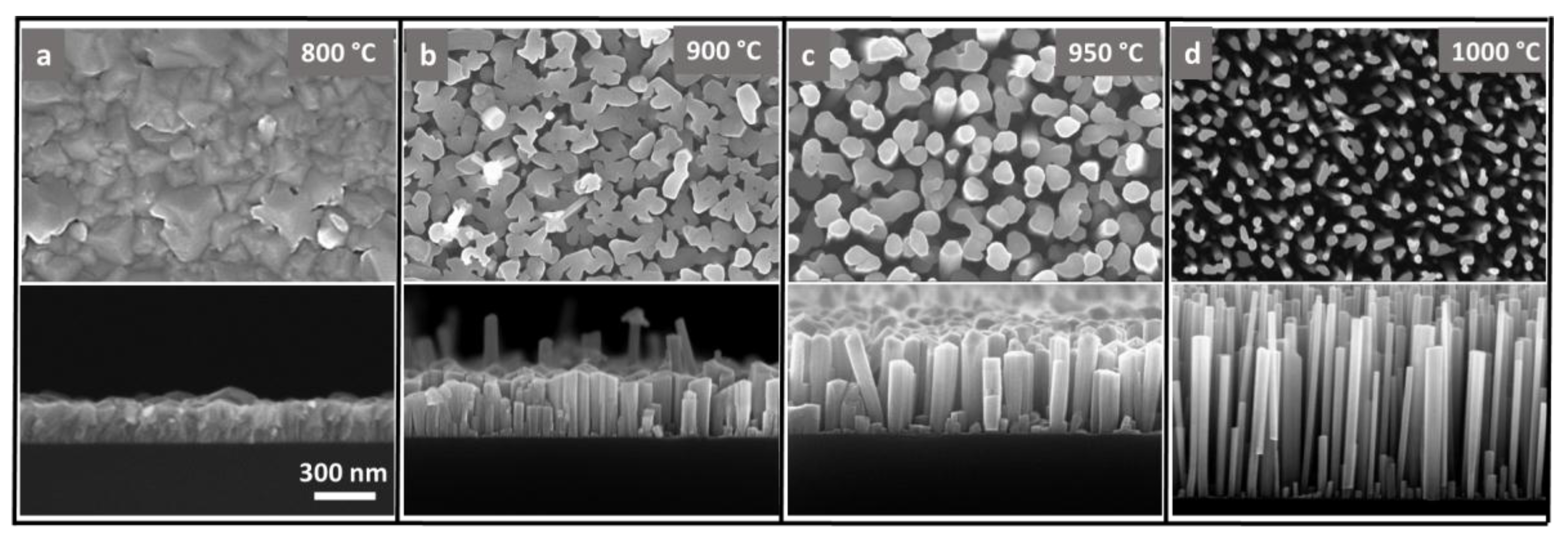
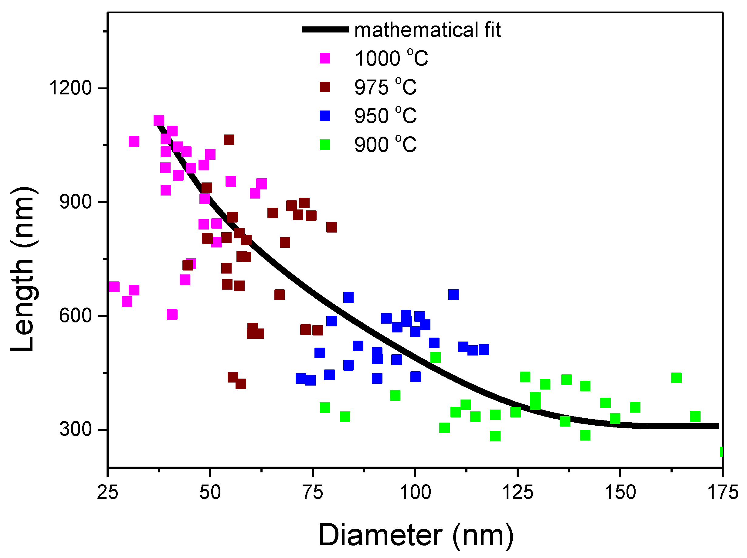
3.1. Growth of GaN NRs Directly onto Si Substrates

Figure 1 shows top- and cross-sectional view SEM images of GaN grown on Si substrate at 800, 900, 950, and 1000 °C for 2 h. As can be seen, the increase in temperature conducts to the formation of NRs with increasing aspect ratio (proportional relationship between NR width and height). At a growth temperature of 800 °C (Figure 1a), a columnar film with a thickness of approximately 300 nm is obtained. At higher temperatures, discrete NRs start to develop, initially with low aspect ratio and nearly coalesced, as can be observed in the 900 °C sample (Figure 1b). At 950 °C (Figure 1c), the NRs outline becomes better defined from the top view, with less coalescence taking place. This process is further enhanced at 1000 °C (Figure 1d), when well-separated NRs are formed even during the initial stages of growth. No exfoliation is visible for the film grown at 800 °C, and in all the samples, a clear interface with good adhesion of the NRs to the substrate is observed.
Figure 2 shows the temperature dependence upon the dimensional distribution (length vs. diameter) of the GaN NRs. The data was obtained from measurements done on the cross-sectional SEM images of the NRs. The sample grown at the lowest temperature, 900 °C, presents the widest diameter spread of more than 100 nm (with a range in between 75 and 175 nm). The length spread is also large—from 240 to 490 nm. The average diameter and length are 128 and 355 nm, respectively. At higher growth temperature, 950 °C, both dimensional distributions get narrower, but particularly the diameter, ranging from 70 to 115 nm, with an average of 95 nm. A small variation is also observed in length, from 450 to 650 nm, with a pronounced maximum at around 528 nm. This trend of decreasing diameters and narrower diameter spread gets more pronounced at higher temperatures. The samples obtained at 975 °C and 1000 °C exhibit similar characteristics: very narrow diameters, of less than 70 nm and a size distribution of around 35 nm. The diameter decrease is correlated with the increase in length so that the NRs measure around double in length when compared to the samples grown at temperatures lower than 950 °C, but also with larger variations.
From the fitted curve in Figure 2, it becomes apparently that the NRs grow with an approximately inverse relation in between length and width with growth temperature. This complies with the kinetic models of Johansson et al. [32,33], where there is a linear dependence of the NR length (L) on the inverse diameter (1/d):
L = C1 (1 + C2/d),
where C1 and C2 are sample specific constants. The value C1 is related to the thickness of a film (280 nm from our previous experiments). The value of C2 is related to diffusion-induced growth and is two times the diffusion length. By fitting this formula to the experimental data, we obtain the average diffusion length, which decreases with the decrease in growth temperature: 57 nm, 54 nm, 41 nm, and 18 nm respectively, for 1000 °C, 975 °C, 950 °C, and 900 °C, respectively. In the case of a film the diameter tends to infinity and the effective redistribution of average diffusion length is approached to 0 (negligible). The diffusion length increases with temperature and adatoms can consequently reach the peak of the NRs. The result is that vertical growth rate becomes larger than the axial growth rate, which favors NR formation. Consequently, the aspect ratio of the NRs increases with the increase of the diffusion length. Also, since we still obtain a high density of NR, the residence time of the adatoms at 1000 °C is large enough so that the majority of adatoms are incorporated in the growth and do not desorb.

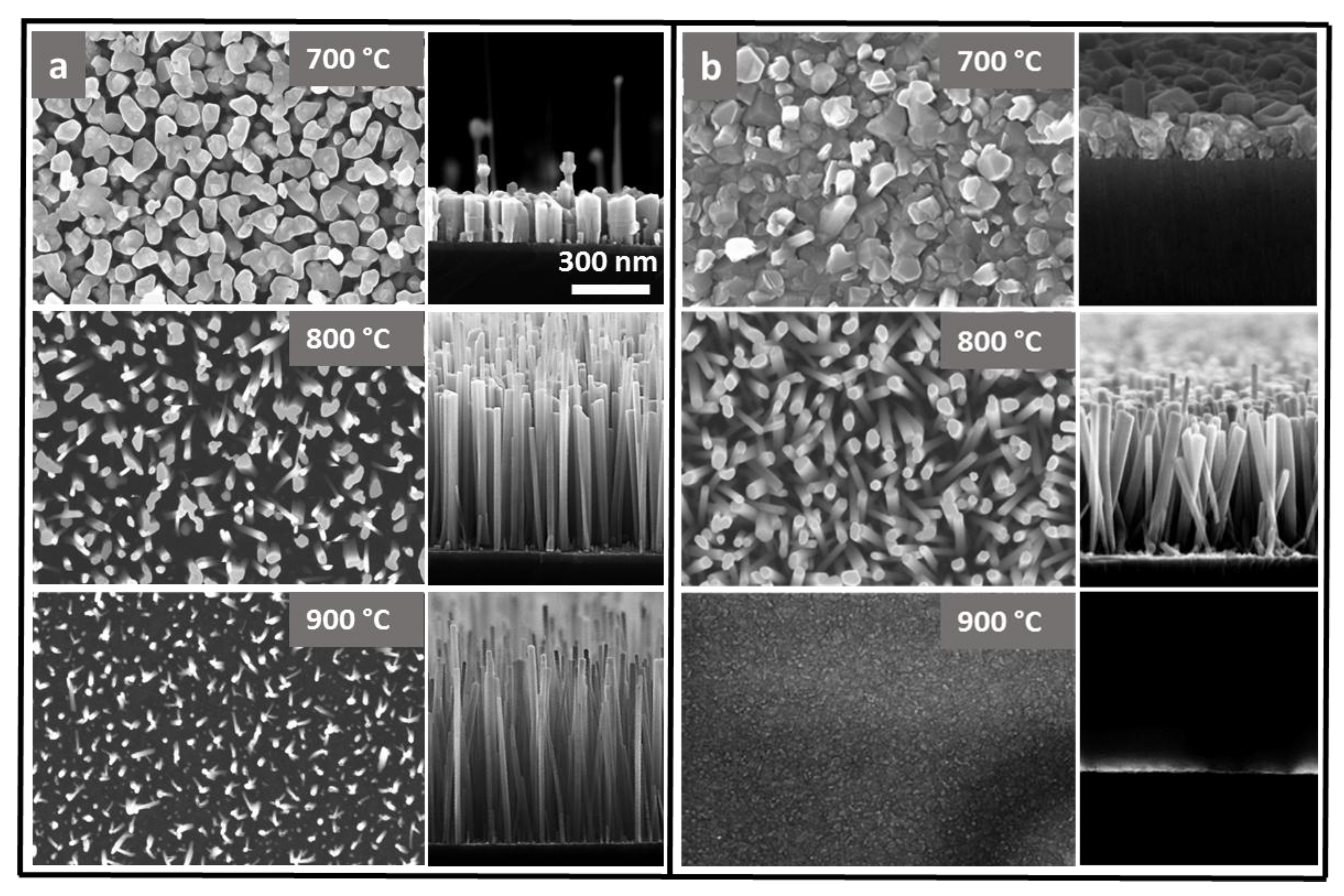
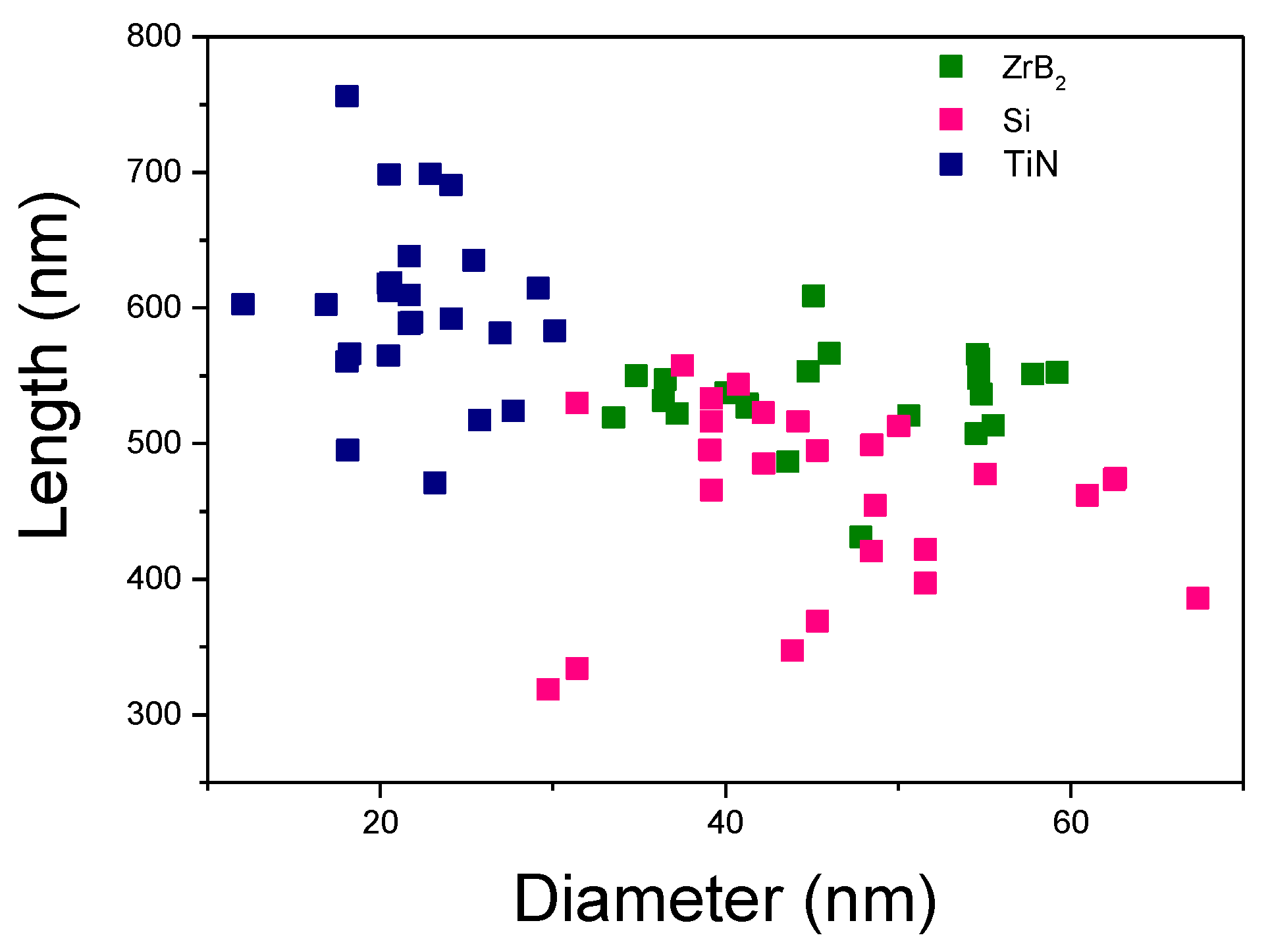
3.2. Growth of GaN NRs on TiN and ZrB2 Conductive Layers

Figure 3 shows comparatively cross-sectional and top views SEM images of GaN NRs grown on (a) TiN/Si and (b) ZrB2/Si templates at different temperatures. As can be seen for the sample grown at 700 °C, NRs were formed on the TiN template but with high non-uniformity in terms of sizes and shapes. At 800 °C, well-separated NRs with small diameter in the range of 40 nm were obtained. The NRs grow perpendicular on the template and have a higher length homogeneity than the NRs grown at lower temperature. When increasing the growth temperature to 900 °C, well-separated and highly homogenous NRs with very narrow diameters of approximately 20 nm are obtained.
The corresponding growth on ZrB2 at 700 °C, resulted in a columnar thin film with column diameters of approximately 150 nm. At 800 °C, the growth results in separated NRs that are tilted with respect to template’s surface normal. There is also a tapering on the top of the rods, which have a smaller diameter at the base in comparison with the top. At 900 °C, no NRs were formed, resulting from the temperature being too high for growth on the template so that the process is dominated by desorption, similar to the TiN template at 950 °C (not shown).
Figure 4 displays the statistical dependence of the dimensional distribution (length and diameter) of the GaN NRs for various templates/substrates. The data was obtained by measuring the NRs visible in the high magnification cross-sectional SEM image. The samples grown in optimized conditions at 800 °C on ZrB2/Si and 900 °C on TiN/Si are presented in comparison with the GaN NRs grown at 1000 °C for one hour on bare Si.
As can be seen, the NRs grown on Si show the widest diameter distribution and smallest length. On ZrB2/Si, the NR diameter distribution range is getting narrower, of only 25 nm, with an average situated at around 45 nm. Correlated with the diameter reduction is the increase in length, the NRs exhibiting a uniform length, of around 550 nm. On TiN/Si, the NR diameter decreases even more, to an average of only 20 nm, confined in a range of only 15 nm. On the other hand, the length variation is larger in this case (of approximately 200 nm, with lengths comprised in between 500 and 700 nm), if compared with the previously discussed case, and the average length is also larger, of around 600 nm, due to the increase in aspect ratio correlated with the decreased diameter. Diameters and size distribution can be tailored by increasing temperatures on Si. On the other hand, if is necessary to achieve very narrow diameters and a better size uniformity, growth on a different material can be employed with better results, for example TiN/Si, in this case.

3.3. Growth of GaN NRs on Metal and SiC Templates/Substrates

Figure 5 shows GaN NRs grown on different templates/substrates. NRs grew on metallic Ti (Figure 5a) only on specific domains of certain orientations of the polycrystalline Ti. They grew tilted with respect to substrate’s surface normal and have an average diameter of approximately 100 nm. In a previous study [34], the growth of GaN NRs is reported on the whole surface of a polycrystalline Ti foil, unaffected by the differently oriented domains. A tilted growth is also observed in this case, and is attributed to the reaction between Ti and Ga, which conducts to the formation of a rough interface. The NRs are uniform both in height and diameter. On the Mo metallic substrate (Figure 5b), NRs do not grow as uniform as in the previous case. Although the tendency is to form NRs with a similar diameter as the previous sample, the sample is characterized by NRs with irregular shapes and sizes, which resulted from the pronounced coalescence. Previous reports of GaN NRs grown on Mo films attribute the tilted growth and coalescence to the rough metal surface underneath [13,14]. On SiC (Figure 5c) the resulting growth is comparable to growth on Si. The growth temperature is the same, 1000 °C, and have a similar aspect: straight NRs with narrow diameters of less than 70 nm. TiN/SiC templates were not used since the quality of the TiN layer would be affected by the larger lattice mismatch and different crystal structure of SiC in comparison to Si. On ZrB2/SiC (Figure 5d), the NRs were grown at the same temperature as on ZrB2/Si, 800 °C. The growth is similar to ZrB2/Si, where tilted NRs are obtained, but in this case, the diameters are almost double, with an average of 80 nm.
MSE is a versatile technique that can be employed for growing nanostructures, which can be used in different applications based on the substrate that they are grown onto. The NRs grown on metallic seed layers, like Ti and Mo, can be used as electrodes because of their excellent optical and electronic properties when integrated in optoelectronic devices. On the other hand, the serious problem of device performance degradation owing to the heat generated during operation can be solved by using SiC substrates. The use of a ZrB2/SiC template makes it possible to combine the excellent heat dissipation feature offered by the SiC with the high electrical conductivity of ZrB2.

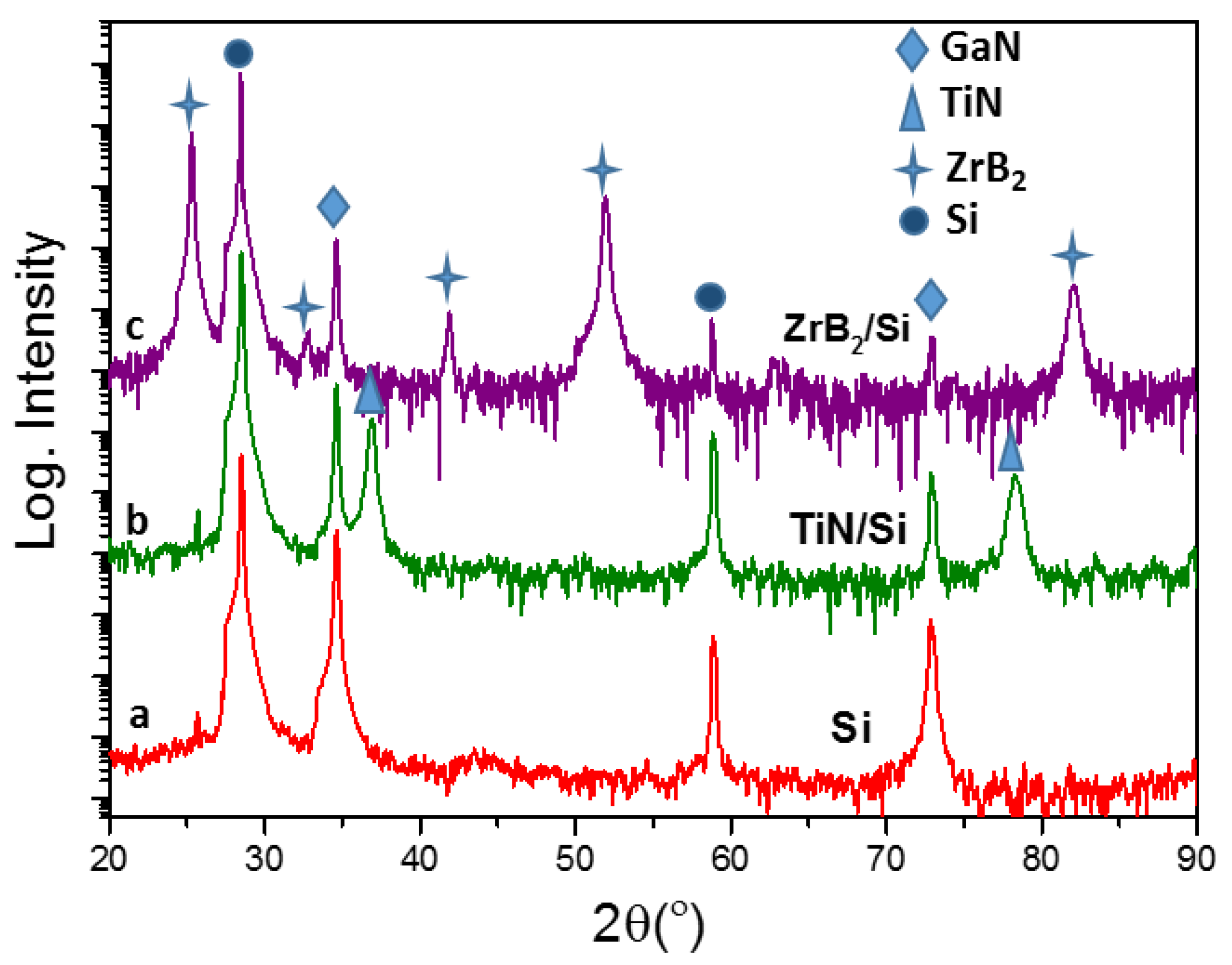
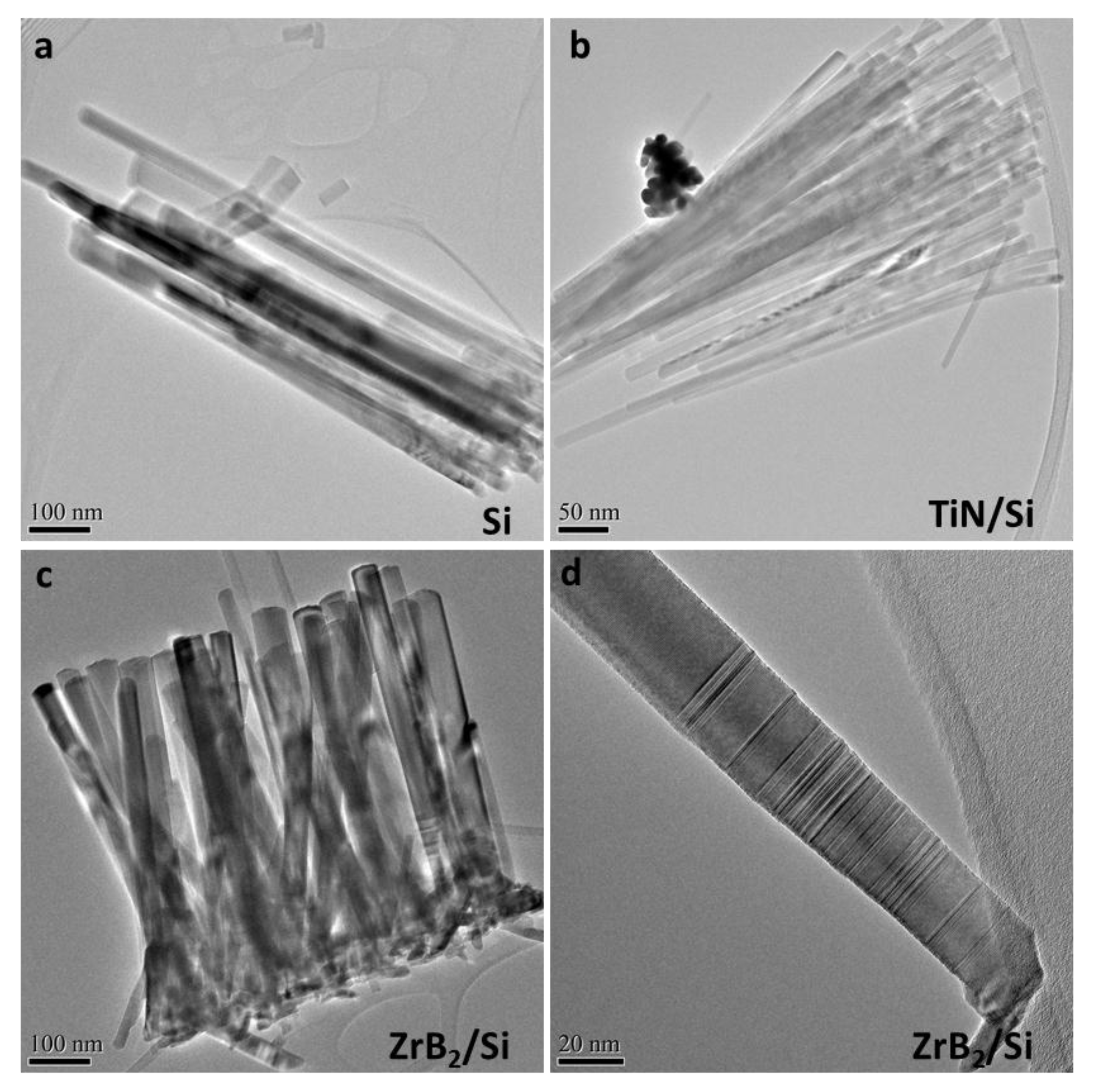
3.4. Structural Characterizations

Semi-logarithmic plotted XRD θ/2θ scans of the GaN NRs grown on different template/substrates are shown in Figure 6. When depositing GaN NRs on bare Si (Figure 6a), except for the strong Si 111 and 222 peaks located at 28.6° and 58.8° and the GaN 0002 and 0004 peaks located at 34.6° and 72.9°, no other distinct peak is found over the long range. The diffractogram looks similar for the sample grown on TiN/Si templates (Figure 6b), except of the two new peaks associated with TiN 111 (36.7°) and TiN 222 (78°) that emerge. On the other hand, the diffraction pattern of the sample grown on ZrB2/Si is more complicated (Figure 6c). The ZrB2 film shows a preferential growth along c-axis, evidenced by the intense ZrB2 0001, 0002, and 0003 peaks, located at 25.3°, 51.8°, and 82°, respectively. Two weak peaks, located at 32.7° and 41.8° and corresponding to 10 1 ¯ 0 and 10 1 ¯ 1 reflections of ZrB2, respectively, can be observed, indicating minor inclusion of other oriented grains as reported in our previous study [30,31]. In addition, only GaN 0002 and 0004 reflections are present in the diffraction patterns, indicating that wurtzite GaN NRs were preferentially grown along 0001 direction in all three samples. The full-width at half-maximum (FWHM) of GaN 0002 reflections is similar in the 3 samples, of around 0.7° indicating similar crystal quality.
To further study the epitaxial relationship between GaN NRs and templates, XRD pole figure measurement was employed. Figure 7 displays the pole figures of (a, b) 10 1 ¯ 1 GaN, (c) 220 TiN, (d) 10 1 ¯ 1 ZrB2, and (e, f) 220 Si reflections. In Figure 7a,b, the six reflections located at psi (Ψ) ~ 62°, corresponding to the angle between 0001 and 10 1 ¯ 1 planes, are attributed to the six-fold symmetry of hexagonal GaN showing that the NRs were grown epitaxial on the templates, with an epitaxial relationship GaN [0001]//Si [111] and GaN [11 2 ¯ 0]//Si [1 1 ¯ 0]. In the 220 TiN and 220 Si pole figures, three sharp reflections distributed with a 120° phi angle, ϕ, spacing presented at Ψ ~ 35° are shown in both pole figures, indicating an epitaxial growth of TiN layer on the Si substrate. The out-of-plane epitaxial relationship is GaN [0001]//TiN [111]//Si [111] and in-plane GaN [11 2 ¯ 0]//TiN [1 1 ¯ 0]//Si [1 1 ¯ 0]. The intensity of the six reflections becomes more diffuse on the ZrB2/Si template on the other hand, see Figure 7b. The elongation along the ϕ angle is attributed to a broad in-plane misorientation, meaning that the NRs exhibits a small-angle twist with respect to each other. The elongation along Ψ angle is due to the tilted growth of the NRs in respect to template’s surface normal, as it can be observed also from the SEM images. The ZrB2 pole figure shown in Figure 7d displays 12 peaks located at Ψ ~ 50°, indicating that the ZrB2 layer was grown as two domains with a 30° in-plane orientation difference. The ZrB2 reflections are not as sharp as the reflections in the TiN pole figure, see Figure 7c, which may result in a poor epitaxial growth of GaN NRs. This is due to a reaction between the Si substrate and ZrB2 film resulting in an amorphous substrate-film interface which affects the quality of the ZrB2 film [30]. The out-of-plane epitaxial relationship is GaN [0001]//ZrB2 [0001]//Si [111] and GaN [11 2 ¯ 0]//ZrB2 [11 2 ¯ 0]//Si [1 1 ¯ 0 ] for the preferential orientation and GaN [11 2 ¯ 0]//ZrB2 [11 2 ¯ 0]//Si [210] for the minority orientation. However, all the grown samples exhibit high crystalline quality according to XRD θ/2θ scans, which show sharp peaks with very narrow linewidths in all samples.
Figure 8 shows an overview TEM image of the free standing GaN NRs that were grown on the different substrates/templates at high temperatures. For NRs grown on Si (Figure 8a), except for a small number of stacking faults (SFs) that develop in the beginning of the growth in some of the NRs (the first 50–100 nm), no additional structural defects were observed. The NRs have an average length of 900 nm and diameters of 30–40 nm. NRs grown on TiN/Si (Figure 8b) resulted in small diameter NRs in the range of 10–15 nm, with an average length of 500 nm and possessing high crystal quality with no obvious structural defects, including SFs. On ZrB2/Si (Figure 8c), on the other hand, the NRs contain a high number of SFs that develop in the beginning of the growth and are present only in the bottom part of the NRs (the first 100–150 nm of the total of 600 nm NRs’ length) as it can be observed in the high-resolution TEM image presented in Figure 8d. Also, the NRs do not have a uniform diameter, a gradually increase with increasing NRs length being visible. The broadening of the NRs in this case can be related with the high number of SFs present. The surface stress induced by the crystal quality, where the ZrB2 film consists of epitaxial columns approximately 20 by 20 nm wide in the x-y direction and 400 nm in the z direction, [30] induces SF formation. With each occurrence of a twin boundary, a step is added in radial direction (Figure 8d). This mechanism is reported in the literatures in the case of III-V and III-nitride NRs grown by vapor-liquid-solid (VLS) method [35,36].

3.5. Optical Properties

The comparative CL spectra for the temperature series grown on Si is presented in Figure 9a. The spectra reveal that the GaN NRs grown on Si at 1000 °C exhibit the strongest bandedge emission, which is centered at around 362 nm. An additionally broad yellow band emission, centered at approximately 560 nm, can also be observed, which is thought to originate from the impurities incorporated during growth [24]. For lower growth temperatures, the NRs possess weak luminescence, which is dominated by the yellow band emission. The improvement of optical and electrical properties for higher growth temperatures was also observed in MOCVD grown NRs. In this case, the measurements on GaN NRs grown at different temperatures showed faster carrier relaxation through the states responsible for defect-related band for lower in comparison to higher growth temperature, attributed to more impurity sites present at lower growth temperature [37,38]. The emission spectra of the samples grown on different substrates/templates are presented in Figure 9b. The luminescence of the samples changes when growing on other templates. On ZrB2/Si, although the sample was grown at a lower temperature of 800 °C, the bandedge emission is still strong, but is comparable in relative intensity with the yellow band emission. On the other hand, the sample grown on TiN/Si at 900 °C has better quality, preserving the strong bandedge emission, but with a barely measurable yellow band. The good optical properties of the sample grown on TiN/Si can be correlated with improved crystal quality observed in the TEM analysis, which can be due to the very narrow diameter of the NRs, making it easier for both line and point defects to be depleted to the NR surfaces.

4. Conclusions

Initially, we report on a temperature series of GaN NRs grown on Si substrates. Lower temperatures result in continuous GaN thin films, while NRs with a low aspect ratio start to form at 900 °C. With increasing growth temperature (up to 1000 °C), the NR’s diameter is reduced and consequently attain higher aspect ratios. By curve-fitting the experimental results, a trend of decreasing diffusion length with increased temperature was observed in agreement with established models.
GaN NRs were also grown on two templates: TiN/Si and ZrB2/Si. TiN layer enables a larger temperature growth window (of more than 200 °C), NRs being obtained at growth temperatures from 700 to 900 °C, in comparison with ZrB2 (less than 100 °C), where NRs grow only at growth temperatures higher than 800 and lower than 900 °C. The aspect ratio of the NRs again increases with temperature on both templates, and a narrower diameter distribution is obtained with increasing growth temperatures. Epitaxial NRs were obtained on both templates, with a higher degree of preferred orientation on TiN. Also, due to the roughness of the ZrB2 layer, the NRs grow tilted, and a tapering effect can also be observed. The GaN NRs grown on ZrB2/Si present a high number of SFs, while the very narrow NRs obtained on TiN/Si show almost crystal perfection, with no structural defects observable by TEM. Our MSE-grown GaN NRs possess strong bandedge emission at high growth temperature on Si and almost no yellow band emission on TiN/Si.
This paper emphasizes the versatility of MSE by proving the growth of GaN NRs on a range of different templates and substrates, each offering alternatives for simpler and more affordable processing in device technology on an industrial scale.

Acknowledgments

This work was supported by the Swedish Research Council (VR) under grants Nos.621-2012-4420, 621-2013-5360, and 2016-04412 and the Swedish Governmental Agency for Innovation Systems (VINNOVA) under the VINNMER international qualification program. The authors further acknowledge the Swedish Foundation for Strategic Research (SSF) through the Research Infrastructure Fellow Program no. RIF 14-0074 and the Knut and Alice Wallenberg Foundation for support from the electron microscopy laboratory in Linköping. The Swedish Government Strategic Research Area in Materials Science on Functional Materials at Linköping University (Faculty Grant SFO-Mat-LiU 2009-00971) is finally acknowledged for financial support.

Author Contributions

E.A.S., M.J., L.H., J.B., and C.-L.H. conceived and designed the experiments; E.A.S., M.J., and C.-L.H. performed the growth of GaN; L.T. and H.H. grew the ZrB2 films and characterized their fundamental properties; J.P and E.A.S. performed TEM and analyzed the data together with P.O. Å.P., L.H., and C.L.-H.; E.A.S., H.H., J.B., and C.-L.H. analyzed XRD data; E.A.S. wrote the manuscript with revision by J.P., H.H., P.O. Å.P., L.H., J.B., L.T., and C.-L.H. All authors agreed on the final version of the manuscript.

Conflicts of Interest

The authors declare no conflicts of interest.

References

  1. Amano, H. Development of GaN-based blue LEDs and metalorganic vapor phase epitaxy of GaN and related materials. Prog. Cryst. Growth Charact. Mater. 2016, 62, 126–135. [Google Scholar] [CrossRef]
  2. Fujita, S. Wide-bandgap semiconductor materials: For their full bloom. Jpn. J. Appl. Phys. 2015, 54, 030101. [Google Scholar] [CrossRef]
  3. Viswanath, A.K. GaN nanostructure-based light emitting diodes and semiconductor lasers. J. Nanosci. Nanotechno. 2014, 14, 1947–1982. [Google Scholar] [CrossRef]
  4. Zhu, D.; Wallis, D.J.; Humphreys, C.J. Prospects of III-nitride optoelectronics grown on Si. Rep. Prog. Phys. 2013, 76, 106501. [Google Scholar] [CrossRef] [PubMed]
  5. Kukushkin, S.A.; Osipov, A.V.; Bessolov, V.N.; Medvedev, B.K.; Nevolin, V.K.; Tcarik, K.A. Substrates for epitaxy of gallium nitride: New materials and techniques. Rev. Adv. Mater. Sci. 2008, 17, 1–32. [Google Scholar]
  6. Gurnett, K.; Adams, T. Native substrates for GaN: the plot thickens. III-Vs Rev. 2006, 19, 39–41. [Google Scholar] [CrossRef]
  7. Li, G.; Wang, W.; Yang, W.; Lin, Y.; Wang, H.; Lin, Z.; Zhou, S. GaN-based light-emitting diodes on various substrates: A critical review. Rep. Prog. Phys. 2016, 79, 056501. [Google Scholar] [CrossRef] [PubMed]
  8. Liu, R.; Ponce, F.A.; Dadgar, A.; Krost, A. Atomic arrangement at the AlN/Si(111) interface. Appl. Phys. Lett. 2003, 83, 860–862. [Google Scholar] [CrossRef]
  9. Kamiyama, S.; Takanami, S.; Tomida, Y.; Iida, K.; Kawashima, T.; Fukui, S.; Iwaya, M.; Kinoshita, H.; Matsuda, T.; Yasuda, T.; et al. Violet and UV light-emitting diodes grown on ZrB2 substrate. Phys. Stat. Sol. (a) 2003, 200, 67–70. [Google Scholar] [CrossRef]
  10. Luther, B.P.; Mohney, S.E.; Jackson, T.N. Titanium and titanium nitride contacts to n-type gallium nitride. Semicond. Sci. Technol. 1998, 13, 1322–1327. [Google Scholar] [CrossRef]
  11. Piper, J. Galvanomagnetic effects in single-crystal ZrB2. Phys. Chem. Solids. 1966, 27, 1907–1915. [Google Scholar] [CrossRef]
  12. Johansson, B.O.; Sundgren, J.-E.; Greene, J.E. Growth and properties of single crystal TiN films deposited by reactive magnetron sputtering. J. Vac. Sci. Technol. A: Vac. Surf. Films 1985, 3, 303–307. [Google Scholar] [CrossRef]
  13. Sarwar, G.; Carnevale, S.D.; Yang, F.; Kent, T.F.; Jamison, J.J.; McComb, D.W.; Myers, R.C. Semiconductor nanowire light-emitting diodes grown on metal: A direction toward large-scale fabrication of nanowire devices. Small 2015, 11, 5402–5408. [Google Scholar] [CrossRef] [PubMed]
  14. Zhao, C.; Ng, T.K.; Wei, N.; Prabaswara, A.; Alias, M.S.; Janjua, B.; Shen, C.; Ooi, B.S. Facile formation of high-quality InGaN/GaN quantum-disks-in- nanowires on bulk-metal substrates for high-power light-emitters. Nano Lett. 2016, 16, 1056–1063. [Google Scholar] [CrossRef] [PubMed]
  15. Nguyen, H.P.T.; Wang, Q.; Mi, Z. Phosphor-free InGaN/GaN dot-in-a-wire white light-emitting diodes on copper substrates. J. Electron. Mater. 2014, 43, 868–872. [Google Scholar] [CrossRef]
  16. Mandl, M.; Wang, X.; Schimpke, T.; Kölper, C.; Binder, M.; Ledig, J.; Waag, A.; Kong, X.; Trampert, A.; Bertram, F.; et al. Group III nitride core–shell nano- and microrods for optoelectronic applications. Phys. Status Solidi RRL 2013, 7, 800–814. [Google Scholar] [CrossRef]
  17. Kanga, M.S.; Lee, C.-H.; Park, J.B.; Yoo, H.; Yi, G.-C. Gallium nitride nanostructures for light-emitting diode applications. Nano Energy 2012, 1, 391–400. [Google Scholar] [CrossRef]
  18. Johnson, J.C.; Choi, H.-J.; Knutsen, K.P.; Schaller, R.D.; Yang, P.; Saykally, R.J. Single gallium nitride nanowire lasers. Nat. Mater. 2002, 1, 106–110. [Google Scholar] [CrossRef] [PubMed]
  19. Ko, S.-M.; Kim, J.-H.; Ko, Y.-H.; Chang, Y.H.; Kim, Y.-H.; Yoon, J.; Lee, J.Y.; Cho, Y.-H. Growth mechanism of catalyst-free and mask-free heteroepitaxial GaN submicrometer- and micrometer-sized rods under biaxial strain: Variation of surface energy and adatom kinetics. Cryst. Growth Des. 2012, 12, 3838–3844. [Google Scholar] [CrossRef]
  20. Li, E.; Cui, Z.; Fu, N.; Xu, R.; Ma, D. Growth and field emission of single-crystalline GaN nanowire with ropy morphology. Mater. Lett. 2015, 139, 426–428. [Google Scholar] [CrossRef]
  21. Cheng, H.; Li, J.; Wu, D.; Li, Y.; Wang, Z.; Wang, X.; Zheng, X. Effects of precursor-substrate distances on the growth of GaN nanowires. J. Nanomater. 2015, 16, 272–277. [Google Scholar] [CrossRef]
  22. Bertness, K.A.; Roshko, A.; Sanford, N.A.; Barker, J.M.; Davydov, A.V. Spontaneously grown GaN and AlGaN nanowires. J. Cryst. Growth 2006, 287, 522–527. [Google Scholar] [CrossRef]
  23. Ristic, J.; Calleja, E.; Fernandez-Garrido, S.; Cerutti, L.; Trampert, A.; Jahn, U.; Ploog, K.H. On the mechanisms of spontaneous growth of III-nitride nanocolumns by plasma-assisted molecular beam epitaxy. J. Cryst. Growth 2008, 310, 4035–4045. [Google Scholar] [CrossRef] [Green Version]
  24. Xiao, H.-D.; Liu, R.; Liu, J.-Q.; Lin, Z.-J.; Mei, L.-M. Growth process from amorphous GaN to polycrystalline GaN on Si (111) substrates. Vacuum 2009, 83, 1393–1396. [Google Scholar] [CrossRef]
  25. Serban, E.A.; Palisaitis, J.; Yeh, C.-C.; Hsu, H.-C.; Tsai, Y.-L.; Kuo, H.-C.; Junaid, M.; Hultman, L.; Persson, P.O.Å.; Birch, J.; et al. Selective-area growth of single-crystal wurtzite GaN nanorods on SiOx/Si(001) substrates by magnetron sputter epitaxy exhibiting single-mode lasing. Sci. Rep. 2017, submitted. [Google Scholar]
  26. Forsberg, M.; Serban, E.A.; Hsiao, C.-L.; Junaid, M.; Birch, J.; Pozina, G. Near band gap luminescence in hybrid organic-inorganic structures based on sputtered GaN nanorods. Sci. Rep. 2017, 7, 1170–1176. [Google Scholar] [CrossRef] [PubMed]
  27. Forsberg, M.; Serban, A.; Poenaru, I.; Hsiao, C.-L.; Junaid, M.; Birch, J.; Pozina, G. Stacking fault related luminescence in GaN nanorods. Nanotechnology 2015, 26, 355203–355211. [Google Scholar] [CrossRef] [PubMed]
  28. Junaid, M.; Chen, Y.-T.; Palisaitis, J.; Garbrecht, M.; Hsiao, C.-L.; Persson, P.O.Å.; Hultman, L.; Birch, J. Liquid-target reactive magnetron sputter epitaxy of high quality GaN(000 1 ¯ ) nanorods on Si(111). Mater. Sci. Semicond. Process. 2015, 39, 702–710. [Google Scholar] [CrossRef]
  29. Junaid, M.; Hsiao, C.-L.; Palisaitis, J.; Jensen, J.; Persson, P.O.Å.; Hultman, L.; Birch, J. Electronic-grade GaN(0001)/Al2O3(0001) grown by reactive DC-magnetron sputter epitaxy using a liquid Ga target. Appl. Phys. Lett. 2011, 98, 141915–141918. [Google Scholar] [CrossRef]
  30. Tengdelius, L.; Birch, J.; Lu, J.; Hultman, L.; Forsberg, U.; Janzen, E.; Högberg, H. Magnetron sputtering of epitaxial ZrB2 thin films on 4H-SiC(0001) and Si (111). Phys. Status Solidi A 2014, 211, 636–640. [Google Scholar] [CrossRef]
  31. Tengdelius, L.; Greczynski, G.; Chubarov, M.; Lu, J.; Forsberg, U.; Hultman, L.; Janzén, E.; Högberg, H. Stoichiometric, epitaxial ZrB2 thin films with low oxygen-content deposited by magnetron sputtering from a compound target: Effects of deposition temperature and sputtering power. J. Cryst. Growth 2015, 430, 55–62. [Google Scholar] [CrossRef]
  32. Johansson, J.; Svensson, C.P.; Martensson, T.; Samuelson, L.; Seifert, W. Mass transport model for semiconductor nanowire growth. J. Phys. Chem. B 2005, 109, 13567–13571. [Google Scholar] [CrossRef] [PubMed]
  33. Dubrovskii, V.G.; Cirlin, G.E.; Soshnikov, I.P.; Tonkikh, A.A.; Sibirev, N.V.; Samsonenko, Y.B.; Ustinov, V.M. Diffusion-induced growth of GaAs nanowhiskers during molecular beam epitaxy: Theory and experiment. Phys. Rev. B 2005, 71, 205325–205330. [Google Scholar] [CrossRef]
  34. Calabrese, G.; Corfdir, P.; Gao, G.; Pfüller, C.; Trampert, A.; Brandt, O.; Geelhaar, L.; Fernández-Garrido, S. Molecular beam epitaxy of single crystalline GaN nanowires on a flexible Ti foil. Appl. Phys. Lett. 2016, 108, 202101–202104. [Google Scholar] [CrossRef]
  35. Chen, Y.; Burgess, T.; An, X.; Mai, Y.-W.; Tan, H.H.; Zou, J.; Ringer, S.P.; Jagadish, C.; Liao, X. Effect of a high density of stacking faults on the Young’s modulus of GaAs nanowires. Nano Lett. 2016, 16, 1911. [Google Scholar] [CrossRef] [PubMed]
  36. Paiman, S.; Gao, Q.; Tan, H.H.; Jagadish, C.; Zhang, X.; Zou, J. Effects of growth rate on InP nanowires morphology and crystal structure. J. Cryst. Growth 2013, 383, 100–105. [Google Scholar] [CrossRef]
  37. Talin, A.A.; Wang, G.T.; Lai, E.; Anderson, R.J. Correlation of growth temperature, photoluminescence, and resistivity in GaN nanowires. Appl. Phys. Lett. 2008, 92, 093105–093107. [Google Scholar] [CrossRef]
  38. Upadhya, P.C.; Li, Q.; Wang, G.T.; Fischer, A.J.; Taylor, A.J.; Prasankumar, R.P. The influence of defect states on non-equilibrium carrier dynamics in GaN nanowires. Semicond. Sci. Technol. 2010, 25, 024017–024022. [Google Scholar] [CrossRef]
Figure 1. Top-(up) and cross-sectional (bottom) view SEM images of GaN NRs grown on Si at different temperatures: (a) 800 °C, (b) 900 °C, (c) 950 °C, and (d) 1000 °C. The same scale applies to all images.
Energies 10 01322 g001
Figure 2. GaN NR length versus diameter distribution as a function of temperature (2 h growth on Si).
Energies 10 01322 g002
Figure 3. SEM images of GaN NRs grown on (a) TiN/Si and (b) ZrB2/Si templates at different temperatures. The same scale applies to all images.
Energies 10 01322 g003
Figure 4. Length versus diameter distribution of GaN NRs grown at optimized temperatures on different templates (1 h growth).
Energies 10 01322 g004
Figure 5. Tilted-view SEM images of GaN NRs grown on various template/substrates (a) polycrystalline Ti, (b) polycrystalline Mo, (c) SiC, and (d) ZrB2/SiC. The figures have the same scale.
Energies 10 01322 g005
Figure 6. θ/2θ scan XRD patterns of GaN NRs grown on various template/substrates (a) Si, (b) TiN/Si, and (c) ZrB2/Si.
Energies 10 01322 g006
Figure 7. Pole-figure XRD measurements of GaN NRs grown on TiN/Si and ZrB2/Si templates shown in (a, c, e) and (b, d, e), respectively. The corresponding pole figures in these two samples are (a) 10 1 ¯ 1 GaN, (c) 220 TiN, and (e) 220 Si, as well as (b) 10 1 ¯ 1 GaN, (d) 10 1 ¯ 1 ZrB2, and (f) 220 Si, respectively.
Energies 10 01322 g007
Figure 8. TEM images of free-standing GaN NRs grown on: (a) Si at 1000 °C, (b) TiN/Si at 900 °C, and (c, d) ZrB2/Si at 850 °C substrates, respectively.
Energies 10 01322 g008
Figure 9. Room-temperature cathodoluminescence spectra of GaN NRs grown (a) at different temperature on Si and (b) on different templates.
Energies 10 01322 g009

