
An All-Electric-Aircraft Tailored SiC-Based Power Factor Correction Converter with Adaptive DC-Link Regulator


1
Department of Electrical Engineering and IT, DIETI, University of Naples Federico II, 80125 Naples, Italy
2
Power Naples Prototype Laboratory, PNP LAB srl, 80122 Naples, Italy
*
Author to whom correspondence should be addressed.
Energies 2017, 10(8), 1227; https://doi.org/10.3390/en10081227
Submission received: 6 July 2017
/
Revised: 4 August 2017
/
Accepted: 15 August 2017
/
Published: 18 August 2017
Abstract
:In recent years the aerospace industry has made a growing effort to develop a quieter and more environmentally friendly aircraft. In particular, several research activities have been focused on innovative solutions aimed at the design/optimization of an on-board electric system fully compatible with this new approach. A first important step in the evolution towards an All Electric Aircraft (AEA) is the replacement of the hydraulic actuators with fully electric ones. The transition process is not easy to carry out, since weight, size and reliability represent highly critical issues for aircraft applications. In this context, the significant improvements in semiconductor technologies can be exploited as a critical means to overcome the constraints mentioned. Indeed, this work proposes a Silicon Carbide (SiC) based Power Factor Correction (PFC) converter, whose design and control have been tailored in order to properly supply a wide range of on-board Electro-Mechanical Actuators (EMA). In particular, while the adopted circuit topology allows for power factor correction and bi-directional power flow, the SiC technology, thanks to the higher efficiency with respect to other semiconductor-based technologies, leads to a significant reduction in the overall system weight/volume. Furthermore, to meet the strict requirements in terms of dynamic and steady state performance imposed by the application, a novel adaptive regulator is conceived. A reduced-scale laboratory prototype of the SiC-based converter (3 kVA) is realized in order to verify the effectiveness of the proposed design and control approach.
1. Introduction
Nowadays, a relevant aviation trend is the All Electric Aircraft (AEA) concept; an aircraft with a centralized electric power system able to supply all aircraft loads and services. The main role of the electric power system is to convert the mechanical power of the shaft engine into electric one, which can then be employed, by means of on-board distribution and conversion systems, to satisfy various kinds of energy requests: heat/cold generation, mechanical actuation, lighting systems, and so on.
Aviation business has grown considerably in the last years, thus leading to a corresponding growth of the aircraft industry, which can assume a fundamental position in the near future thanks to constantly increasing air transportation demand. At the same time, a progressive electric hybridization of aircrafts has been observed. This evolution is driven by the inner properties of the electric energy, which is regarded as a privileged energetic vector [1,2,3,4,5], able to reduce global weight, operation/maintenance costs and environment polling, thanks to the associated high power density together with zero CO2 emissions. As a consequence, advanced electric architectures are being developed with the aim of optimizing the on-board generation, distribution and storage systems with particular regard to performance, reliability and fault tolerance requirements. Indeed, a progressive electrification has interested most of the automotive sectors in the last years, pushing, above all, the development of high power/energy density storage solutions [6]. Nevertheless, a full AEA implementation would require, in most cases, performance levels of the electric storage systems which are not yet available. For this reason, at this stage, the primary objective is to eliminate both hydraulic and pneumatic systems with their associated equipment, thus improving the aircraft performance, especially with reference to medium-range routes [1]. In particular, this approach allows:
- ▪
- reduction of fuel consumption by 8 to 10%
- ▪
- reduction of takeoff weight by 6 to 7%
- ▪
- reduction of direct maintenance costs by 4 to 6%
- ▪
- reduction of maintenance time by 4 to 5%
- ▪
- reduction of life cycle cost by 4 to 5%
For example, the implementation of some AEA elements on А-380, Boeing-787, and so on, has improved operational and economic performance of these aircraft, leading to a fuel consumption reduction in the 17 to 20% range.
Given the reliability, power density and fault-tolerance requirements, a specific development of the key components of the on board electric power system on which an AEA would be based has to be carried out in order to satisfy the constraints imposed. Indeed, this work is focused on a critical component of the power distribution system; the AC/DC converter connected to the main three-phase grid, operating at 200 V/400 Hz (which are electric parameters typical of the aircraft applications). This converter serves a double purpose:
- ▪
- to feed the primary DC voltage for subsequent DC/DC conversion;
- ▪
- to feed directly the actuation systems operating at high voltage.
The AC/DC conversion is usually carried out by using a two stage AC/DC and DC/DC converter usually implemented by a cascaded connection of a three-phase diode rectifier and chopper converter. Alternatively, it is possible to employ a single stage AC/DC converter called a Power Factor Correction (PFC) converter. This architecture can be obtained by different circuit topologies and by using silicon (Si) or silicon-carbide (SiC) based components. One stage AC/DC conversion can be achieved by using different topologies [7]:
- ▪
- Third harmonic current injection rectifier
- ▪
- Delta switch rectifier
- ▪
- Vienna rectifier
- ▪
- Swiss rectifier
- ▪
- Six switches Current Source Rectifier (CSR)
- ▪
- Six Switches Voltage Source Rectifier (VSR)
Each topology has its own advantages/disadvantages with respect to number of components, efficiency, control complexity, modularity, power quality indexes. In particular, for aircraft application, where the fault tolerance and efficiency attributes are the most critical ones, the more appropriate topology appears to be the Voltage Source Rectifier (VSR) [8,9]. Indeed, the VSR architecture allows the control of the input AC currents with minimum circuit complexity; moreover, its basic configuration can be easily re-arranged in interleaved structures, thus ensuring higher fault-tolerance capabilities.
This paper proposes a PFC SiC-based VSR converter in its standard configuration. The SiC solution guarantees [10,11]:
- ▪
- high efficiency operation: the SiC components exhibit substantial efficiency improvement over the conventional Si based ones;
- ▪
- Electro-Magnetic Interference (EMI) input filter size reduction: the SiC adoption allows to operate at very high switching frequency thus simplifying the design of the input passive filter;
- ▪
- weight and size reduction: SiC devices ability to operate at higher temperature allows to minimize the cooling system size with a subsequent significant bulk reduction.
The SiC hardware solution has been paired with a proper software control solution in order to satisfy the strict performance requirements of the application considered. In particular, a novel DC-Link adaptive regulator has been conceived with the aim to improve both transient and steady state operations. The first part of this work deals with the mathematical model and the control algorithm of the PFC converter. A sizing procedure is then presented for the design/realization of a scaled prototype (3 kVA). Finally, both simulations and experimental tests are shown. The obtained results validate the effectiveness of the proposed PFC solution.
2. Mathematical Model
The proposed topology of Power Factor Correction converter is shown in Figure 1.
This architecture falls in the VSR converter category. For each leg it employs two SiC devices, pulsed in complementary logic. The neatness of this configuration leads to a concise mathematical model:
with the space vectors of the phase grid voltages, of the line currents, of the converter voltages. can be expressed as:
where is the space vector of the fundamental positive sequence, while is the space vector of the residual harmonic sequences. Equation (1) can be conveniently referred to a rotating frame synchronous with :
It should be noted that, by the choice of the reference frame, if the currents components , are constant, then the line currents are sinusoidal and symmetrical, thus absorbing average power only from the phase voltages fundamental positive sequence. The converter voltages , which are the control variables in Equation (3), will be computed by the proposed control strategy.
3. Control Strategy
The control strategy has the aim to keep constant the DC-Link voltage , while absorbing from the grid a set of sinusoidal and symmetrical currents with unitary power factor. The overall control diagram is depicted in Figure 2. The input variables (left side of Figure 2) are the phase to phase voltages, the line currents and DC-Link voltage; the output variable (right side of Figure 2) is the reference space vector converter voltage, which is in turn the input of a space vector modulator block. The proposed algorithm is based on cascaded control: the outer loop regulates , while the inner loop regulates the AC currents.
The outer loop is built around a special proportional-integral (PI) adaptive regulator (check Section 3.1), whose output is the reference grid power , which in turn gives the reference d axis current . Indeed, the DC-Link voltage can be controlled by means of the active power absorbed by the grid:
Equation (4) can be exploited to compute the reference current able to control the DC-Link voltage:
The reference current is instead set to zero with the aim to minimizing the line currents RMS value by achieving a unitary power factor. Since the currents tracking is performed in the fixed frame, the references , are then reported by the transformation:
with the reference of the line currents space vector in the fixed frame and the instantaneous phase angle of . The phase angle is provided by a dq Phase Locked Loop (PLL) [12] which operates on the phase to phase grid voltages.
The reference drives the control inner loop, which is built around a minimum delay deadbeat controller [13], which imposes the tracking of the AC reference space vector current with a delay equal to two sampling intervals:
with the boost inductance, the sampling time interval and the generic sampling time instant.
3.1. The Adaptive PI Regulator
The inner control loop should be able to guarantee reasonable overshoot/undershoot values of in transient condition, while being at the same time highly insensitive to DC-Link voltage ripples linked to load and/or electric grid intrinsic irregularities, such as dissymmetry in the source voltages or low frequencies components in the load power. These requirements are fully met by the proposed novel adaptive PI regulator.
The DC-Link power equation can be written as:
where is the instantaneous power absorbed by the load. The sizing procedure of the proposed PI regulator can be easily conceived once the Equation (8) is properly simplified. In particular, by neglecting the boost inductors instantaneous power, typically a very small ratio of the rated power, and furtherly by considering that the grid power is dependent almost only on the interaction between and , Equation (8) becomes:
Finally, by imposing , it can be easily verified that the Equation (9) can be linearized under the hypothesis :
This equation can be employed in order to size the PI regulator with respect to two different requirements: fast dynamic performance in transient conditions and strong disturbances rejection in steady state conditions. In particular, a satisfying system response, with respect to overshoot and settlement time dynamic properties, can be obtained by imposing that the real and imaginary components of the poles associated to the second order closed loop system are equal. It can be verified that the following relation applies:
with the proportional, integral components of the PI regulator. Therefore, since is linked to as per Equation (11), the adaptive law is formulated once a criterion to adapt is chosen. The proposed novel PI regulator employs two different values for : the transient value and the steady state value . are sized by using the following conditions:
Equation (12) ensures that the PI regulator proportional component output is (i.e., a ratio of the rated power ) when the input error is (i.e., a ratio of the reference DC-Link voltage ). The proposed values for and , relative to transient and steady state conditions, are shown in Table 1.
The chosen values of guarantees that the PI regulator, driven by the steady state components , is able to keep the instantaneous voltage error under in correspondence of slow perturbations, while being highly insensitive to grid/load disturbances. On the other hand, the chosen values of the transient components confer a fast dynamic performance to the PI regulator, which, driven by the components , is able to keep the error around in presence of strong perturbations. The effective PI regulator components are set by means of the following procedure:
- when is greater than the PI regulator components are set to the transient components;
- when is kept under for an assigned time interval Ta, hence defined the PI regulator adaptive time, the following adaptive law is used:i.e., , varies linearly, quadratically between the correspondent boundaries. In order to ensure a soft transition and to avoid stability issues, it is just enough to ensure that Ta is much greater than the settlement time granted to the closed loop system by the PI regulator driven with the transient components.
The proposed adaptive PI regulator has been tested numerically by performing a simulation in Matlab/Simulink™ environment with reference to a system characterized by , and (check next section); the PI regulator adaptive time Ta has been set to 0.5 s, i.e., around 25 times the system settlement time.
Starting from a steady state condition with no load, at 0.5 s a rated load step variation occurs. The load condition is characterized by an assigned disturbance, equivalent to a 10% dissymmetry in the grid voltages. The relative effect is characterized with a harmonic injection at 800 Hz (i.e., two times the grid frequency of the considered electric system, check Section 4) in the load power. Figure 3 shows the behavior of the reference active power ratio , of the relative voltage error and of the proportional component . It can be noted that, in correspondence of the load perturbation at 0.5 s, the PI components are set almost instantaneously to the transient values; indeed the maximum undershoot is kept around 6%; however in the subsequent steady state operation, the reference active power oscillates considerably (±15%), due to the relatively high bandwidth of the PI regulator in this condition. This undesirable oscillation is practically zeroed by the proposed adaptive action which starts at 1 s and terminates at 1.5 s: indeed the reference active power is practically constant in the remaining time interval.
It can be concluded that the proposed adaptive PI regulator shows optimal performance both in steady state and transient condition with no need of a compensation action based on the DC load current measurement [14].
4. LC Filter Sizing Procedure
The proposed sizing procedure refers to a 3 kW PFC converter connected to a 200 V/400 Hz three-phase electric system with a rated DC-Link voltage of 360 V.
First, the optimal values of the boost inductance and of the DC-Link capacitance have to be determined. While should be chosen in order to minimize the line currents Total Harmonic Distortion (THD), the capacitance value should guarantee proper dynamic performance of the converter with respect to the DC-Link voltage undershoots/overshoots in transient conditions. A simple expression of the THD can be obtained if the converter output voltages are considered sinusoidal waveforms with superimposed rectangular alternative waveforms with amplitude and frequency . Under this hypothesis, it can be shown that the following relation is found:
with the rated DC-Link voltage and the line currents rated value. The sizing of the DC-Link capacitor is carried with reference to a load step variation in which the power transferred to the load instantaneously changes from to , with the PFC rated power. In this condition, the converter is able to drive the grid currents with a maximum power derivative given by
where is the grid rated voltage, the converter boost factor and the rated angular frequency. Therefore, the DC-Link equation can be written as:
From (10) the time behavior is easily obtained:
The minimum value of , which quantifies the DC-Link undershoot with respect to the considered worst case condition, is reached at the undershoot time and is given by:
By considering the undershoot much smaller than , the capacitance value that complies with the desired relative DC-Link undershoot voltage can be synthetically expressed as:
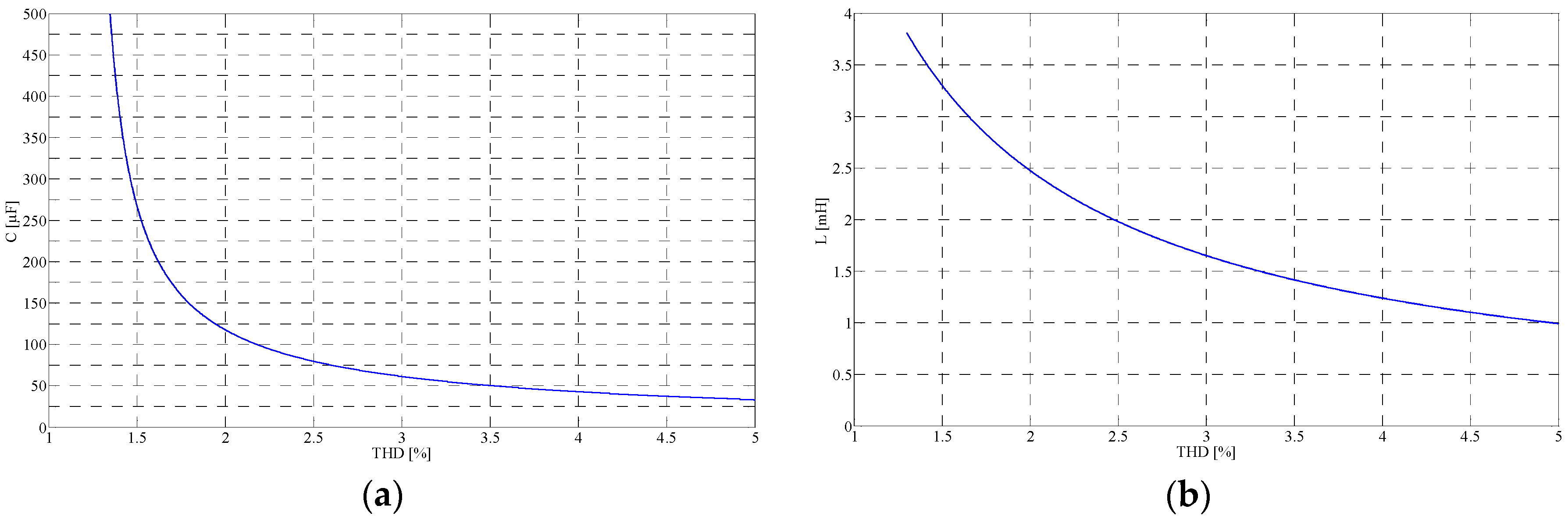
Since depends on the boost inductance as per Equation (15), and depends on the desired THD as per Equation (14), the functions and can be obtained. In particular, Figure 4 shows the values that satisfy an imposed set to for different values of the desired THD in the range .
As it can be noted from Figure 4a, the capacitance value rapidly decreases up to a THD value of about 2%. This consideration leads the optimal choice of the target THD, which has been set to 2.5%. The corresponding filter values are and , respectively.
5. SiC Technology
The intrinsic characteristics of the SiC power devices can be exploited in order to significantly reduce the total weight/volume of the aircraft on board electric power system, thus satisfying critical issues that are typical of the aircraft applications. The SiC Wider Band Gap energy with respect to Si devices allows the SiC semiconductor to operate at higher junction temperature and to sustain a higher breakdown electric field. Therefore, at equal breakdown voltage, SiC devices are characterized by a thinner drift region and higher doping levels, consequently presenting a reduced specific conductive resistance and a lesser sensitivity to the operating temperature with regards to Si devices. The resulting reduced conduction losses, together with the possibility of operating at higher switching frequency, allows to improve the overall system efficiency. Since the power dissipation directly relates to the heat generation, the SiC performance allows to minimize the size of the power devices cooling system. Table 2 compares the main characteristics of the Metal–Oxide–Semiconductor Field-Effect Transistor (MOSFET) SiC based module CCS020M12CM2 by Cree with that of the IGBT Si based module FS25R12W1T4 by Infineon. From the reported data, the overall power dissipations (i.e., switching and conduction losses) of the considered modules at the aforementioned operating conditions are respectively 42 W and 138 W per component. By considering a maximum operating ambient temperature Ta = 25 °C and by taking into account that the junction-case temperature differences in the rated conditions are respectively 29.4 °C and 96.6 °C, the required minimum thermal resistances for the heatsinks are respectively 0.76 °C/W and 0.07 °C/W. This very high ratio (≅10) between the target heatsink thermal resistances leads to a substantial decrease of the size/weight of the cooling system (>1/10). The SiC choice appears therefore the optimal solution in the context of the aircraft applications.
6. Numerical Results
A preliminary numerical analysis has been conducted in order to validate both the control strategy and the sizing procedure. Several simulations have been performed in the Matlab/Simulink™ environment. In particular, the control algorithm has been developed directly in C-language code and implemented in the software by the integrated S-Function resources. This approach allowed the direct transfer of the control code on the Digital Signal Processor (DSP) hardware target device used during the experiments. The system’s main parameters, together with the control quantities, are reported in Table 3.
The whole simulation is performed over a time interval of 2 s. In order to evaluate the system performance under a worst-case scenario, unsymmetrical grid voltages have been considered by injecting a fundamental negative sequence with an amplitude set to 10% the rated one. In the first step, with no load, as soon as the PLL synchronizes, the DC-Link voltage is boosted to its rated value (360 V). At around 0.35 s a load step variation from zero to 3 kW occurs. Finally, at around 1 s, the load changes from 3 kW to zero. The boost action and the load perturbations are clearly highlighted by the grid power P behavior depicted in Figure 5a. From Figure 5b, it can be deduced that the voltage overshoot is lower than 50 V while the relative undershoot is contained under 10% (≅40 V). The unsymmetrical voltages cause a ripple at , which affects both and . In any case, this disturbance is handled with good dynamic performance by the proposed adaptive DC-Link PI regulator. Indeed, the adaptation of the PI constants leads to a substantial decrease of the considered ripples, as can be noted at around 0.6 s, when the regulator adaptive action has been concluded.
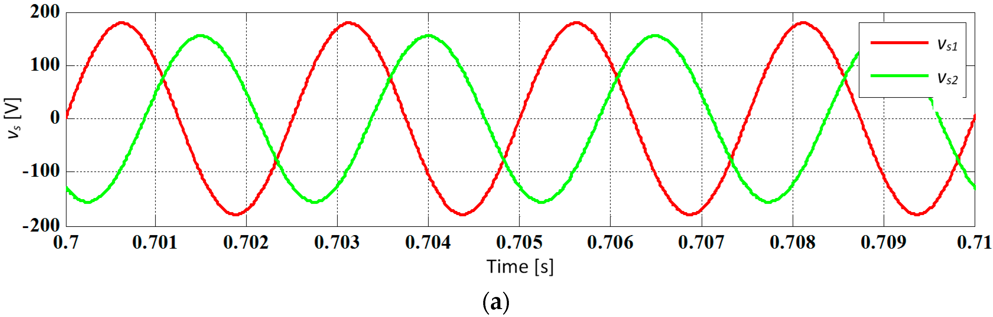
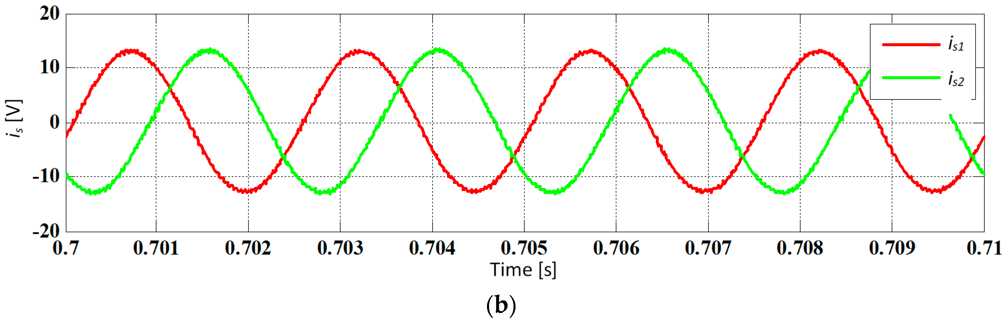
The effectiveness of the DC-Link controller is confirmed in Figure 6, where the behavior of the grid voltages and of the line currents are detailed with reference to a steady state condition at the rated load. Indeed, even under a strong unsymmetrical supply, the line currents are practically sinusoidal and symmetrical, that is, the DC-Link voltage ripple generated by the grid voltages negative sequence is almost totally filtered out by the PI adaptive controller. The analysis carried out confirms that the proposed control is characterized by good dynamic performance at transient conditions and excellent disturbance rejection at steady state operations. Moreover, the THD evaluated is 2.25%, a value very close to the one imposed analytically (2.5%). Both the THD value obtained and the DC-Link voltage undershoot/overshoot therefore highlight the quality of the proposed sizing procedure.
Finally, Figure 7 shows the time behavior of dissipated power Pj (Figure 7a) and maximum junction temperature Tj (Figure 7b) related to the SiC modules. These results have been obtained by implementing a dynamic thermal mode of the electronic devices based on the components datasheet. It should be noted that the expected efficiency of the converter, in rated condition, is around 97.5%.
7. Experimental Results
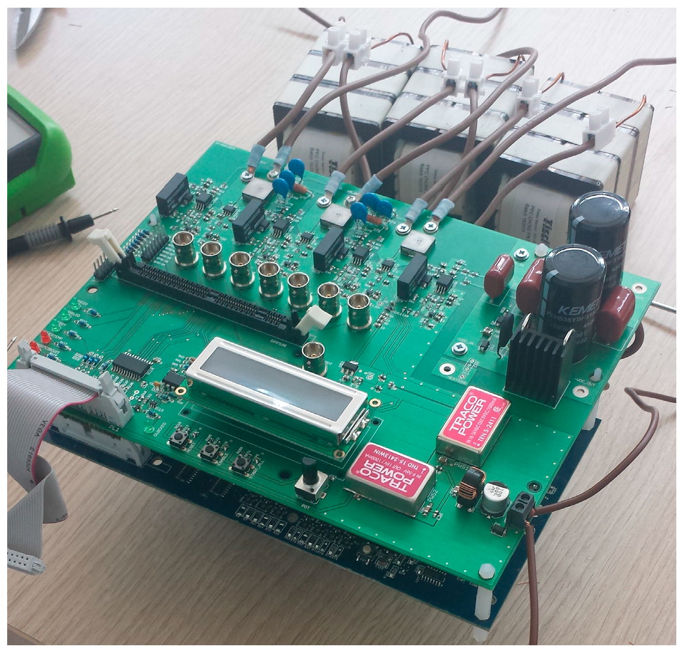
The core of the technological innovation of the proposed conversion system is represented by the replacement of conventional Si based devices with SiC technology. In particular, the prototype has been built around the CCS020M12CM2 1.2 kV/20 A modules by CREE [15], driven by a CREE gate driver [16]. The control algorithm has been implemented on the Digital Signal Processor (DSP) Texas SM320F28335-EP [17]. All the components have been mounted on a custom PCB together with required voltages/currents transducers. Figure 8 shows the realized prototype.
To prove the feasibility of the proposed control strategy, four different tests have been conducted:
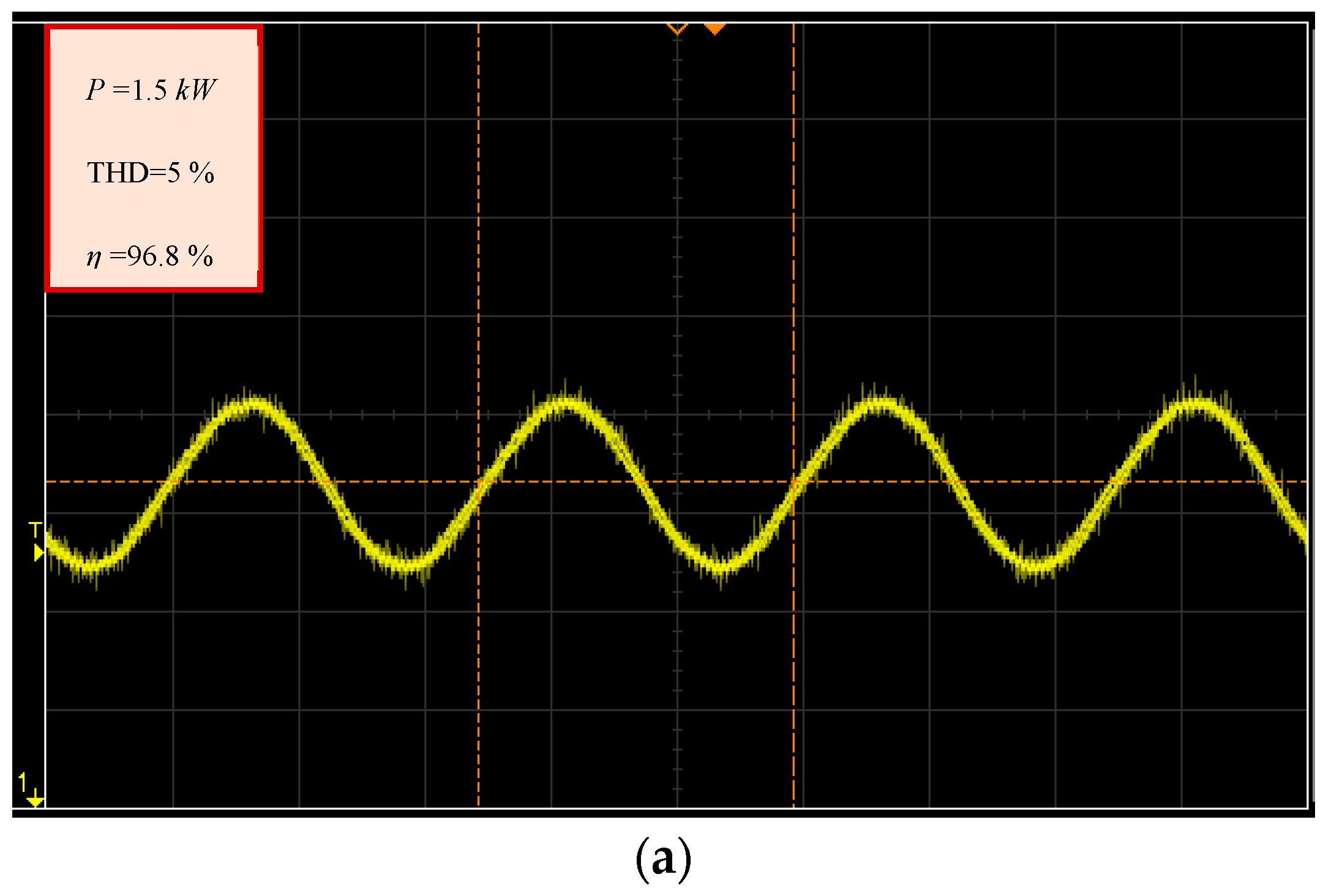
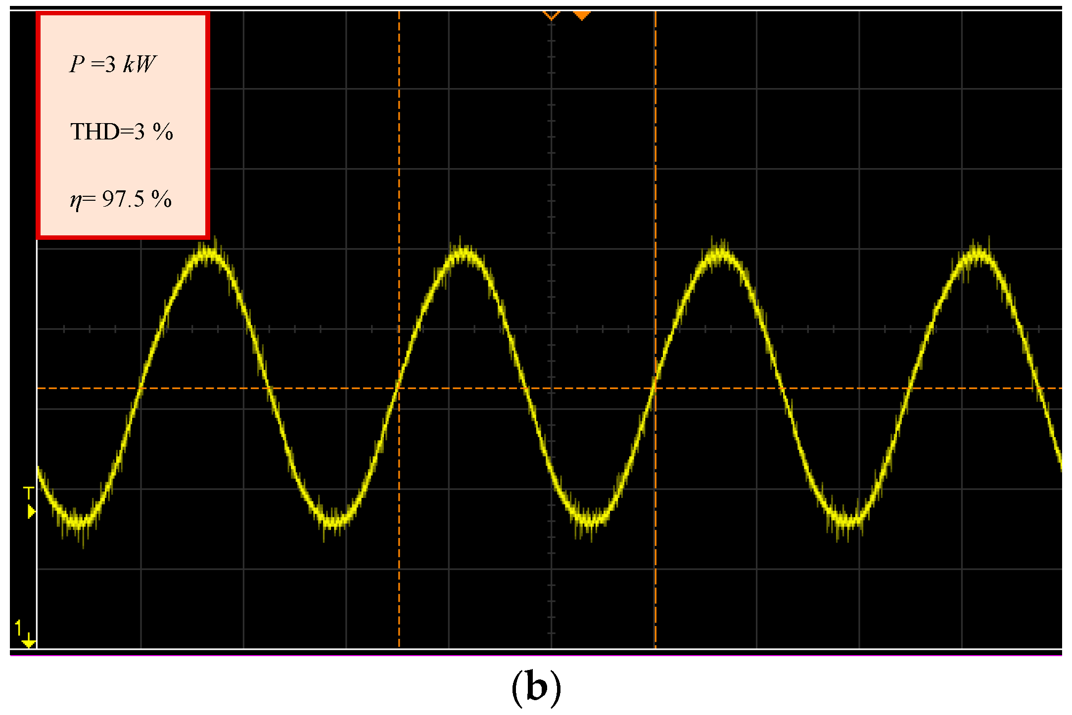
In particular, it can be noted that the undershoots (that occur at around 0.2 s in Figure 9b,c) and the overshoot (that occurs at around 0.2 s in Figure 9d) of the DC-Link voltage are kept under 15%, thus confirming the results of the numerical analysis. The action of the adaptive PI controller also leads to similar results, with the DC-Link voltage ripple decreasing as the adaptive action is executed. Finally, Figure 10 shows the behavior of one line current in steady state condition with P = 1.5 kW (Figure 10a) and P = 3 kW (Figure 10b). The THD factors computed are 5% and 3% respectively, while the overall efficiency is 96.8% and 97.5% respectively. It can be pointed out that the numerical and experimental data are practically coincident with respect to the 3 kW load condition.
8. Conclusions
This work has been focused on the design and control of a SiC-based VSR converter.
The analytical model of the converter has been used to derive analytically the optimal values of the DC-Link capacitance C and boost inductance L with respect to both steady state conditions (low line currents THD) and transient operations (contained DC-Link voltage overshoot/undershoot).
The VSR control strategy has been coupled with a novel adaptive DC-Link PI controller, conceived with the aim of achieving sinusoidal and symmetrical line currents even under strong load/grid disturbances, while keeping the DC-Link voltage close the reference one even under strong load perturbations.
A set of simulations has been performed in order to validate the approach presented. The numerical results confirm the effectiveness of the sizing procedure and highlight the good performance of the proposed adaptive PI regulator.
Furthermore, an experimental campaign has been conducted on a 3 kW SiC-based PFC converter prototype. The experimental results have confirmed the simulated ones obtained under Matlab/Simulink™ environment, showing the capability of the system to take all relevant parameters under control: power factor, line currents THD and DC-Link voltage.
High level efficiency operations have been achieved in spite of the considerable target switching frequency as a result of the SiC technology employed. Indeed, it is worth noting that the total weight of the SiC-based prototype realized (boost inductors excluded) is around 1.1 kg, of which 0.6 kg are related to the heatsink. It should be pointed out that a comparable Si-based converter would require a much larger heatsink, resulting in a total weight exceeding 3 kg.
Acknowledgments
Power Naples Prototype Laboratory PNP LAB SRL Milan, Italy.
Author Contributions
Gianluca Brando implemented the control on the hardware target; Marina Coppola performed the hardware design; Adolfo Dannier conceived the control algorithm; Andrea Del Pizzo written the paper.
Conflicts of Interest
The authors declare no conflict of interest.
List of Symbols
| DC-Link capacitance/Boost inductance | |
| Line currents/Output power/DC-Link voltage/Grid voltages rated values | |
| Mean active power absorbed by the grid | |
| Converter rated power | |
| Instantaneous power absorbed by the load | |
| Proportional, integral components of the adaptive PI regulator | |
| Rated power ratio | |
| Relative DC-Link voltage error | |
| Switching frequency/Sampling time interval | |
| Converter boost factor | |
| Line current/Converter voltage/Phase voltage of the kth phase | |
| Line currents space vector | |
| Line currents space vector components in the synchronous frame | |
| Maximum power time derivative in the worst case condition | |
| Relative DC-Link voltage undershoot | |
| Converter/Phase voltages space vector | |
| Residual harmonics/Fundamental positive sequence of the phase voltages space vector | |
| Converter/Phase voltages space vector components in the synchronous frame | |
| Instantaneous phase angle/Angular frequency of the fundamental positive sequence of |
References
- Levin, A.V.; Musin, S.M.; Khfritonov, S.A.; Kovalev, K.V.; Gerasin, A.A.; Khalyutin, S.P. All-Electric Aircraft. Idea and Technology, 2nd ed.; USATU: Ufa, Russia, 2014; p. 388. [Google Scholar]
- Bertinov, A.I. Aircraft Electrical Generators; Oborongiz: Moscow, Russia, 1959; p. 594. [Google Scholar]
- Kulebakin, V.S.; Morozovsky, V.T.; Sindeev, I.M. Aircraft Power Supply; Oborongiz: Moscow, Russia, 1956; p. 482. [Google Scholar]
- Sindeev, I.M.; Savelov, A.A. Aircraft Electric Power Systems; Transport: Moscow, Russia, 1990; p. 296. [Google Scholar]
- Zontov, V.M.; Kuprin, B.V. Aircraft Electric Power Systems; Transport: Moscow, Russia, 1988; p. 394. [Google Scholar]
- Matthé, R.; Eberle, U.; Pistoia, G. The voltec system: Energy storage and electric propulsion. In Lithium-Ion Batteries: Advances and Applications; Elsevier Science: Oxford, UK, 2013; pp. 151–176. [Google Scholar]
- Kolar, J.W.; Friedli, T. The Essence of Three-Phase PFC Rectifier Systems. In Proceedings of the 2011 IEEE 33rd International Telecommunications Energy Conference (INTELEC), Amsterdam, The Netherlands, 9–13 October 2011. [Google Scholar]
- Zhang, R.; Lee, F.C.; Boroyevich, D. Four-Legged Three-phase PFC Rectifier with Fault Tolerant Capability. In Proceedings of the IEEE 31st Annual Power Electronics Specialists Conference, PESC 00. 2000, Galway, Ireland, 23 June 2000. [Google Scholar]
- Hirachi, K.; Nakaoka, M. Novel PFC converter suitable for engine-driven generator-interactive three-phase power systems. IEE Electr. Power Appl. 1999, 146, 253–260. [Google Scholar] [CrossRef]
- Rabkowski, J.; Peftitsis, D.; Nee, H.P. Silicon Carbide Power Transistors: A New Era in Power Electronics Is Initiated. IEEE Ind. Electr. Mag. 2012, 6, 17–26. [Google Scholar] [CrossRef]
- Levron, Y.; Kim, H.; Erickson, R.W. Design of EMI Filters Having Low Harmonic Distortion in High-Power-Factor Converters. IEEE Trans. Power Electr. 2014, 29, 3403–3413. [Google Scholar] [CrossRef]
- Da Silva, S.A.O.; Coelho, E.A.A. Analysis and Design of a Three-Phase PLL Structure for Utility Connected Systems under Distorted Utility Conditions; CIEP: Sèvres, France, 2004. [Google Scholar]
- Viet, L.H.; Buichner, P.; Muller, V.; Lan, P.N. Deadbeat Current Controller of Front-End Converter with State Observer-Based Predictor; IEEE PEDS: Kuala Lumpur, Malaysia, 2005. [Google Scholar]
- Guzman, R.; de Vicuña, L.G.; Morales, J.; Castilla, M.; Matas, J. Sliding-Mode Control for a Three-Phase Unity Power Factor Rectifier Operating at Fixed Switching Frequency. IEEE Trans. Power Electr. 2016, 31, 758–769. [Google Scholar] [CrossRef]
- CREE CCS020M12CM2 Datasheet. Available online: http://www.wolfspeed.com/media/downloads/187/CCS020M12CM2.pdf (accessed on 3 May 2016).
- CREE CGD15FB45P Datasheet. Available online: http://www.wolfspeed.com/downloads/dl/file/id/836/product/189/cgd15fb45p1.pdf (accessed on 4 July 2016).
- Texas SM320F28335-EP Digital Signal Controller (DSC) Datasheet. Available online: http://www.ti.com/lit/ds/symlink/sm320f28335-ep.pdf (accessed on 1 March 2016).
Figure 1.
Proposed Power Factor Correction (PFC) converter.
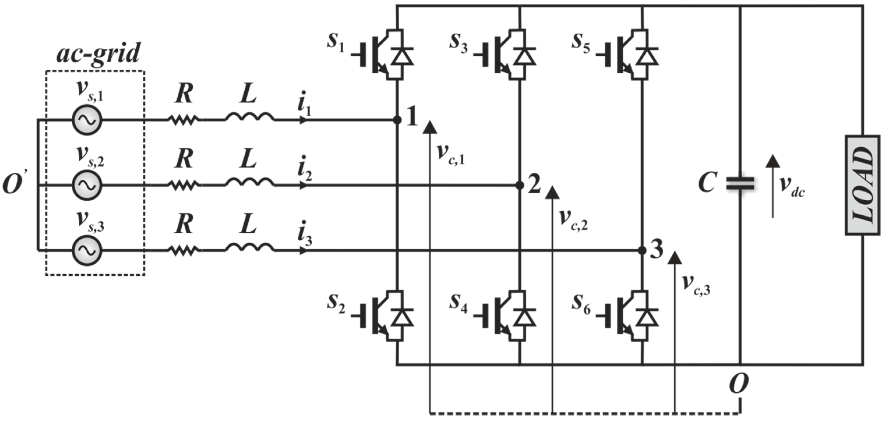
Figure 2.
Control diagram.
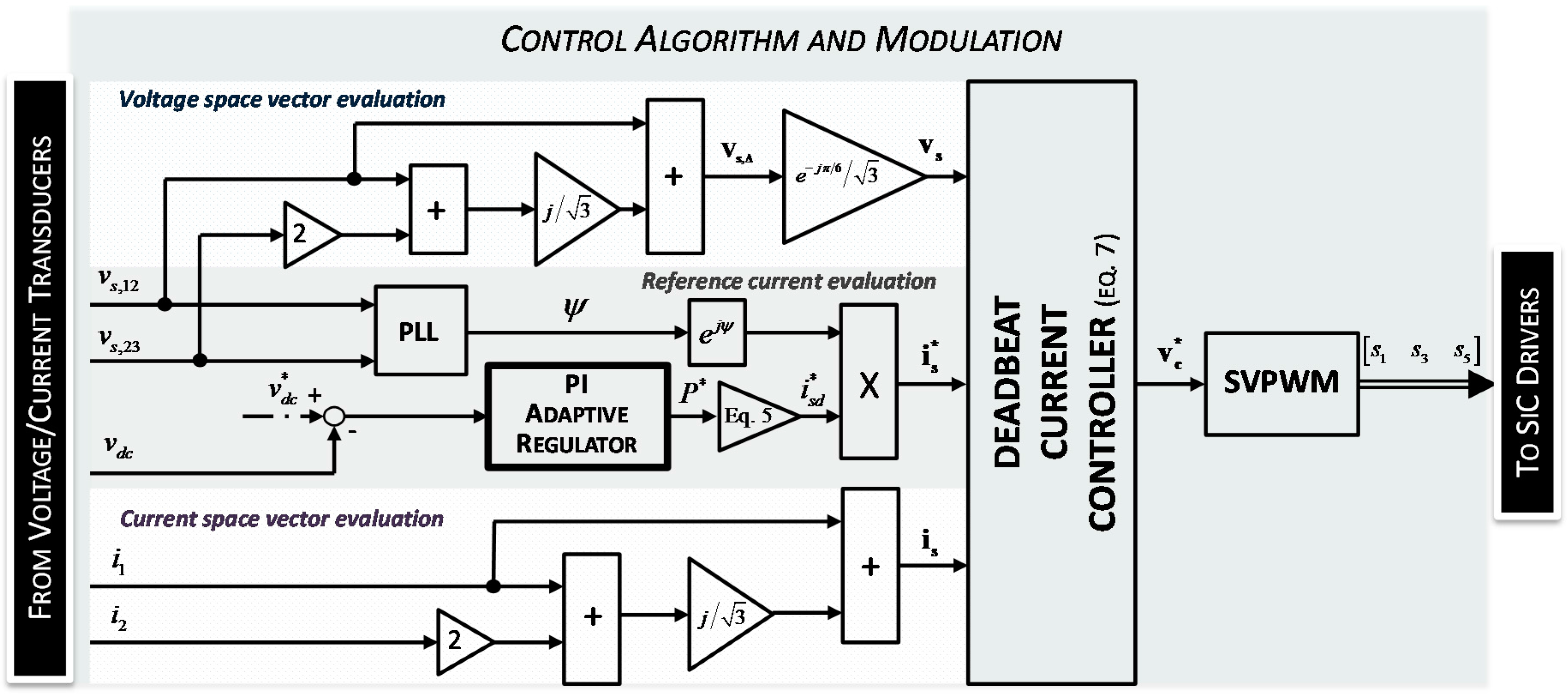
Figure 3.
behavior of the reference power ratio (a), the relative voltage error (b) and the proportional component (c).
Figure 3.
behavior of the reference power ratio (a), the relative voltage error (b) and the proportional component (c).
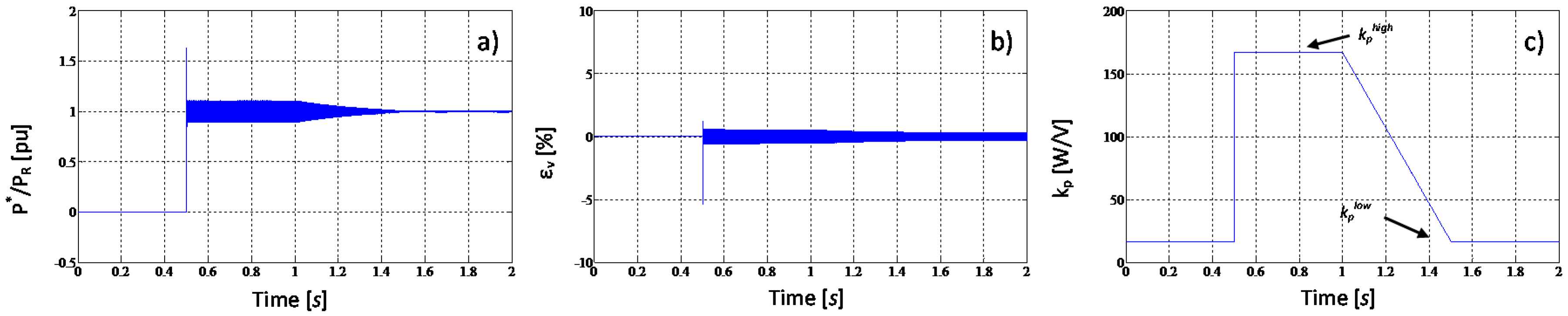
Figure 4.
DC-Link capacitance C behavior (a) and boost inductance L behavior (b) versus the line currents Total Harmonic Distortion (THD) expressed in percent [%].
Figure 4.
DC-Link capacitance C behavior (a) and boost inductance L behavior (b) versus the line currents Total Harmonic Distortion (THD) expressed in percent [%].

Figure 5.
Behaviors of the absorbed power P (a) and of the DC-Link voltage vdc (b) in the whole simulation interval.
Figure 5.
Behaviors of the absorbed power P (a) and of the DC-Link voltage vdc (b) in the whole simulation interval.
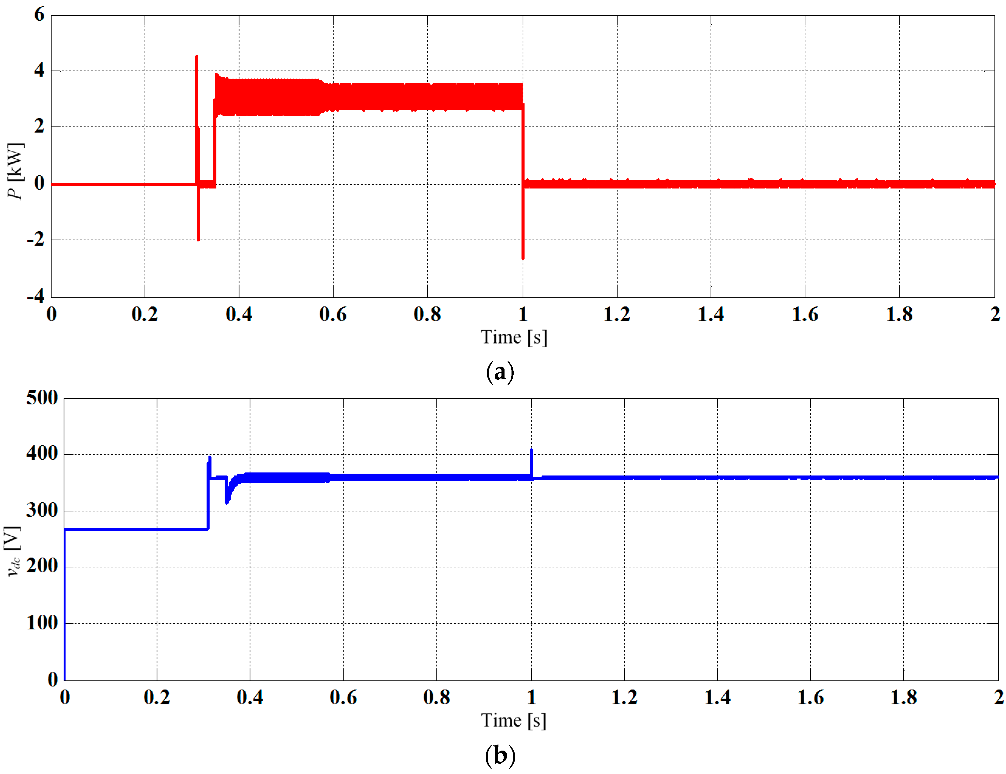
Figure 6.
Grid voltages (a) and line currents (b) behaviors in steady state condition at the rated power.
Figure 6.
Grid voltages (a) and line currents (b) behaviors in steady state condition at the rated power.


Figure 7.
SiC dissipated power Pj (a) and relative junction temperature Tj (b) behaviors.
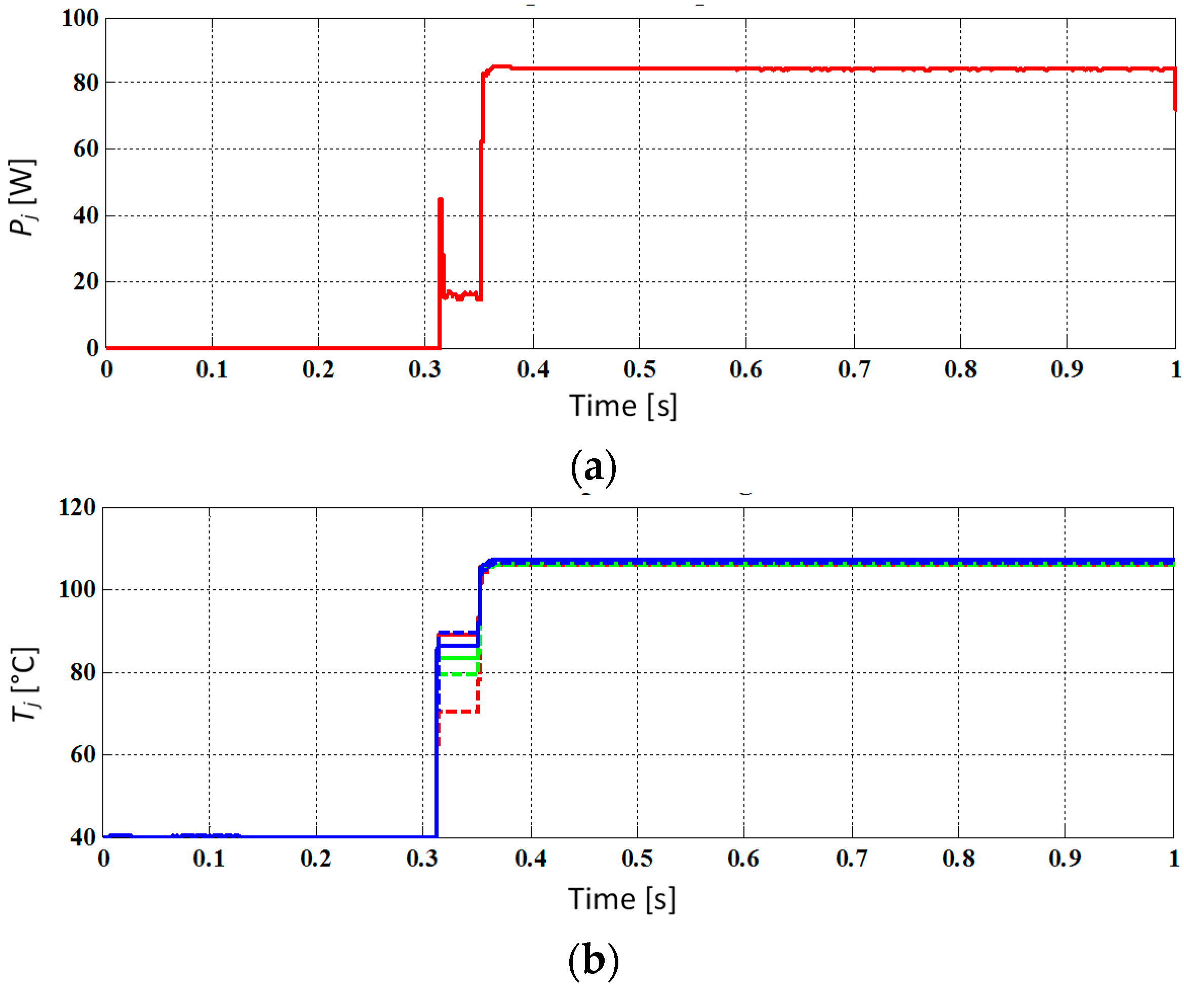
Figure 8.
PFC prototype and boost inductors.

Figure 9.
Behavior on the DC-Link voltage under different transient conditions: boost stage (a); 0→1.5 kW load step variation (b); 1.5→3 kW load step variation (c); 3 kW→0 load step variation (d).
Figure 9.
Behavior on the DC-Link voltage under different transient conditions: boost stage (a); 0→1.5 kW load step variation (b); 1.5→3 kW load step variation (c); 3 kW→0 load step variation (d).
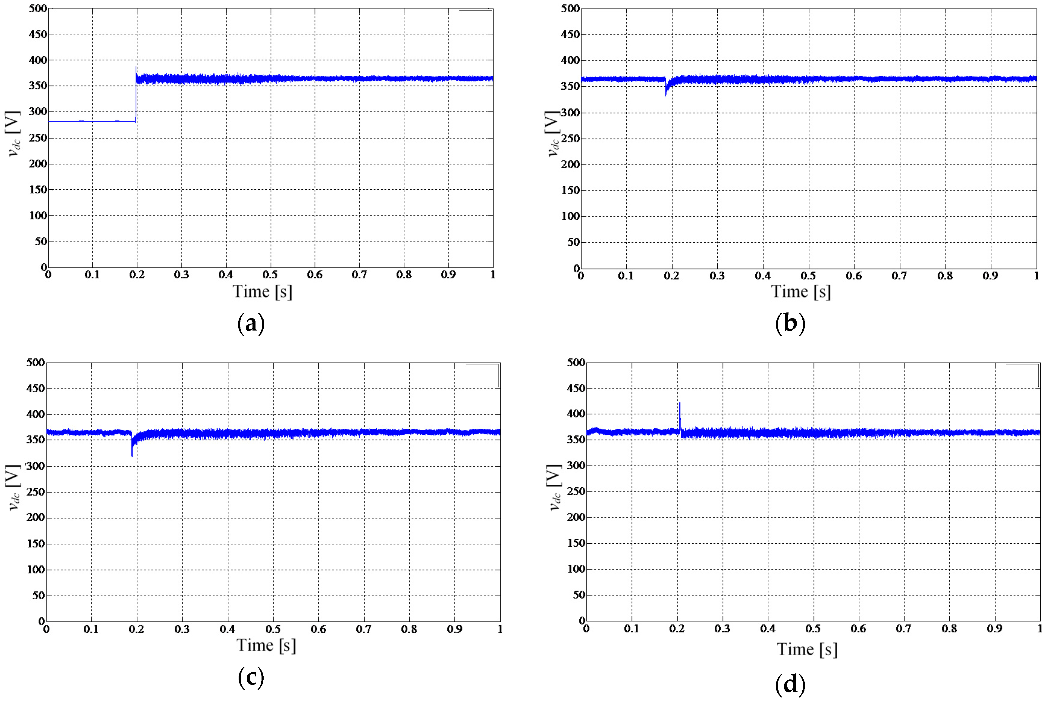
Figure 10.
Line current behaviors in steady state condition: 1.5 kW (a) and 3 kW (b).


Table 1.
Values of and for transient and steady state conditions.
| Transient Condition | Steady State Condition | ||
|---|---|---|---|
Table 2.
Main parameters of the simulated system.
| Quantity | Cree CCS020M12CM2 | Infineon FS25R12W1T4 |
|---|---|---|
| Overall Switching Energy (mJ) | 0.48 | 5.1 |
| On-Resistance (mΩ) | 80 | 90 |
| Rated Current at Tc = 100 °C (A) | 20 | 25 |
| Rated Voltage (kV) | 1.2 | 1.2 |
| Junction-Case Thermal Resistance (°C/W) | 0.75 | 0.7 |
Table 3.
Main parameters of the simulated system.
| Quantity | Symbol | Value |
|---|---|---|
| Grid rated voltage | 200 V | |
| Grid rated frequency | 400 Hz | |
| PFC rated power | 3 kW | |
| DC-Link rated voltage | 360 V | |
| PFC rated current | 9 A | |
| DC-Link capacitance | 75 µF | |
| Boost inductance | 2 mH | |
| Sampling time interval | 50 µs | |
| Switching frequency | 20 kHz |
© 2017 by the authors. Licensee MDPI, Basel, Switzerland. This article is an open access article distributed under the terms and conditions of the Creative Commons Attribution (CC BY) license (http://creativecommons.org/licenses/by/4.0/).
Share and Cite
MDPI and ACS Style
Brando, G.; Dannier, A.; Del Pizzo, A.; Coppola, M. An All-Electric-Aircraft Tailored SiC-Based Power Factor Correction Converter with Adaptive DC-Link Regulator. Energies 2017, 10, 1227. https://doi.org/10.3390/en10081227
AMA Style
Brando G, Dannier A, Del Pizzo A, Coppola M. An All-Electric-Aircraft Tailored SiC-Based Power Factor Correction Converter with Adaptive DC-Link Regulator. Energies. 2017; 10(8):1227. https://doi.org/10.3390/en10081227
Chicago/Turabian StyleBrando, Gianluca, Adolfo Dannier, Andrea Del Pizzo, and Marino Coppola. 2017. "An All-Electric-Aircraft Tailored SiC-Based Power Factor Correction Converter with Adaptive DC-Link Regulator" Energies 10, no. 8: 1227. https://doi.org/10.3390/en10081227
Note that from the first issue of 2016, this journal uses article numbers instead of page numbers. See further details here.