
On the Source of Oscillatory Behaviour during Switching of Power Enhancement Mode GaN HEMTs

Abstract
:1. Introduction
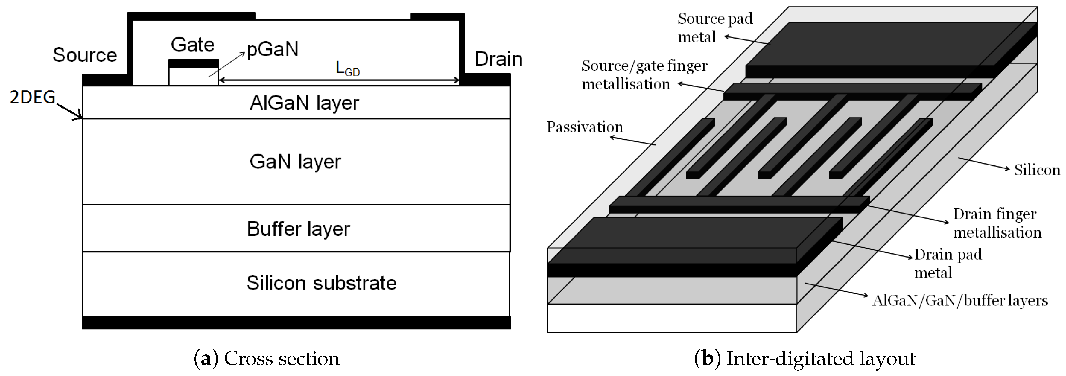
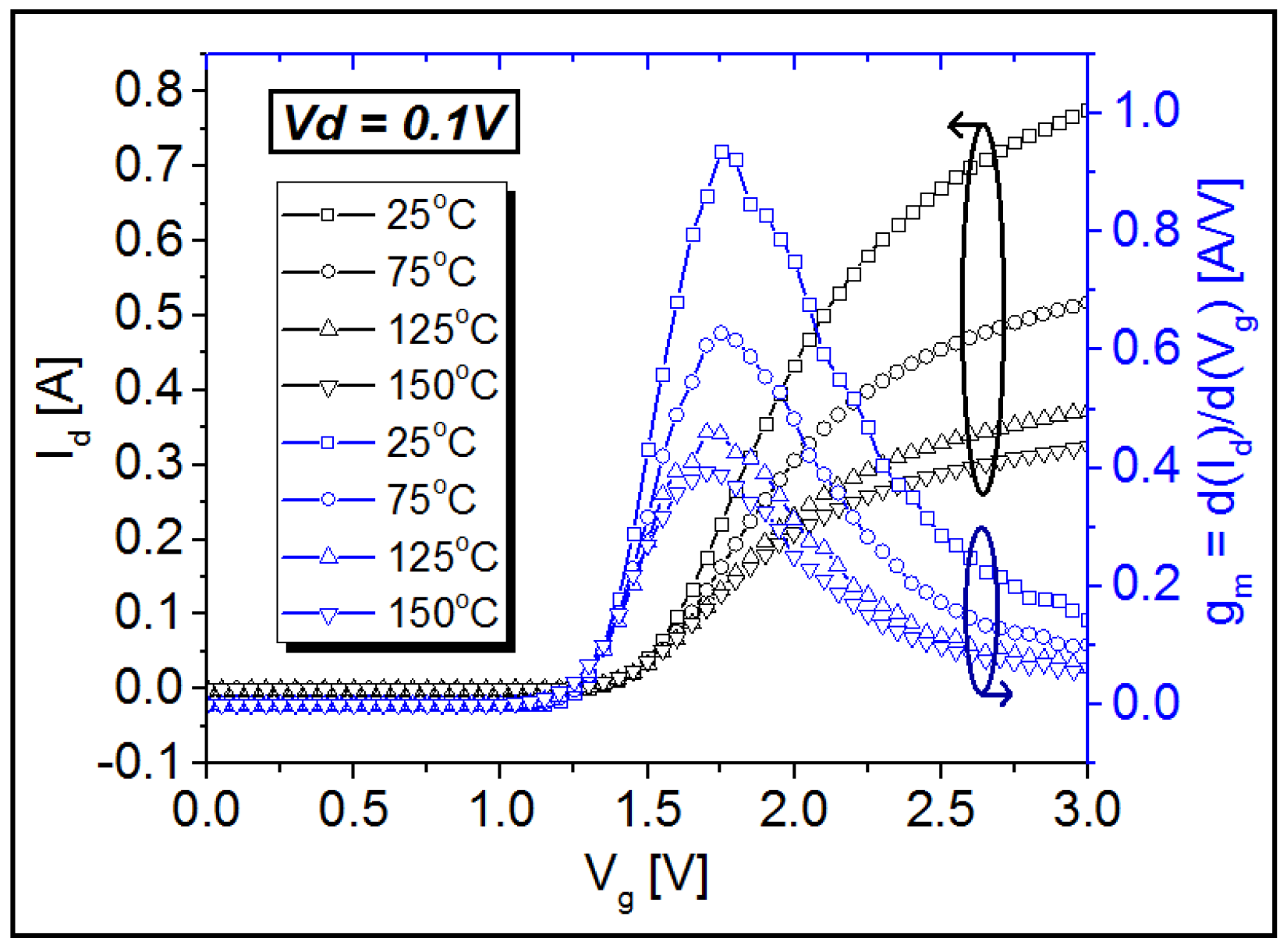
2. Device Structure and Characteristics
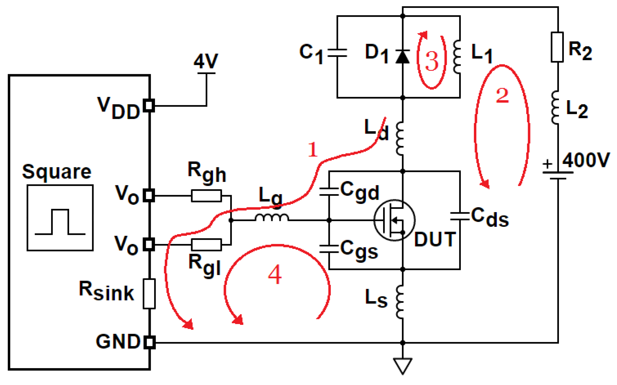
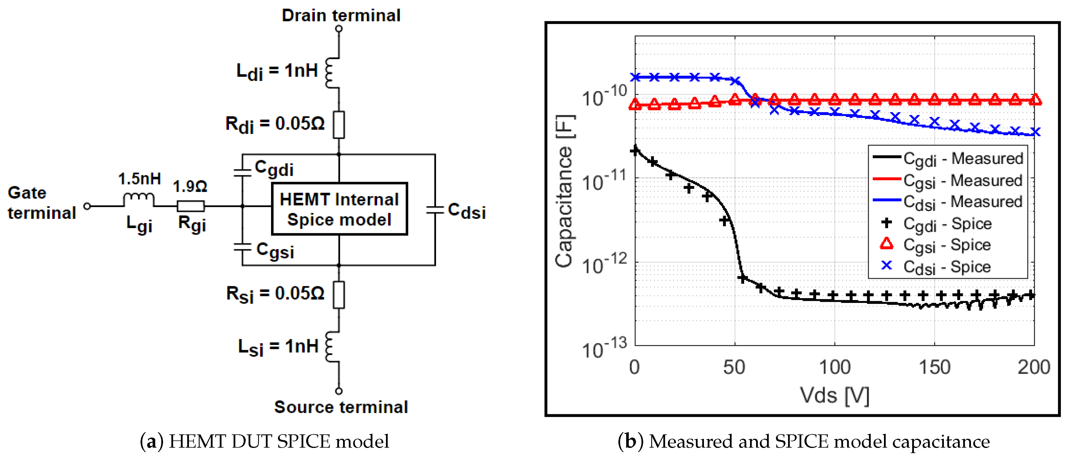
3. Experimental Method
4. Results and Discussion
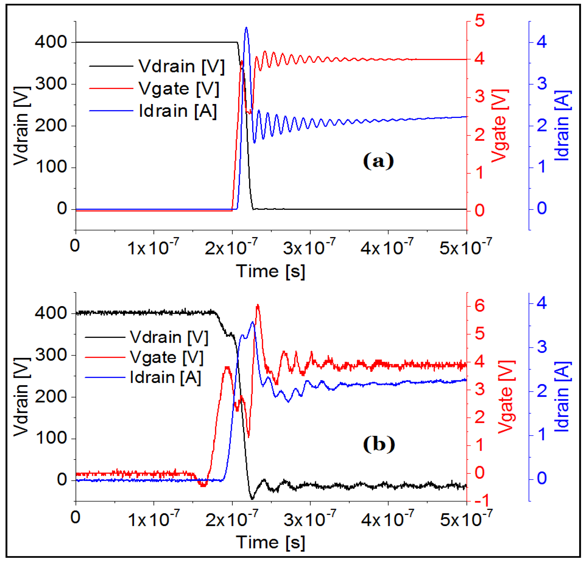
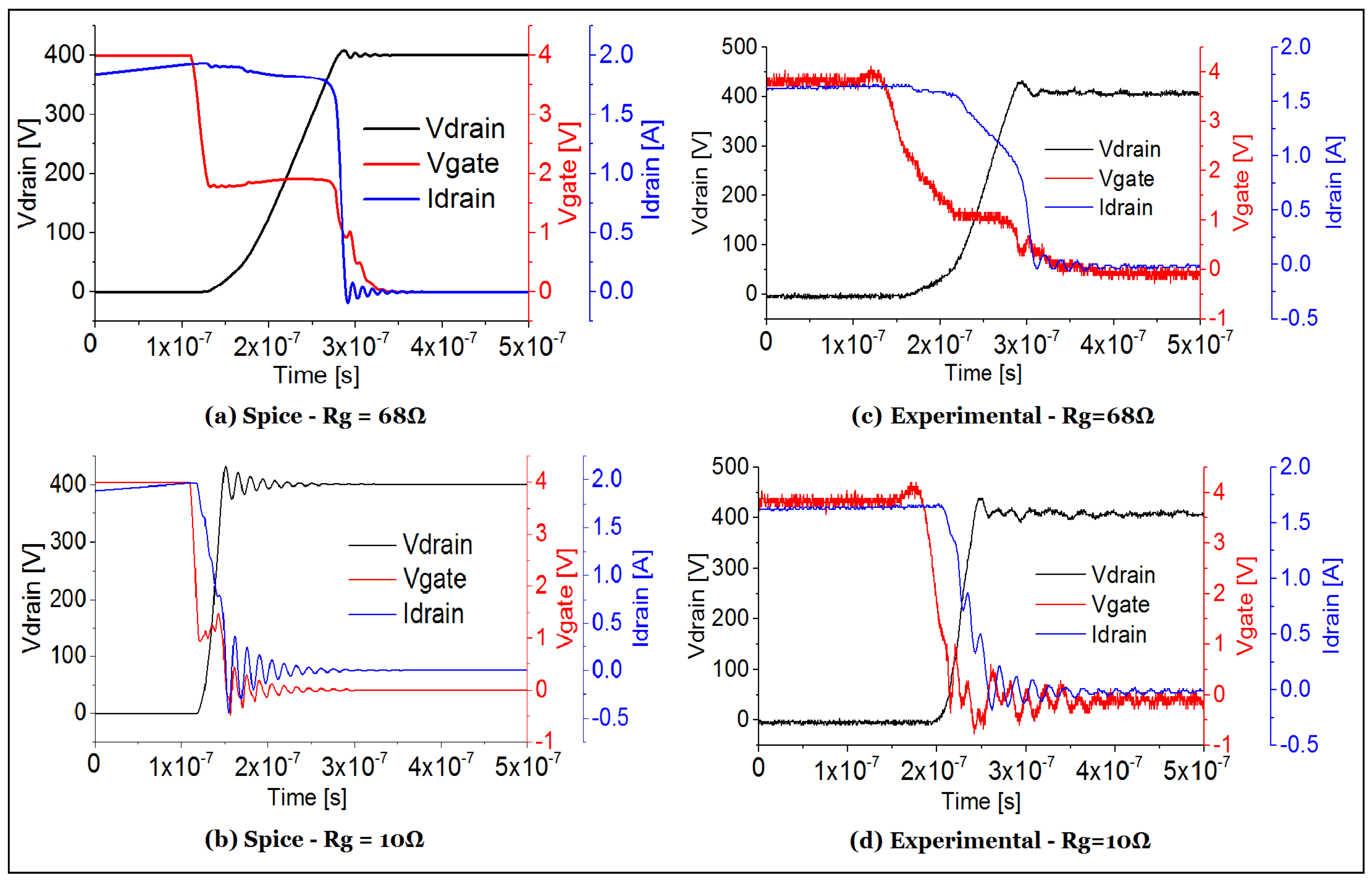
4.1. dV/dt Related Effect
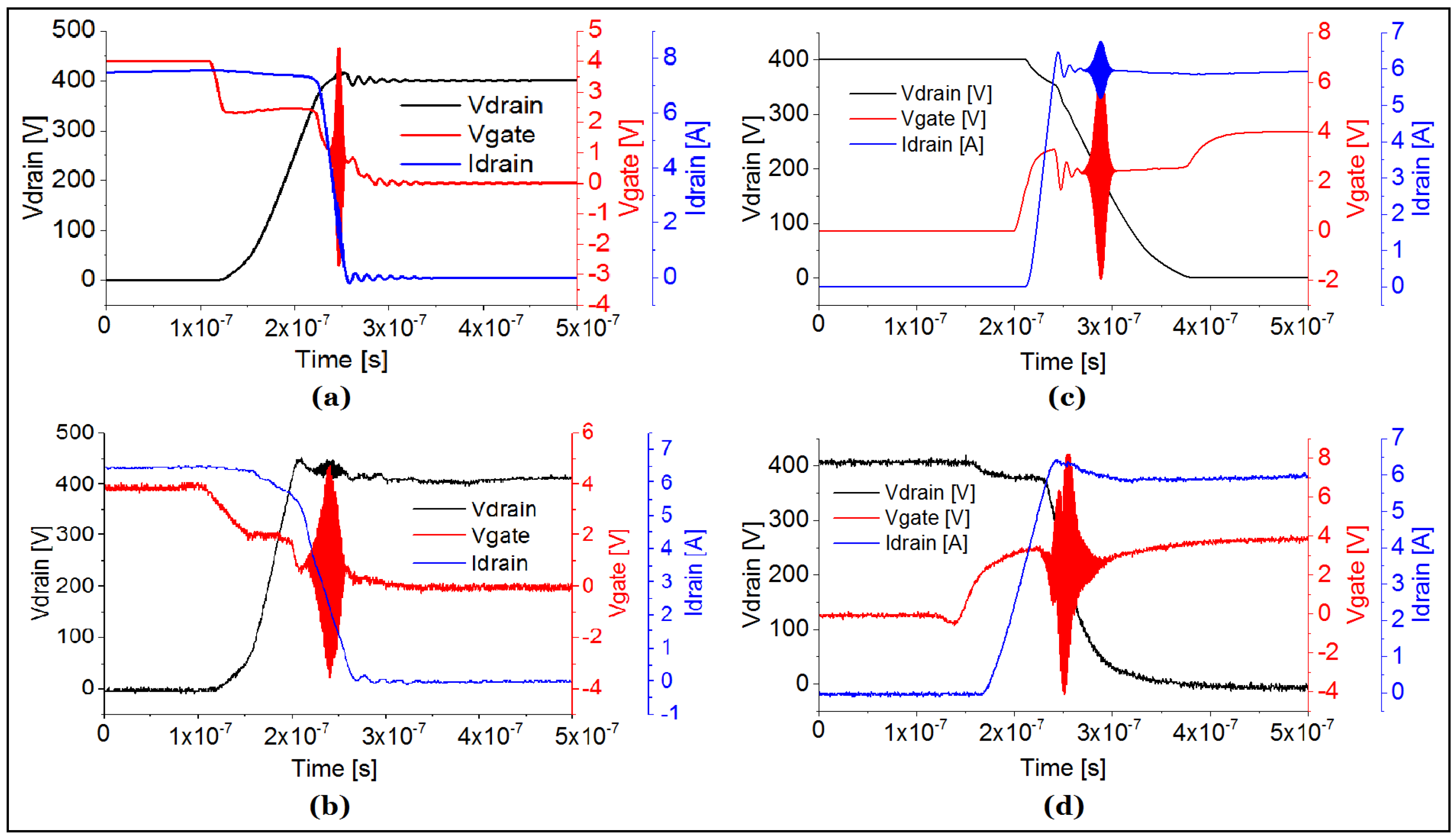
4.2. dI/dt Related Effect
Increased Temperature
4.3. Good Design Suggestions
4.3.1. Optimising Gate Drive Circuit to Address Related Ringing
- is high enough to control dV/dt, but not too high to generate a significant voltage drop when the discharge current of is flowing through. A trade-off is thus revealed. To allow stable switching the rate of switching of the device needs to be reduced however this can lead to increased losses.
- Smart driving is used such as an active Miller clamp function as seen in commercially available drivers (e.g. FOD8318, Fairchild, Sunnyvale, CA, USA). This function avoids a large discharge current flowing through by grounding the gate through the turn-on of a transistor when a certain voltage is developed across .
- Gate inductance is minimised as SPICE simulations reveal that gate inductance acts as to increase the amplitude of the oscillations observed. This is a result of the storage of energy when current is flowing through .
- The gate is driven to a negative voltage at turn-off to ensure unwanted device turn-on is avoided. This can however add cost and complexity to the design [16].
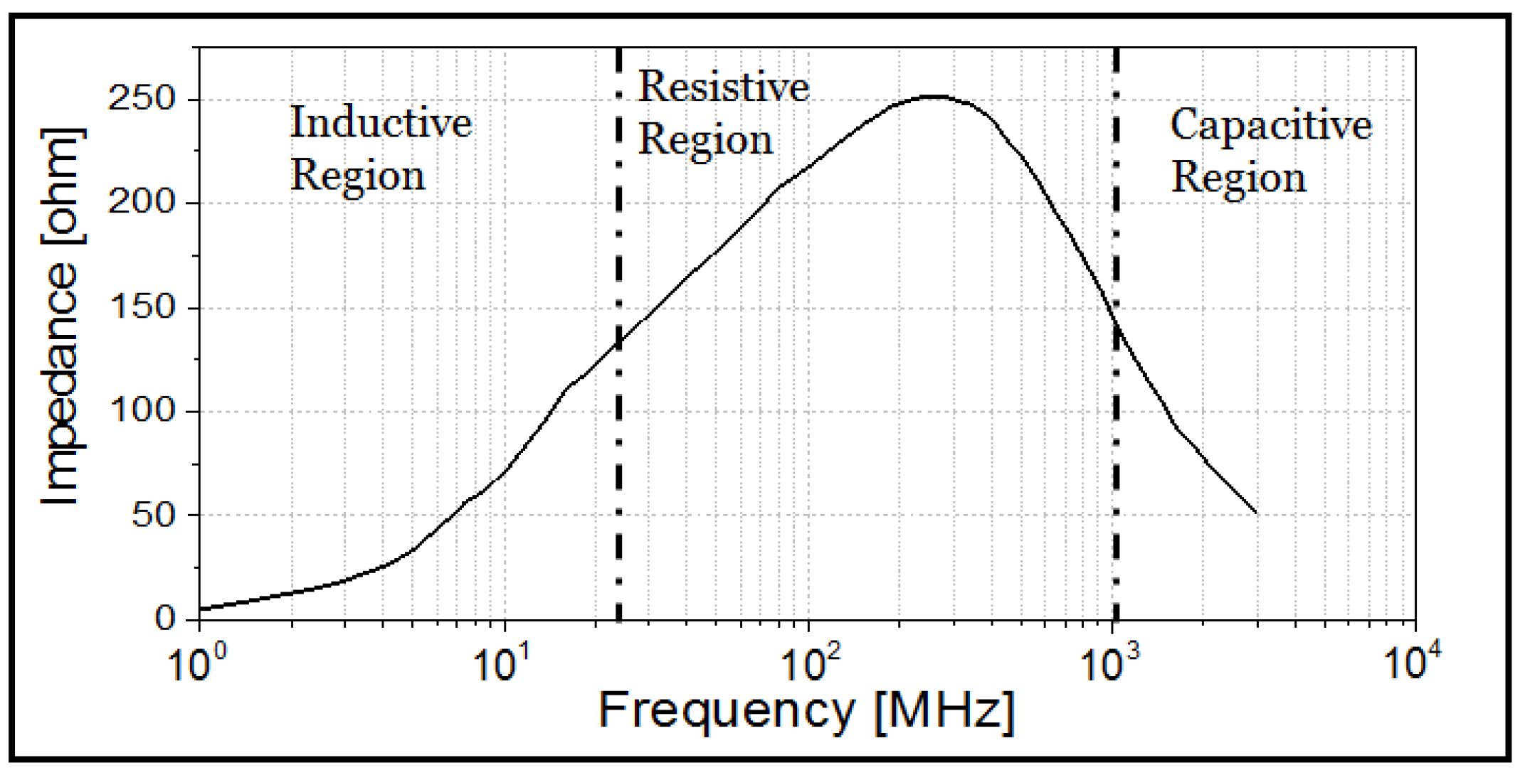
4.3.2. Use of Ferrite Bead to Address Related Ringing
5. Conclusions
Author Contributions
Conflicts of Interest
References
- Donkers, J.J.T.M.; Heil, S.B.S.; Hurkx, G.A.M.; Sonsky, J. 600V-900V GaN-on-Si Process Technology for Schottky Barrier Diodes and Power Switches Fabricated in a Standard Si-Production Fab. In Proceedings of the 16th CS MANTECH, New Orleans, LA, USA, 13–16 May 2013; pp. 259–262.
- Kwan, M.H.; Wong, K.-Y.; Lin, Y.S.; Yao, F.W.; Tsai, M.W.; Chang, Y.-C.; Chen, P.C.; Su, R.Y.; Wu, C.-H.; Yu, J.L.; et al. CMOS-Compatible GaN-on-Si Field-Effect Transistors for High Voltage Power Applications. In Proceedings of the 2014 IEEE International Electron Devices Meeting (IEDM), San Francisco, CA, USA, 15–17 December 2014; pp. 17–20.
- Jones, E.A.; Wang, F.; Costinett, D.; Zhang, Z.; Guo, B.; Liu, B.; Ren, R. Characterization of an enhancement-mode 650-V GaN HFET. In Proceedings of the IEEE Energy Conversion Congress and Exposition (ECCE), Montreal, QC, Canada, 20–24 September 2015; pp. 400–407.
- Morita, T.; Tamura, S.; Anda, Y.; Ishida, M.; Uemoto, Y.; Ueda, T.; Tanaka, T.; Ueda, D. 99.3% Efficiency of three-phase inverter for motor drive using GaN-based Gate Injection Transistors. In Proceedings of the 26th Annual IEEE APEC, Fort Worth, TX, USA, 6–11 March 2011; pp. 481–484.
- Mitova, R.; Ghosh, R.; Mhaskar, U.; Klikic, D.; Wang, M.X.; Dentella, A. Investigations of 600 V GaN HEMT and GaN Diode for Power Converter Applications. IEEE Trans. Power Electron. 2014, 29, 2441–2452. [Google Scholar] [CrossRef]
- Zdanowski, M.; Rąbkowski, J. Operation modes of the GaN HEMT in high-frequency half-bridge converter. In Proceedings of the Progress in Applied Electrical Engineering (PAEE), Koscielisko/Zakopane, Poland, 26 June–1 July 2016; pp. 1–6.
- Lu, J.; Bai, H.; Brown, A.; McAmmond, M.; Chen, D.; Styles, J. Design consideration of gate driver circuits and PCB parasitic parameters of paralleled E-mode GaN HEMTs in zero-voltage-switching applications. In Proceedings of the IEEE Applied Power Electronics Conference and Exposition (APEC), Long Beach, CA, USA, 20–24 March 2016; pp. 529–535.
- Lidow, A.; Strydom, J.; De Rooij, M.; Reusch, D. GaN Transistors for Efficient Power Conversion; John Wiley & Sons: Hoboken, NJ, USA, 2014; pp. 31–35. [Google Scholar]
- Efthymiou, L.; Camuso, G.; Longobardi, G.; Udrea, F.; Lin, E.; Chien, T.; Chen, M. Zero reverse recovery in SiC and GaN Schottky diodes: A comparison. In Proceedings of the 28th International Symposium on Power Semiconductor Devices and ICs (ISPSD), Prague, Czech Republic, 12–16 June 2016; pp. 71–74.
- Ambacher, O.; Smart, J.; Shealy, J.R.; Weimann, N.G.; Chu, K.; Murphy, M.; Schaff, W.J.; Eastm, L.F. Two dimensional electron gases induced by spontaneous and piezoelectric charges in N- and Ga-face AlGaN/GaN heterostructures. J. Appl. Phys. 1999, 85, 3222–3233. [Google Scholar] [CrossRef]
- Mishra, U.K.; Shen, L.; Kazior, T.E.; Wu, Y.-F. GaN-Based RF power devices and amplifiers. Proc. IEEE 2008, 96, 287–305. [Google Scholar] [CrossRef]
- Infineon 650V CoolMOS C7 Power Transistor IPL65R130C7. Available online: http://www.infineon.com/cms/en/product/productType.html?productType=db3a30443e78f08a013e795f46ad0157 (accessed on 17 March 2017).
- Hwang, I.; Choi, H.; Lee, J. 1.6 kV, 2.9 mΩ cm2 normally-off p-GaN HEMT device. Proc. ISPSD 2012, 24, 41–44. [Google Scholar]
- Lee, F.; Su, L.Y.; Wang, C.H.; Wu, Y.R.; Huang, J. Impact of gate metal on the performance of p-GaN/AlGaN/GaN High electron mobility transistors. IEEE Electron Device Lett. 2015, 36, 232–234. [Google Scholar] [CrossRef]
- Jones, E.A.; Wang, F.; Costinett, D.; Zhang, Z.; Guo, B. Temperature-dependent turn-on loss analysis for GaN HFETs. In Proceedings of the 2016 IEEE Applied Power Electronics Conference and Exposition (APEC), Long Beach, CA, USA, 20–24 March 2016; pp. 1010–1017.
- GN001 Application Note, How to Drive GaN E-Mode Transistors, 2014-10-21. Available online: http://www.gansystems.com/_uploads/whitepapers/982304_GN001%20App%20Note%20-%20How %20to%20Drive%20GaN%20E-Mode%20Transistors%202014-10-21.pdf (accessed on 17 March 2017).
- Eco, J.; Limjoco, A. Ferrite Bead Demystified. Application Note AN-1368. Available online: http://www.analog.com/media/en/technical-documentation/application-notes/AN-1368.pdf (accessed on 17 March 2017).
- Tai Tech Advanced Electronics Ferrite Core, Model No: LF-W5 T 3.5*0.8*1.6+C. Available online: http://www.tai-tech.com.tw/product/product.php?lang=zh-TW&c=102&s=201&p=217 (accessed on 17 March 2017).
- Wurth Elektronik Ferrite Core, Model No: 742 792 711 2. Available online: http://katalog.we-online.com/en/midcom/ (accessed on 17 March 20017).


© 2017 by the authors. Licensee MDPI, Basel, Switzerland. This article is an open access article distributed under the terms and conditions of the Creative Commons Attribution (CC BY) license ( http://creativecommons.org/licenses/by/4.0/).
Share and Cite
Efthymiou, L.; Camuso, G.; Longobardi, G.; Chien, T.; Chen, M.; Udrea, F. On the Source of Oscillatory Behaviour during Switching of Power Enhancement Mode GaN HEMTs. Energies 2017, 10, 407. https://doi.org/10.3390/en10030407
Efthymiou L, Camuso G, Longobardi G, Chien T, Chen M, Udrea F. On the Source of Oscillatory Behaviour during Switching of Power Enhancement Mode GaN HEMTs. Energies. 2017; 10(3):407. https://doi.org/10.3390/en10030407
Chicago/Turabian StyleEfthymiou, Loizos, Gianluca Camuso, Giorgia Longobardi, Terry Chien, Max Chen, and Florin Udrea. 2017. "On the Source of Oscillatory Behaviour during Switching of Power Enhancement Mode GaN HEMTs" Energies 10, no. 3: 407. https://doi.org/10.3390/en10030407
APA StyleEfthymiou, L., Camuso, G., Longobardi, G., Chien, T., Chen, M., & Udrea, F. (2017). On the Source of Oscillatory Behaviour during Switching of Power Enhancement Mode GaN HEMTs. Energies, 10(3), 407. https://doi.org/10.3390/en10030407