Article

Novel Three-Phase Nine-Level Inverter and Its Control Strategies

1
Electrical Engineering Department, École Supérieure de Technologie (ESTM), Moulay Ismail University, Meknes 50000, Morocco
2
École de Technologie Supérieure (ETS), Montreal, QC 11290, Canada
*
Author to whom correspondence should be addressed.
Electronics 2022, 11(20), 3348; https://doi.org/10.3390/electronics11203348
Submission received: 25 July 2022 / Revised: 28 September 2022 / Accepted: 29 September 2022 / Published: 17 October 2022
(This article belongs to the Section Power Electronics)

Abstract

:
In this paper, the authors propose a new three-phase, nine-level inverter with self-balancing of capacitors voltages. The proposed inverter is the result of a serial connection of the SPUC topology and the NPC converter. A single DC source is used, and each phase is made up of nine power switches and three capacitors. Two control techniques are proposed to maintain capacitors voltages at desired values, the first of which is a PWM technique ensures the self-balancing of capacitors voltages in open loop without using any filters or PI regulators, and the second is based on the hysteresis control which offers a nearly sinusoidal waveform of the load current without using any voltage sensors. The authors make use of the Matlab Simulink environment to perform the simulation of the proposed concept. The dynamics of the latter was verified against load change.

1. Introduction

In recent years, multilevel inverters have attracted considerable attention because of their advantages, including low electromagnetic interference (EMI), reduced voltage stress (dv/dt), low total harmonics distortion (THD), and high power conversion.
Many three-phase inverters were proposed over the years. Most of them are based on the three basic topologies, which are the neutral point clamped (NPC) [1], the cascaded H-bridge (CHB) [2], and the flying capacitor (FC) [3]. However, their power quality remains fairly low. The authors propose a solution by optimizing the number of active and passive devices. The proposed converter overcomes the serious drawback of the NPC by permitting a natural self-balancing of capacitors voltages when the number of the desired voltage levels is greater than three.
In this paper, we propose an advanced three-phase, nine-level inverter which is derived from the series connection of the SPUC [4] converter that allows a load voltage with high level number while using an optimized count of active and passive components and NPC topology that has the advantage of joining capacitors together. The proposed inverter uses the benefit of redundant states to perform the self-balancing of capacitors voltages in open loop without using any filters or PI regulators [5,6,7].
Firstly, a PWM technique is applied to the proposed inverter, as a result the system offering nine levels in output voltage without using any closed loop regulation [8,9,10,11,12,13,14,15,16,17,18,19]; because the latter is not suitable for some industrial applications, this allows a low cost of inverter and installation. Secondly, a hysteresis control is used to provide a near sinusoidal without the use of a voltage sensor or PI controllers.

2. Methods

Firstly, the proposed inverter topology, which is based on PUC and NPC converters, is presented in single- and three-phase versions, and then capacitors balancing techniques are detailed, which are PWM techniques and hysteresis controls.

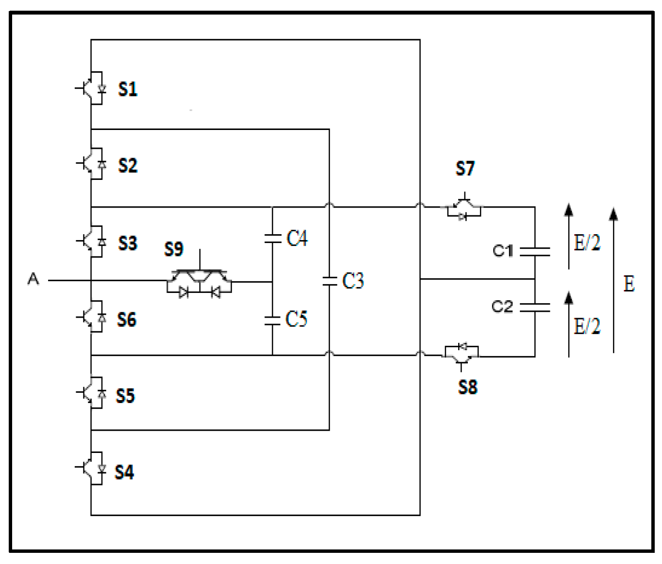
2.1. Presentation the Proposed Three-Phase Inverter Topology and Switching States

The proposed inverter is derived from a series connection of SPUC and NPC converters, and this connection was used between PUC and NPC converters [20]. As a result, it can provide a maximum of levels using a single DC source because a closed loop is used to keep voltage values of the desired capacitors.
The proposed topology has a new advantage, which is the ability to maintain capacitors voltages at desired values in open loop without any PI regulators and with two different methods of control, which are PWM techniques and hysteresis control. The proposed nine-level inverter is constituted from nine power switches and three capacitors per phase. Those capacitors, which are C3, C4, and C5 should be balanced respectively to E/2, E/8, and E/8. However, C1 and C2 should be maintained in the half of the DC source. Figure 1 represents the single phase of the nine-level inverter proposed.
In order to generate a nine level output voltage, we assume that Vc1 = Vc2 = Vc3i = E/2 and Vc4i = Vc5i = E/8 (i = a, b, c). Table 1 represents the nine required levels with redundant states (1′, 3′, 5′, 7, 9′). Figure 2 represents the three-phase, nine-level inverter proposed.
The nine levels were generated as follows.
In state 9, in which the load voltage is equal to Vc2, switches S6 and S8 are “ON”. Capacitor C2 is discharging since it is connected only to the load.
In state 8, in which the load voltage is equal to Vc3i − Vc5i, switches S1, S5, and S9 are “ON”. Capacitor C5 has a serial connection with capacitor C3, thus Capacitor 5 is charging. However, Capacitor 3 is discharging.
In state 7′, in which the load voltage is equal to Vc4i + Vc5i, switches S1, S2, and S6 are “ON”. Capacitors are connected directly to the load, so they are discharging.
In state 6, in which the load voltage is equal to Vc4i, switches S1, S2, and S9 are “ON”. Capacitor C4 is discharging since it is connected only to the load.
In state 5, in which the load voltage is equal to zero, switches S1, S2, and S3 are “ON”. There is no effect to capacitors since none is connected to the DC source.
In state 4, in which the load voltage is equal to −Vc5i, switches S4, S5, and S9 are “ON”. Capacitor C5 is discharging since it is connected only to the load.
In state 3, in which the load voltage is equal to −Vc4i − Vc5i, switches S3, S4, and S5 are “ON”. Capacitors are connected directly to the load, thus, they are discharging.
In state 2, in which the load voltage is equal to Vc4i − Vc3i, switches S2, S4, and S9 are “ON”. Capacitor C4 has a serial connection with capacitor C3, thus, Capacitor 4 is charging. However, Capacitor 3 is discharging.
In state 1, in which the load voltage is equal to −Vc1, switches S3 and S7 are “ON”. Capacitor C1 is discharging since it is connected only to the load.
The number of voltage levels should be decreased in order to create several redundant states. The ability of choosing among them is one of the major advantages. Indeed, a state can be chosen according to the desired charging or discharging capacitor behavior while keeping the same output voltage value. As shown in Table 1, states (3 and 3′) allow the same output voltage, which is equal to −200 V. One can proceed by the same manner to determine the other redundant states.

2.2. Proposed Nine-Level Inverter Using PWM Technique

In order to generate the gate pulses, one has to design a modulation technique. Consequently, in this paper, the authors propose the following procedure in which a sign function of the reference voltage is used to determine S 1 .
Sign v r = 1 , v r 0 0 , v r < 0
S 1 = Sign v r
Eight equal amplitude triangular carriers which are indicated by the letter C ri (i = 1…8) are compared with the sinusoidal reference, the carriers arrangements for PWM strategy are shown in Figure 3, and each comparison generates a new signal indicated by the letter Zi (i = 1…8).
Z 1 = 1 , C r 1 v r 0 , C r 1 < v r
Z 2 = 1 , C r 2 v r 0 , C r 2 < v r
Z 3 = 1 , C r 3 v r 0 , C r 3 < v r
Z 4 = 1 , C r 4 v r 0 , C r 4 < v r
Z 5 = 1 , C r 5 v r 0 , C r 5 < v r
Z 6 = 1 , C r 6 v r 0 , C r 6 < v r
Z 7 = 1 , C r 7 v r 0 , C r 7 < v r
Z 8 = 1 , C r 8 v r 0 , C r 8 < v r
A staircase signal which the image of the voltage load can then be generated by summing these equations is as follows.
S = Z 1 + Z 2 + Z 3 + Z 4 + Z 5 + Z 6 + Z 7 + Z 8
The remaining gate pulses can then be expressed as follows.
S 2 = S 5 ¯
S 3 = Z 6 ¯ + Z 8 ¯
S 4 = 1     sign ( v r )
S 5 = ( Z 1 Z 2 Z 3 Z 4 ) + ( Z 1 Z 2 Z 3 Z 4 )
S 6 = Z 1 + Z 3 + ( Z 4 Z 5 )
S 7 = ( Z 1 Z 2 ) + ( Z 3 Z 4 ) + ( Z 5 Z 6 ) + ( Z 7 Z 8 )
S 8 = Z 1
S 9 = Z 8
Finally, the proposed control technique is depicted in Figure 4. It permits the self-balancing of capacitors voltages in open loop operation.

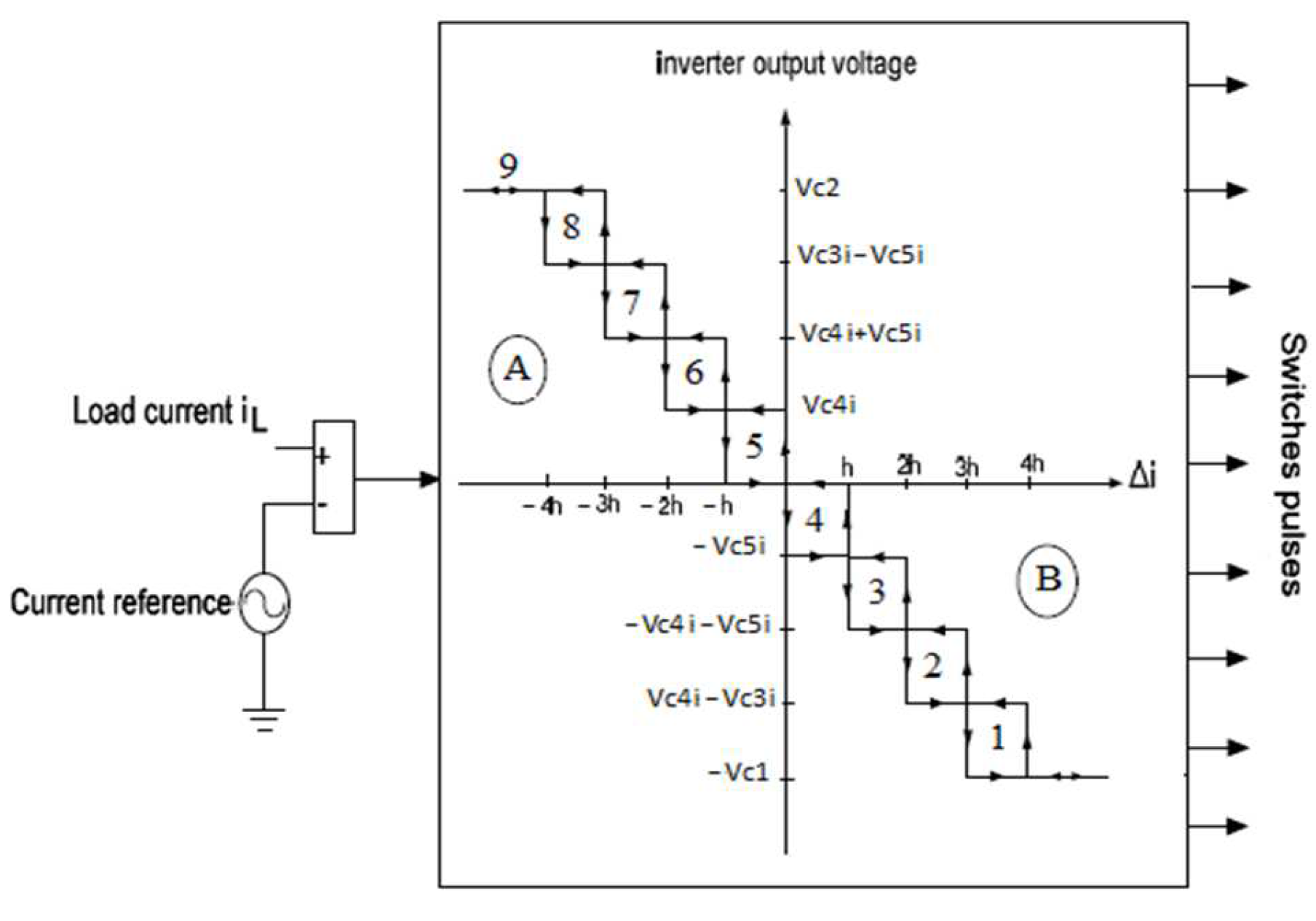
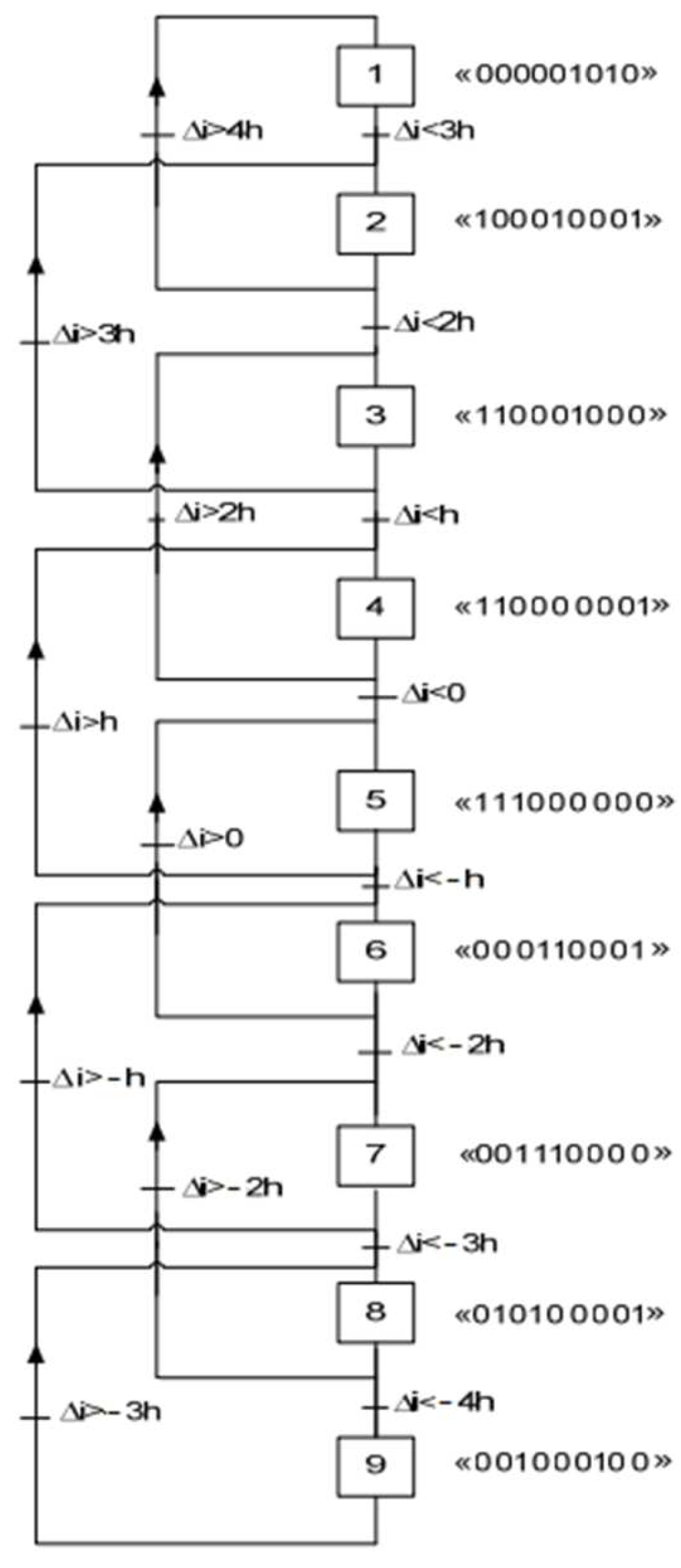
2.3. Proposed Nine-Level Inverter Using Hysteresis Control

The proposed control technique is based on the eight band hysteresis approach, when the current error Δi is negative. The positive voltages (sector A in Figure 5) are applied. Inversely, the negative voltages (sector B) are applied when the current error is positive. Δi is the difference between actual load current and its reference.
The nine states and their transition conditions are depicted in Figure 6. Switch pulses are presented in the following order S1i. S2i. S3i. S4i. S5i. S6i. S7i. S8i. S9i (i = a, b, c).

3. Results

Simulation of the proposed SPUC-NPC three-phase, nine-level inverter was carried out in the MATLAB/SIMULINK environment.

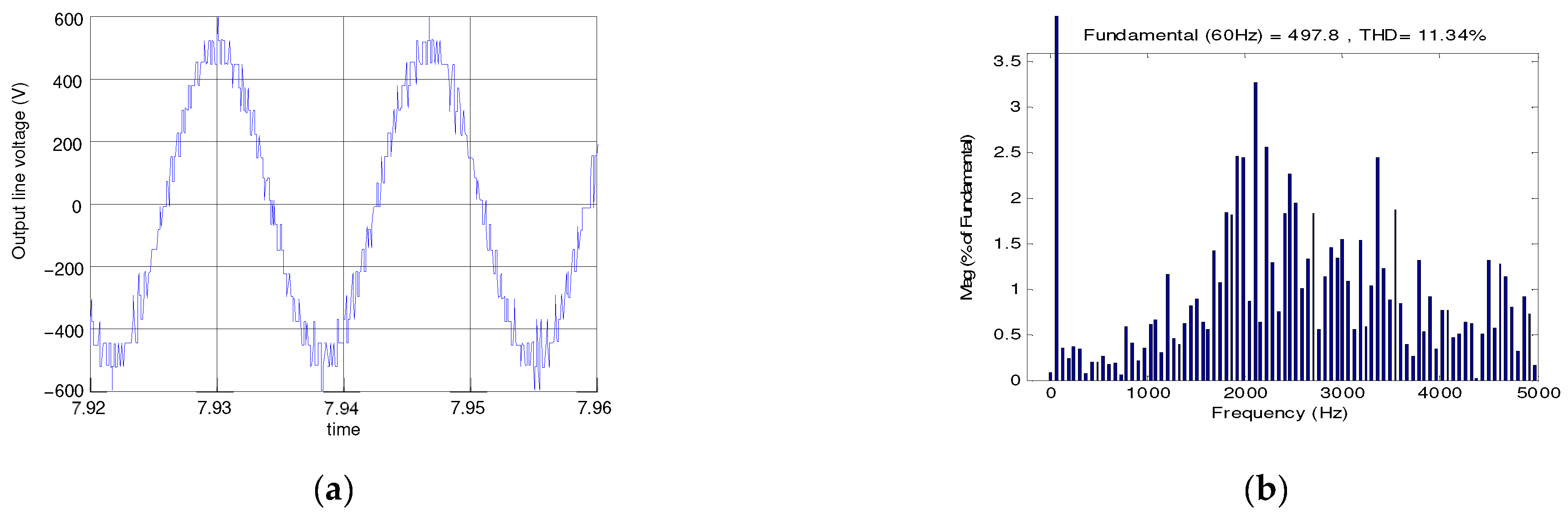
3.1. Using PWM Technique

The parameters used for the simulation are presented in Table 2:
As shown in Figure 7, capacitors voltages are respectively well balanced and remain in steady state around the half of the DC source voltage for Vc1 and Vc2. However capacitor voltages of the three phases (a, b, and c) which are Vc3i, Vc4i, and Vc5i (i = a, b, c) are maintained in E/2 for capacitor 3 and the eighth of the DC source for capacitors 4 and 5.
Figure 8a shows the inverter output voltage waveform. The latter is constituted of nine voltage levels, which are {400 V; 300 V; 200 V; 100 V; 0; −100 V; −200 V; −300 V; −400 V}. However, the load current is nearly sinusoidal as is presented in Figure 8c. This waveform is obtained without using any active or reactive filter. Moreover, no sensor or closed loop is used, which permits a low inverter and installation cost.
A very low THD is achieved. The THD level of the proposed three-phase, nine-level inverter is 16.36% for output voltage (Figure 8b) and 4.39% for output current waveform (Figure 8d). Although this value fulfills standards, it can be reduced by increasing the modulating signal frequency or amplitude modulation index, and to prove this, another simulation is done using 2000 Hz as the switching frequency, with the other parameters kept at the same values; Figure 9 shows simulation results.
The proposed concept is verified against a load resistance change. Therefore, at t = 5 s, load resistance changes from 30 Ω to 15 Ω. Other parameters keep the same values, which are 800 V for DC link and 15 mH for load inductance.
Simulation results show that capacitors voltages keep the same values, even after a severe load change. In fact, Vc1 and Vc2 are fixed in the half of the DC source. However, others capacitors remain well maintained around the half of the DC link for Vc3i and the eighth of the DC source for Vc4i and Vc5i (i = a, b, c). Figure 10 shows capacitors voltages against step load change.
The load voltage behavior before and after load change is depicted in Figure 11a. The balancing technique operates very well even during load change. Figure 11b shows load current behavior before and after load change. The current remains nearly sinusoidal even during load change, which reflects the high dynamics of the proposed algorithm.

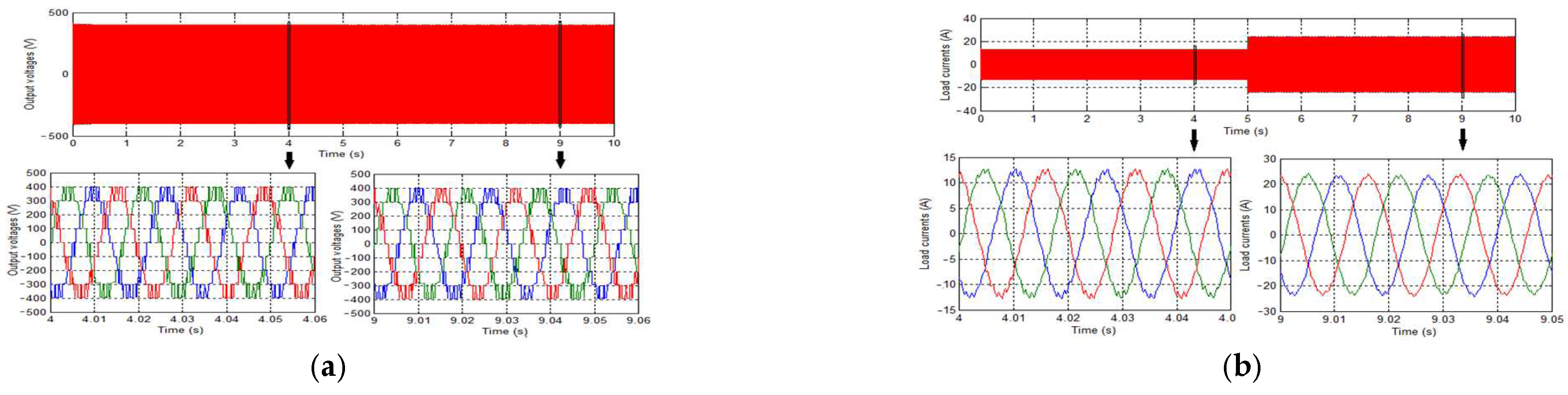
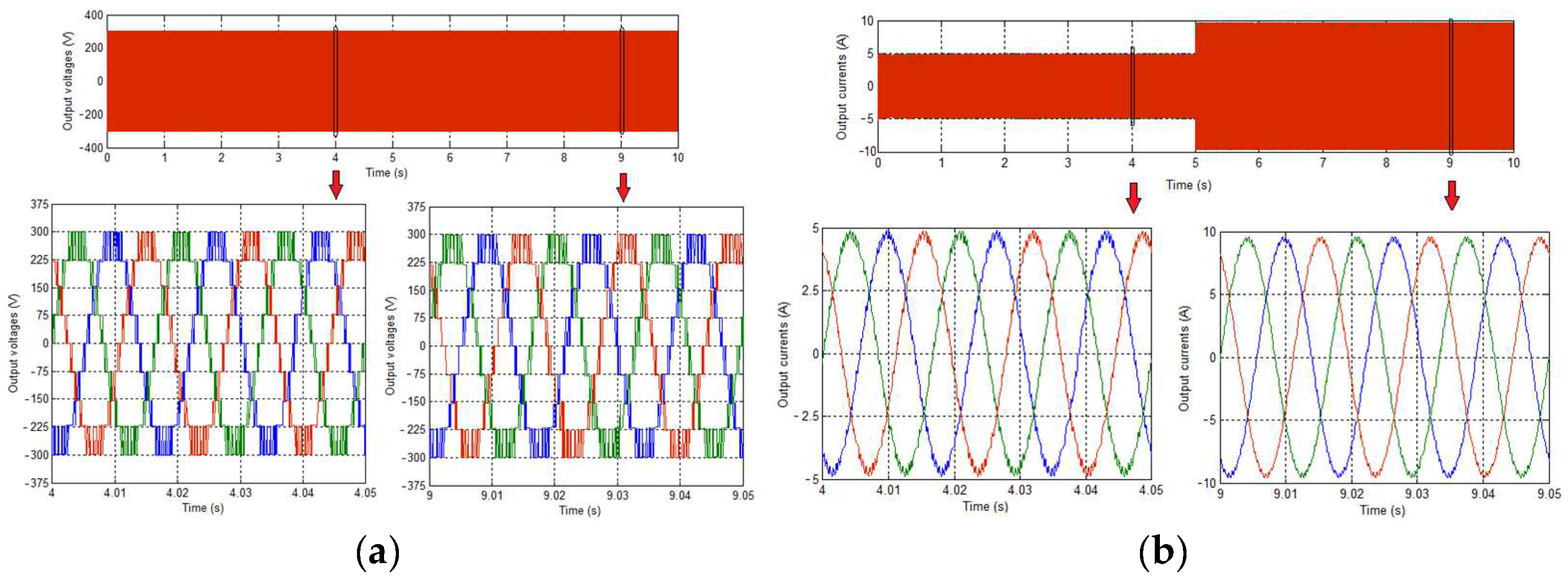
3.2. Using Hysteresis Control

Simulation was performed using parameters depicted in Table 3.
As shown in Figure 12, the capacitors are seen to have reached their desired voltage values, thus Vc1 and Vc2 are fixed around the half of the DC source. However, Vc3i, Vc4i, and Vc5i (i = a, b, c) are balanced, respectively, to E/2, E/8, and E/8. The same results are obtained for the three phases. No voltage sensor or closed loop is needed.
As shown in Figure 13a, the output voltage consists of nine voltage levels, and 15.19% is the THD level detected as being presented in Figure 13b. However, the load current is nearly sinusoidal as is presented in Figure 13c, with 1.96% as THD level (Figure 13d), the output line-to-line voltage and its THD level are presented in Figure 14.These waveforms are obtained without using any active or reactive filter. Moreover, no voltage sensor or PI regulator is used which permits a low inverter and installation cost. The THD level can be reduced by reducing the hysteresis bandwidth. The nine switching patterns are presented in Figure 15.
In order to verify the high dynamics of the proposed system, a load resistance change is applied at t = 5 s. In fact, resistance is changed from 60 Ω to 30 Ω. Other parameters keep the same values.
Capacitors voltages are well maintained around the desired value, even after a severe load change. In fact Vc1 and Vc2 are fixed in the half of the DC source. However, other capacitors are maintained around the half of the DC link for Vc3i and the eighth of the DC source for Vc4i and Vc5i (i = a, b, c). Figure 16 shows the capacitors voltages against step load change.
As shown in Figure 17, before and after the change, the load voltage is constituted of nine levels with the same step, which is 75 V. By the same way, load current is nearly sinusoidal before and after the change, which reflects the high dynamics of the proposed system.

4. Comparative Study

Table 4 compares the THD level of output voltage with other topologies by varying the switching frequency and amplitude modulation index, and we observe that the proposed topology has a low THD level without the need of any filters; however, Table 5 presents a comparison of switching components, and the comparison includes basic topologies and the PUC inverter, as can be seen, the SPUC-NPC three-phase, nine-level inverter has a significant advantage other than the use of a limited number of power components, which is the implementation of one DC source, and other capacitors voltages are balanced without the use of any closed loop regulation and with two control methods, which are PWM techniques and hysteresis control.

5. Conclusions

A novel three-phase inverter using only nine power switches and three capacitors per phase has been presented in this paper. The proposed topology is able to generate nine levels at the output voltage while using a single DC source. The self-balancing of capacitors voltages is achieved with two control methods, which are PMM techniques and hysteresis control. No filters or PI regulators are used, which permits a low inverter and installation cost. The high dynamics of the proposed inverter was verified by simulation.

Author Contributions

Conceptualization, A.E.G. and Y.O.; methodology, A.E.G.; software, A.E.G.; validation, H.E.O., Y.O. and K.A.-h.; formal analysis, A.E.G.; investigation, Y.O.; resources, A.E.G. and Y.O.; data curation, A.E.G.; writing—original draft preparation, A.E.G.; writing—review and editing, Y.O. All authors have read and agreed to the published version of the manuscript.

Funding

This research was funded by École de Technologie Supérieure (ETS), Montreal, Canada.

Data Availability Statement

Not applicable.

Conflicts of Interest

The authors declare no conflict of interest.

References

  1. Nabae, A.; Takahashi, I.; Akagi, H. A New Neutral-Point-Clamped PWM Inverter. IEEE Trans. Ind. Appl. 1981, IA-17, 518–523. [Google Scholar] [CrossRef]
  2. Peng, F.Z.; Lai, J.-S.; McKeever, J.W.; VanCoevering, J. A multilevel voltage-source inverter with separate DC sources for static VAr generation. IEEE Trans. Ind. Appl. 1996, 32, 1130–1138. [Google Scholar] [CrossRef] [Green Version]
  3. Meynard, T.A.; Foch, H. Multi-level conversion: High voltage choppers and voltage-source inverters. In Proceedings of the PESC’92 Record, 23rd Annual IEEE Power Electronics Specialists Conference, Toledo, Spain, 29 June–3 July 1992; pp. 397–403. [Google Scholar] [CrossRef]
  4. El Gadari, A.; el Ouardi, H.; Alibou, S.; Ounejjar, Y.; Bejjit, L.; Sharifzadeh, M.; Al-Haddad, K. New Nine-Level SPUC Inverter Using Single DC Source. In Proceedings of the IECON 2019—45th Annual Conference of the IEEE Industrial Electronics Society, Lisbon, Portugal, 14–17 October 2019. [Google Scholar] [CrossRef]
  5. Ounejjar, Y.; Al-Haddad, K. New Nine-Level Inverter with Self Balancing of Capacitors Voltages. In Proceedings of the IECON 2018—44th Annual Conference of the IEEE Industrial Electronics Society, Washington, DC, USA, 21–23 October 2018; Volume 1, pp. 4467–4472. [Google Scholar] [CrossRef]
  6. Ounejjar, Y.; El Gadari, A.; Abarzadeh, M.; Al-Haddad, K. PWM Sensor-less Balancing Technique for the Fifteen-Level PUC Converter. In Proceedings of the 2018 IEEE Electrical Power and Energy Conference (EPEC), Toronto, ON, Canada, 10–11 October 2018; pp. 1–6. [Google Scholar] [CrossRef]
  7. Sharifzadeh, M.; Al-Haddad, K. Packed E-Cell (PEC) Converter Topology Operation and Experimental Validation. IEEE Access 2019, 7, 93049–93061. [Google Scholar] [CrossRef]
  8. Saha, D.; Roy, T.; Debata, S. Closed Loop Control of a Novel Three Phase Switched Capacitor Multilevel Inverter using Model Predictive Control Technique. In Proceedings of the 2018 National Power Engineering Conference (NPEC), Madurai, India, 9–10 March 2018. [Google Scholar] [CrossRef]
  9. Chen, R.; Niu, J.; Gui, H.; Zhang, Z.; Wang, F.; Tolbert, L.M.; Costinett, D.J.; Blalock, B.J.; Choi, B.B. Modeling, Analysis, and Reduction of Harmonics in Paralleled and Interleaved Three-Level Neutral Point Clamped Inverters with Space Vector Modulation. IEEE Trans. Power Electron. 2019, 35, 4411–4425. [Google Scholar] [CrossRef]
  10. Babadi, A.N.; Salari, O.; Mojibian, M.J.; Bina, M.T. Modified Multilevel Inverters with Reduced Structures Based on PackedU-Cell. IEEE J. Emerg. Sel. Top. Power Electron. 2017, 6, 874–887. [Google Scholar] [CrossRef]
  11. Lopez, I.; Ceballos, S.; Pou, J.; Zaragoza, J.; Andreu, J.; Kortabarria, I.; Agelidis, V.G. Modulation Strategy for Multiphase Neutral-Point-Clamped Converters. IEEE Trans. Power Electron. 2015, 31, 928–941. [Google Scholar] [CrossRef]
  12. Xiang, C.-Q.; Shu, C.; Han, D.; Mao, B.-K.; Wu, X.; Yu, T.-J. Improved Virtual Space Vector Modulation for Three-Level Neutral-Point-Clamped Converter with Feedback of Neutral-Point Voltage. IEEE Trans. Power Electron. 2017, 33, 5452–5464. [Google Scholar] [CrossRef]
  13. Ounejjar, Y.; Al-Haddad, K. Multiband hysteresis controller of the novel three phase seven-level PUC-NPC converter. In Proceedings of the IECON 2013—39th Annual Conference of the IEEE Industrial Electronics Society, Vienna, Austria, 10–13 November 2013. [Google Scholar] [CrossRef]
  14. Ali, M.; Tariq, M.; Upadhyay, D.; Khan, S.A.; Satpathi, K.; Alamri, B.; Alahmadi, A.A. Genetic Algorithm Based PI Control with 12-Band Hysteresis Current Control of an Asymmetrical 13-Level Inverter. Energies 2021, 14, 6663. [Google Scholar] [CrossRef]
  15. Ounejjar, Y.; Al-Haddad, K.; Dessaint, L.A. A Novel Six-Band Hysteresis Control for the Packed U Cells Seven-Level Converter: Experimental Validation. IEEE Trans. Ind. Electron. 2011, 59, 3808–3816. [Google Scholar] [CrossRef]
  16. Wang, K.; Zheng, Z.; Xu, L.; Li, Y. Neutral-Point Voltage Balancing Method for Five-Level NPC Inverters Based on Carrier-Overlapped PWM. IEEE Trans. Power Electron. 2020, 36, 1428–1440. [Google Scholar] [CrossRef]
  17. Wang, J.; Yuan, X.; Jin, B. Carrier-based Closed-loop DC-link Voltage Balancing Algorithm for Four Level NPC Converters Based on Redundant Level Modulation. IEEE Trans. Ind. Electron. 2020, 68, 11707–11718. [Google Scholar] [CrossRef]
  18. Nami, A.; Zare, F.; Ghosh, A.; Blaabjerg, F. A Hybrid Cascade Converter Topology with Series-Connected Symmetrical and Asymmetrical Diode-Clamped H-Bridge Cells. IEEE Trans. Power Electron. 2009, 26, 51–65. [Google Scholar] [CrossRef] [Green Version]
  19. Zhang, X.; Yue, W. Neutral point potential balance algorithm for three-level NPC inverter based on SHEPWM. Electron. Lett. 2017, 53, 1542–1544. [Google Scholar] [CrossRef]
  20. Ounejjar, Y.; Al-Haddad, K.; Gregoire, L.-A. Novel three phase seven level PWM converter. In Proceedings of the 2009 IEEE Electrical Power & Energy Conference (EPEC), Montreal, QC, Canada, 22–23 October 2009. [Google Scholar] [CrossRef]
  21. Vijaykrishna, G.; Shekhar, O.C. A Three Phase 7-Level and 9-Level Reversing Voltage Multilevel Inverter. Indian J. Sci. Technol. 2015, 8, 1–10. [Google Scholar] [CrossRef] [Green Version]
  22. Ravi, Y.; Bansal, P.; Saxena, A.R. A three-phase 9-level inverter with reduced switching devices for different PWM techniques. In Proceedings of the 2014 6th IEEE Power India International Conference (PIICON), Delhi, India, 5–7 December 2014. [Google Scholar]
  23. Kumar, M. Analysis, Comparison & Simulation of Three Phase 9 Level Cascaded Multilevel Inverter with Advanced Modulation Control Techniques using Less Switches. In Proceedings of the 2018 Second International Conference on Advances in Electronics, Computers and Communications (ICAECC), Bangalore, India, 9–10 February 2018. [Google Scholar] [CrossRef]
  24. Bandaru, U.; Rayudu, S.D. Harmonic Orientation of Pulse Width Modulation Technique in Multilevel Inverters. Adv. Electr. Electron. Eng. 2011, 9, 29–34. [Google Scholar] [CrossRef]
  25. Irusapparajan, G.; Periyaazhagar, D. Asymmetric Three-Phase Cascading Trinary-DC Source Multilevel Inverter Topologies for Variable Frequency PWM. Circuits Syst. 2016, 7, 506–519. [Google Scholar] [CrossRef]
Figure 1. Proposed inverter single phase.
Electronics 11 03348 g001
Figure 2. Proposed three-phase SPUC-NPC inverter.
Electronics 11 03348 g002
Figure 3. Carrier arrangements for PWM strategy.
Electronics 11 03348 g003
Figure 4. The proposed control technique.
Electronics 11 03348 g004
Figure 5. Proposed capacitors voltages balancing technique.
Electronics 11 03348 g005
Figure 6. Switch gate pulse generation.
Electronics 11 03348 g006
Figure 7. (a) Capacitors voltages of the phase b, Vc1, Vc2, and DC source; (b) zoom on (a) at t = 9 s; (c) capacitors voltages of the phase a; and (d) capacitors voltages of the phase c.
Electronics 11 03348 g007
Figure 8. (a) Load voltage output; (b) harmonics spectrum of inverter output voltage; (c) load current output and; (d) zoom on harmonics spectrum of load current.
Electronics 11 03348 g008
Figure 9. (a) Harmonics spectrum of load voltage; (b) load current output; (c) load voltage; (d) zoom on harmonics spectrum of load current.
Electronics 11 03348 g009
Figure 10. (a) Capacitors voltages of the phase b; (b) capacitors voltages of the phase a and; (c) capacitors voltages of the phase c.
Electronics 11 03348 g010
Figure 11. (a) Output voltage response against step load change; (b) output current response against step load change.
Electronics 11 03348 g011
Figure 12. (a) Capacitors voltages of the phase b, Vc1, Vc2, and DC source; (b) zoom on (a) at t = 9 s; (c) capacitors voltages of the phase a; and (d) capacitors voltages of the phase c.
Electronics 11 03348 g012
Figure 13. (a) Load voltage output; (b) harmonics spectrum of inverter output voltage; (c) load current output; and (d) zoom on harmonics spectrum of load current.
Electronics 11 03348 g013
Figure 14. (a) Output line-to-line voltage; (b) harmonics spectrum of inverter output voltage line-to-line.
Electronics 11 03348 g014
Figure 15. Switching patterns.
Electronics 11 03348 g015
Figure 16. (a) Capacitors voltages of the phase b; (b) capacitors voltages of the phase a; and (c) capacitors voltages of the phase c.
Electronics 11 03348 g016
Figure 17. (a) Output voltage response against step load change; (b) output current response against step load change.
Electronics 11 03348 g017
Table 1. Switching sequence for the three-phase 9-level inverter proposed.
StateInterconnectionVoltage(V)S1iS2iS3iS4iS5iS6iS7iS8iS9i
9Vc2400000001010
9′Vc3i400100011000
8Vc3i − Vc5i300100010001
7Vc3i − (Vc4i + Vc5i)200101010000
7′Vc4i + Vc5i200110001000
6Vc4i100110000001
500111000000
5′00000111000
4−Vc5i−100000110001
3−Vc4i − Vc5i−200001110000
3′(Vc4i + Vc5i) − Vc3i−200010101000
2Vc4i − Vc3i−300010100001
1′−Vc3i−400011100000
1−Vc1−400001000100
Table 2. Simulation parameters.
ParameterValue
Switching frequency1000 Hz
E (DC source voltage)800 V
Load resistor30 Ω
Load inductance15 mH
Auxiliary DC bus capacitor4000 µF
Amplitude modulation indexm = 0.75
Table 3. Simulation parameters.
ParametersValue
Hysteresis bandwidth0.25
E (DC source voltage)600 V
Load resistor30 Ω
Load inductance15 mH
Auxiliary DC bus capacitor4000 µF
Table 4. THD level voltage comparison.
Amplitude Modulation IndexInvertersTHD Level %
1000 Hz2000 Hz5000 Hz
m = 1.15Proposed Inverter14.0513.3213.27
m = 1Proposed Inverter14.2713.5113.4
9-Level, Three-Phase Reversing Voltage [21]N.CN.C16.30
Three-Phase, 9-Level Inverter with Reduced Switching Devices [22]14.35N.CN.C
Three-Phase, 9-level Cascaded MLI with less switches [23]N.CN.C13.72
m = 0.9Proposed Inverter15.1214.0213.8
3-Phase, Nine-Level Diode Clamped Inverter [24]14.3214.09N.C
Asymmetric Three-Phase Cascading Trinary-DC Source [25]N.C16.06N.C
Three-Phase, 9-Level Inverter with Reduced Switching Devices15.27N.CN.C
m = 0.85Proposed Inverter15.4114.6014.22
Asymmetric Three-Phase Cascading Trinary-DC Source N.C17.39N.C
m = 0.75Proposed Inverter16.3615.7315.17
N.C = Not calculated.
Table 5. Comparison of switching components.
InvertersSwitchesClamping DiodesCapacitorsDC Source
Diode clamped48168NA8
Flying capacitor48NA848
H-Bridge48NANA12
PUC24NA63
Proposed inverter27NA111
Publisher’s Note: MDPI stays neutral with regard to jurisdictional claims in published maps and institutional affiliations.

