
Conductive Bridge Random Access Memory (CBRAM): Challenges and Opportunities for Memory and Neuromorphic Computing Applications


Abstract
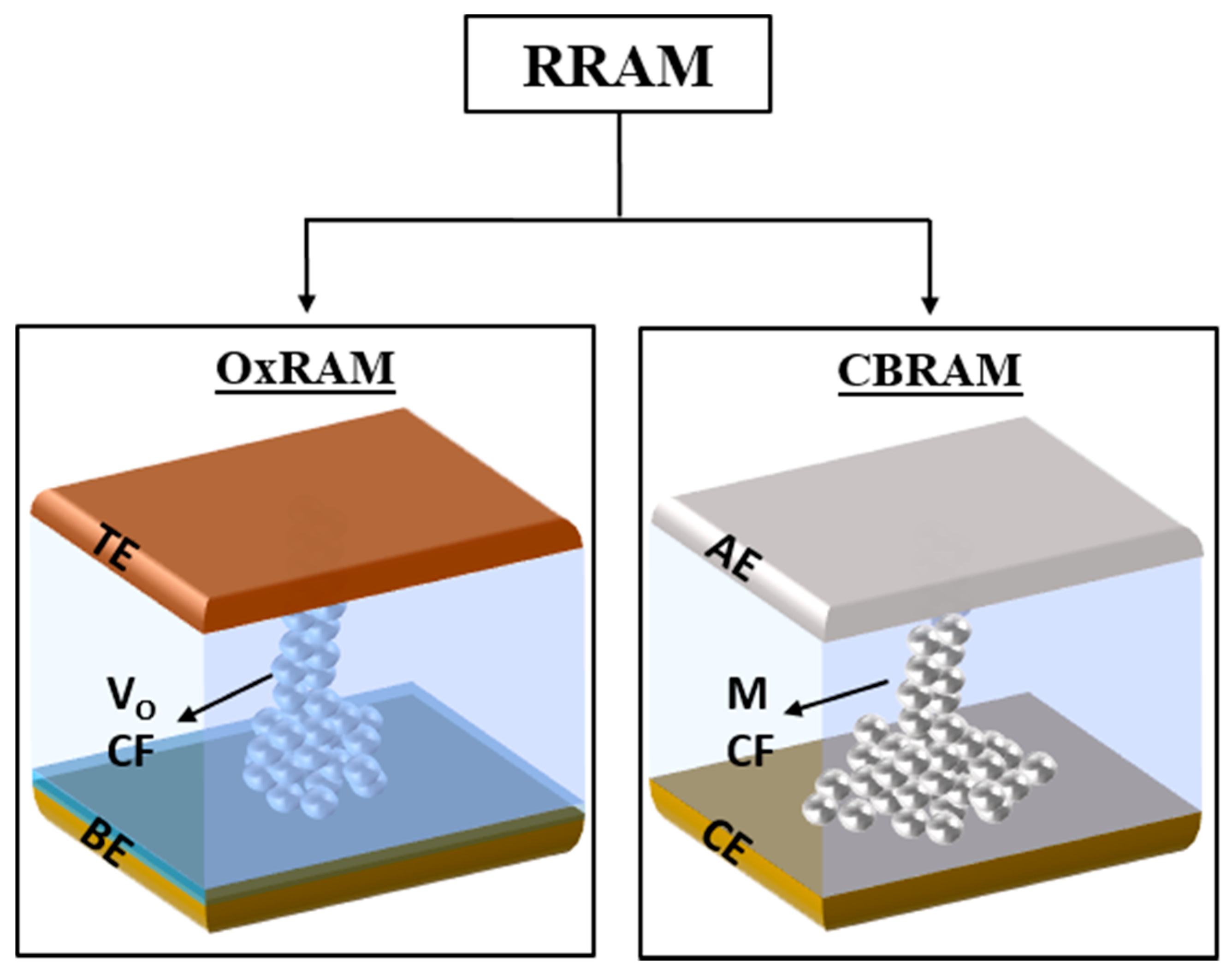
:1. Introduction
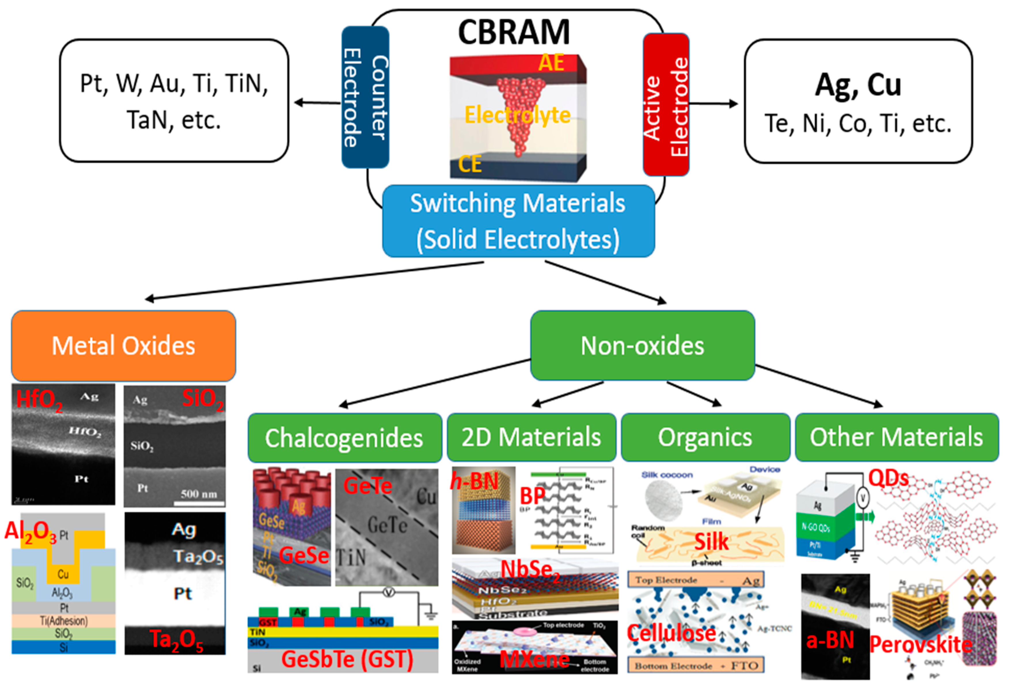
2. Electrode and Switching Materials
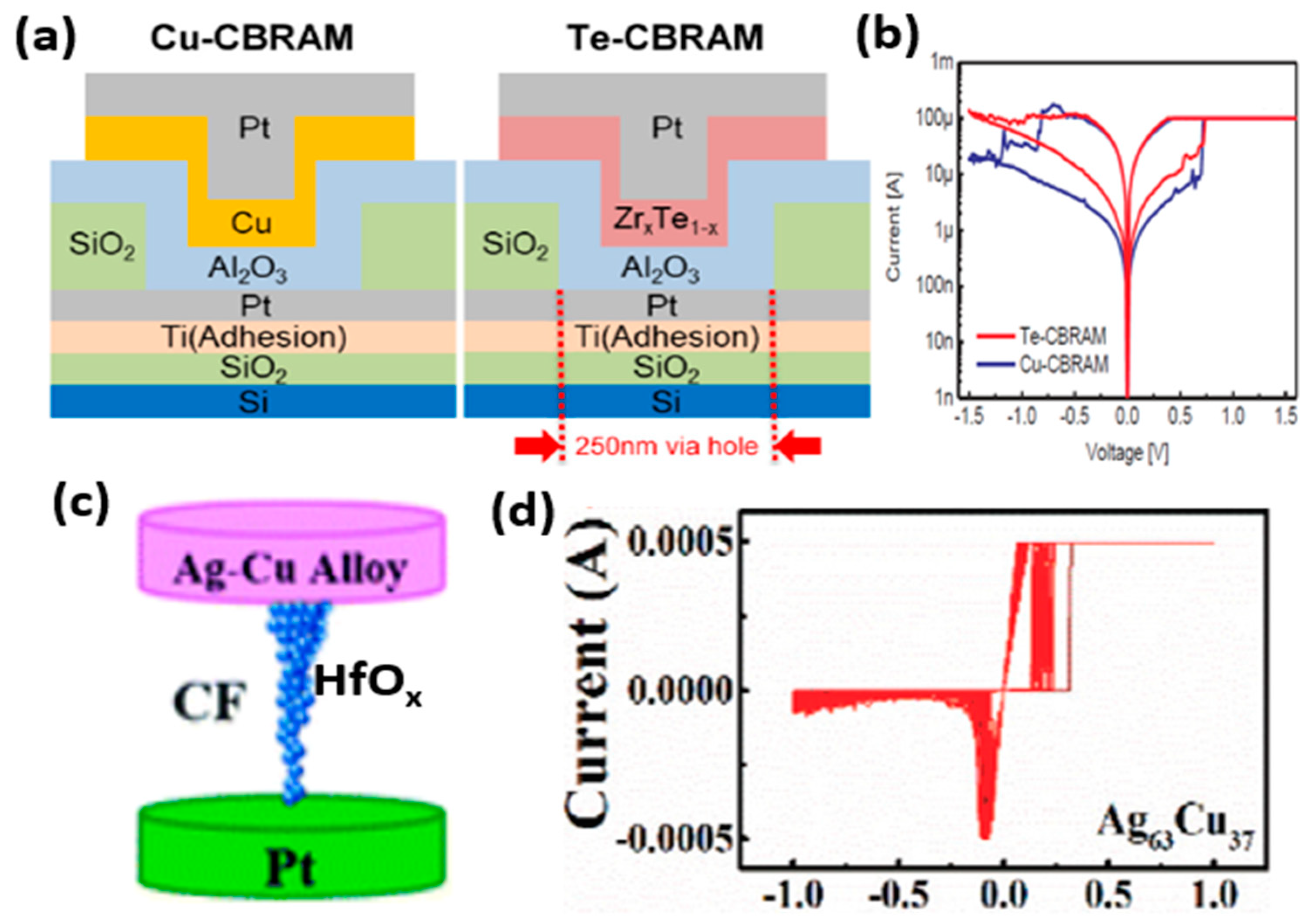
2.1. Electrode Materials
2.2. Switching Materials
2.2.1. Metal Oxides
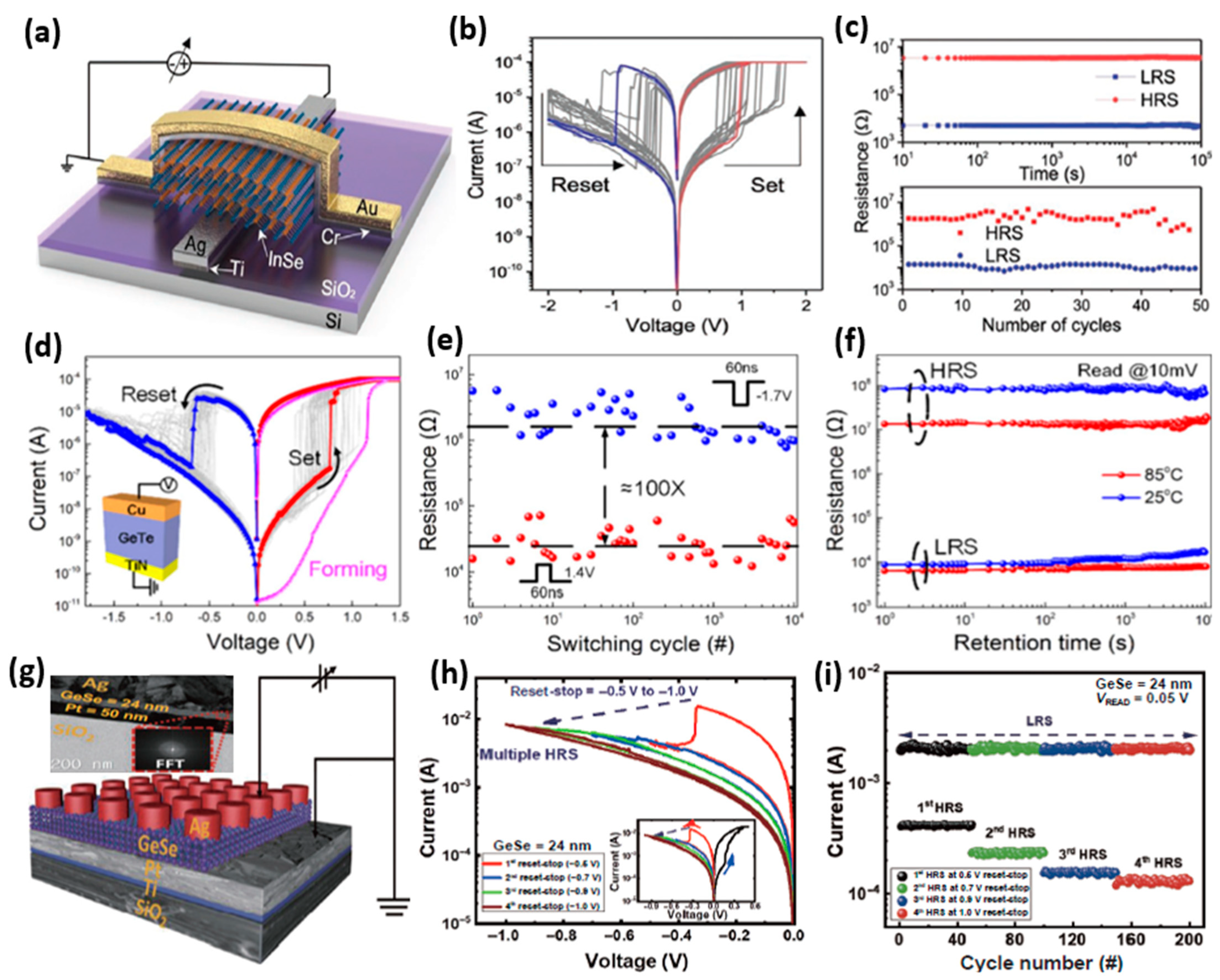
2.2.2. Non-Oxides
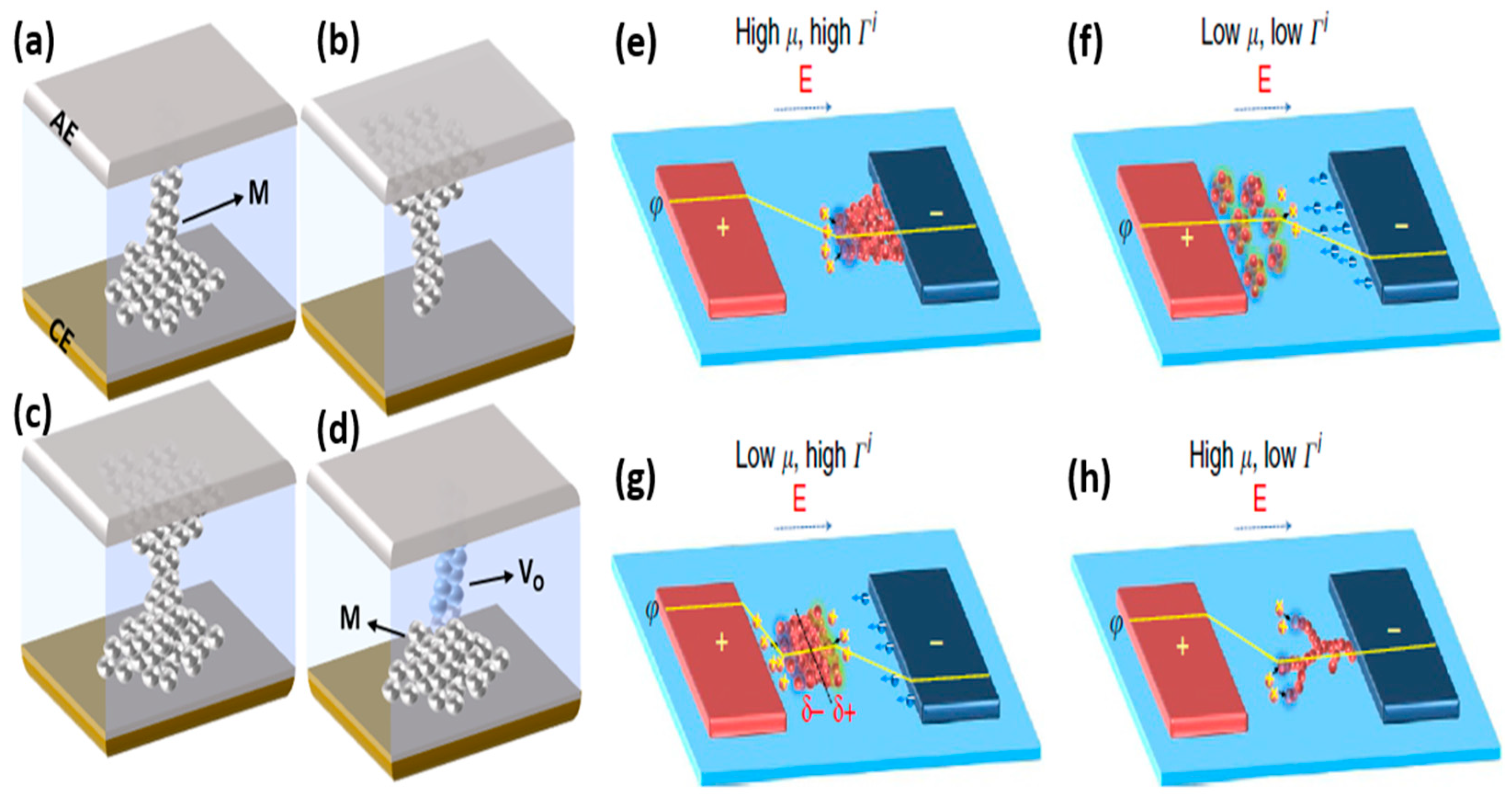
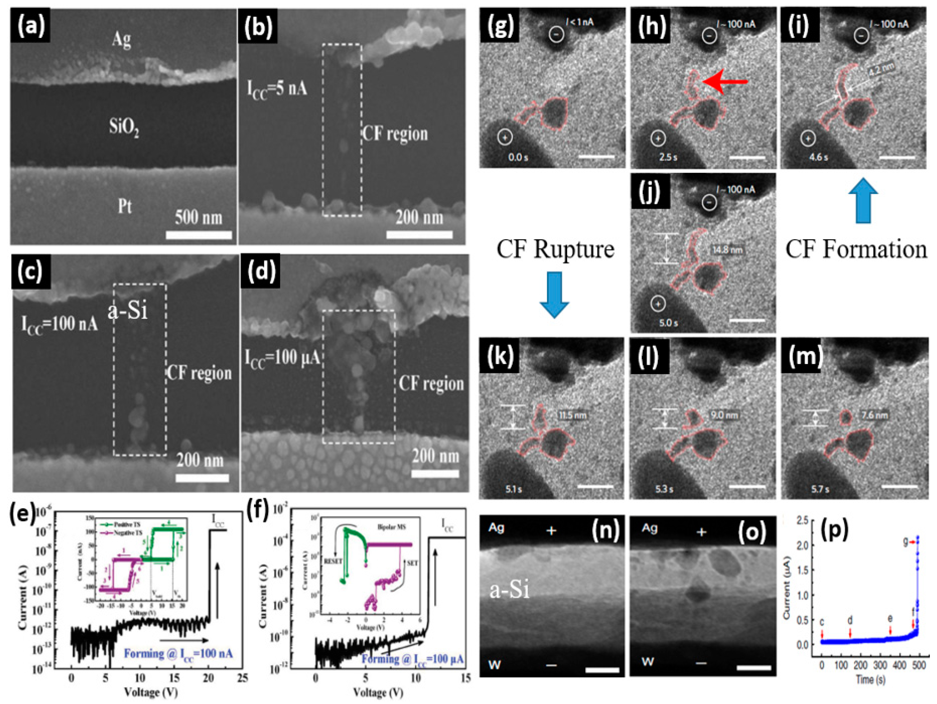
3. Switching Mechanisms
4. Memory Applications
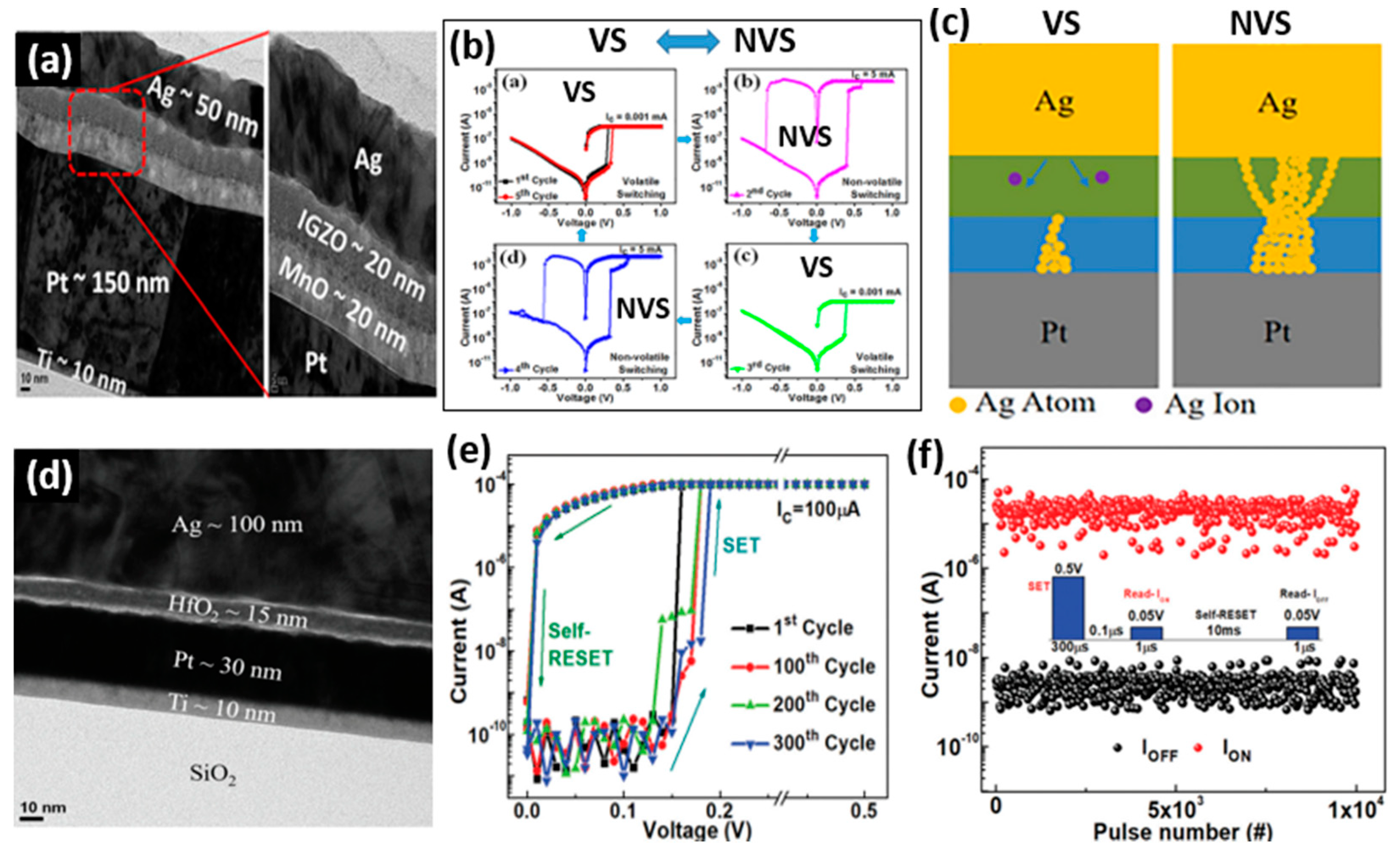
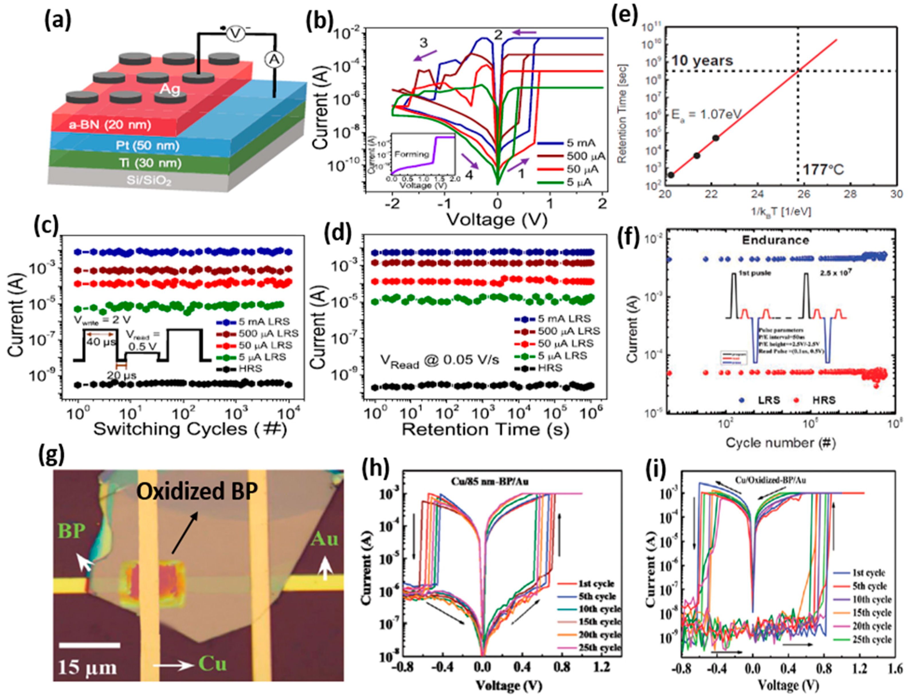
4.1. Volatile Memory
4.2. Nonvolatile Memory
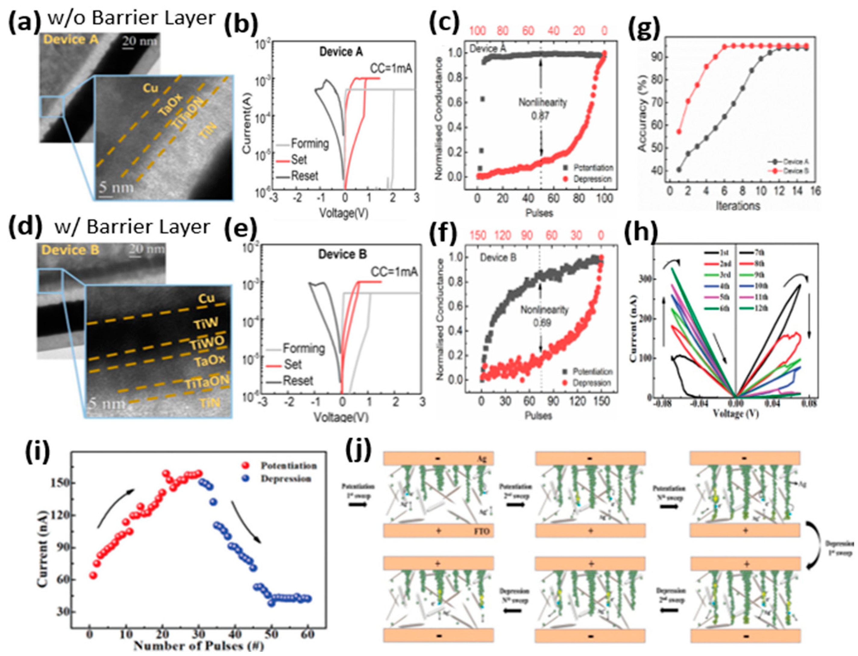
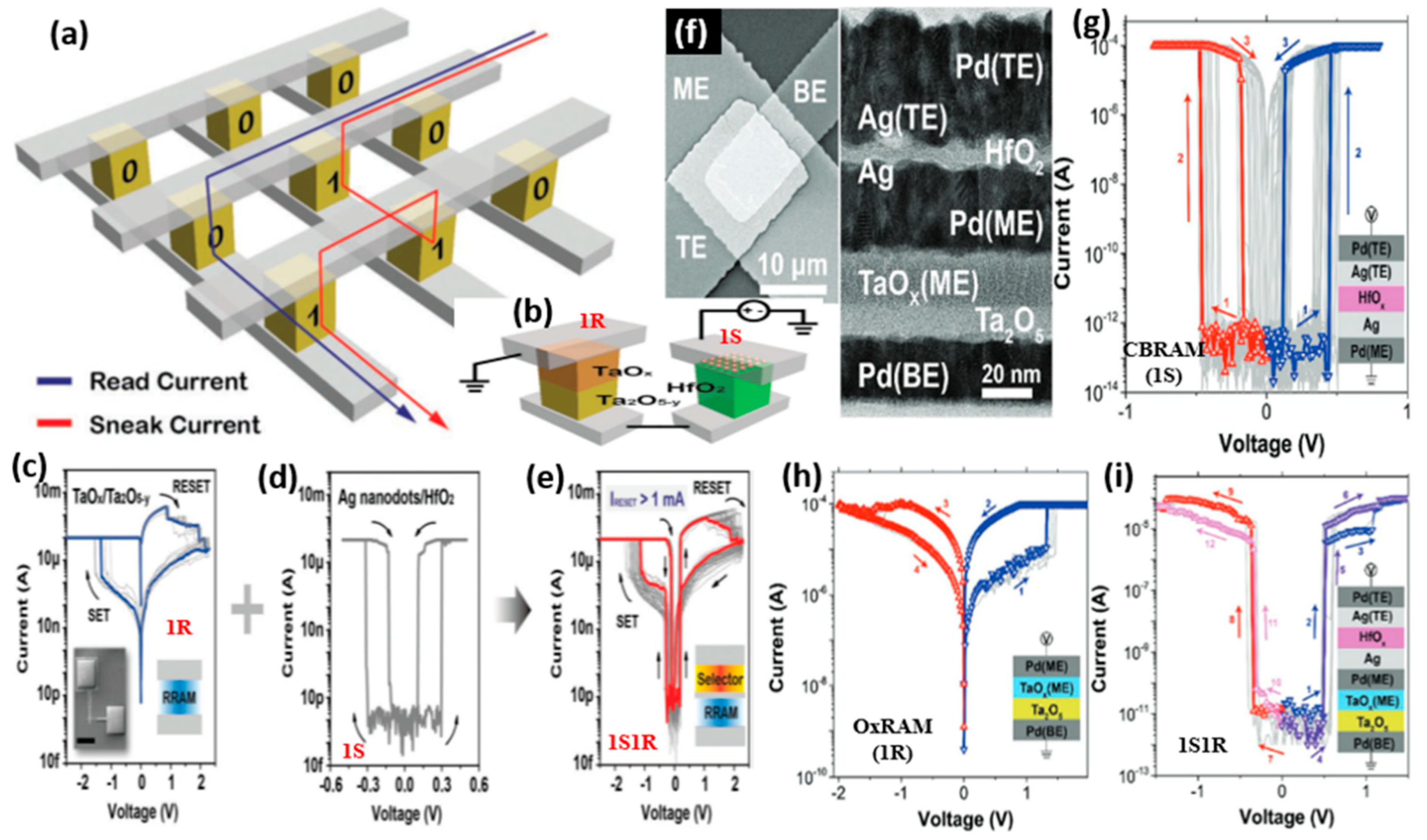
4.3. Selector for Memory
5. Neuromorphic Computing Applications
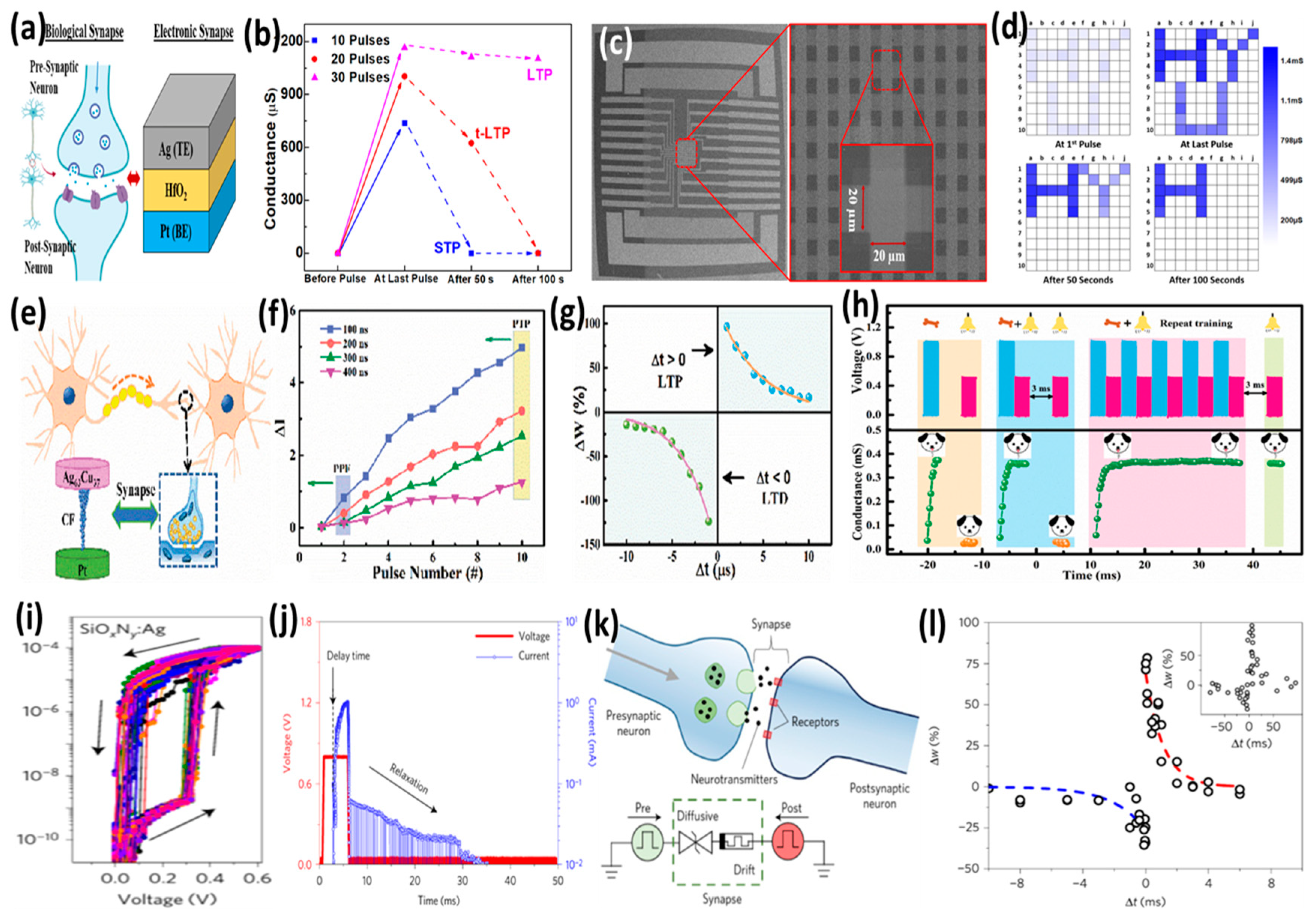
5.1. Emulation of Biological Synapses
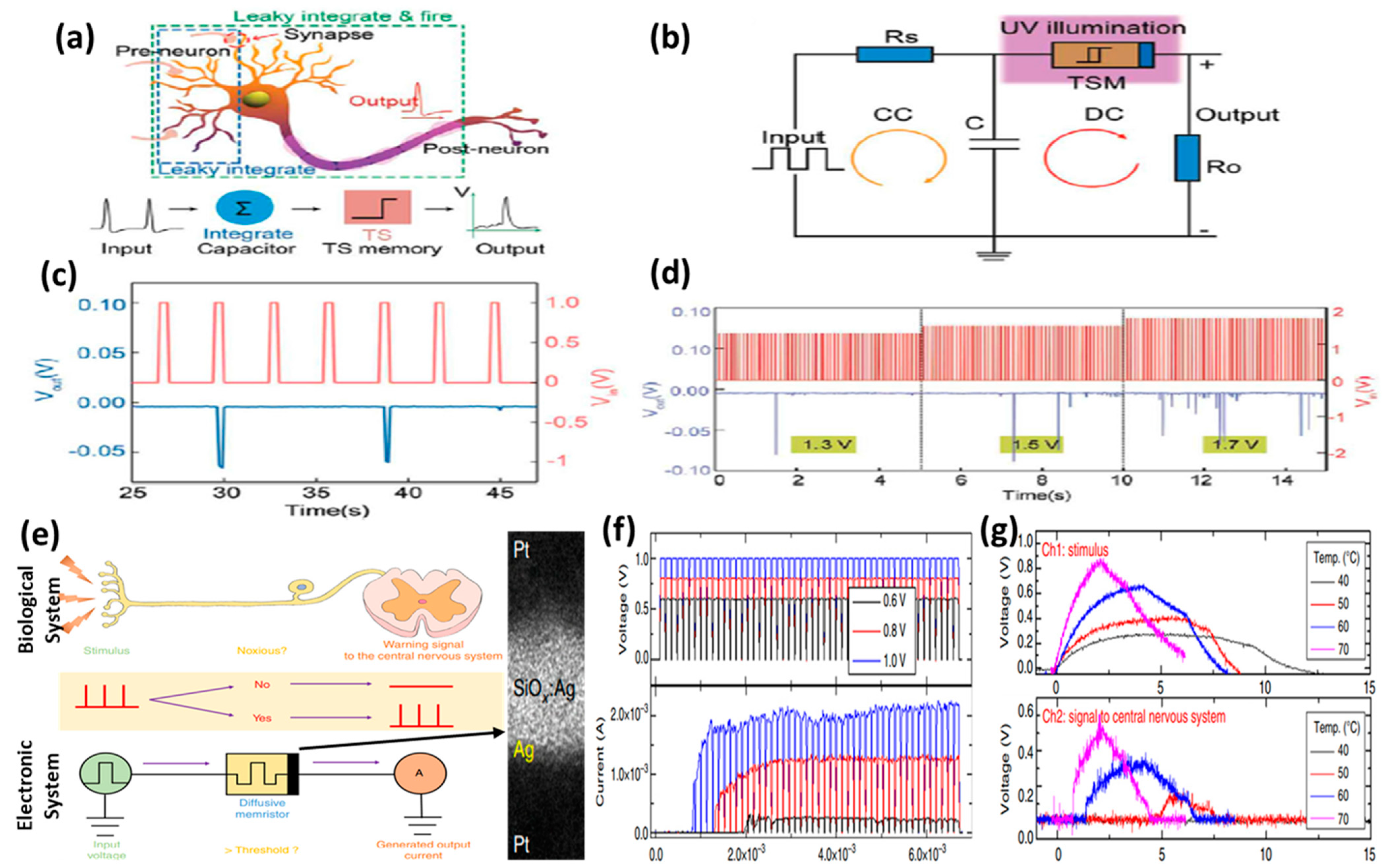
5.2. Emulation of Biological Neurons
6. Summary and Outlook
Author Contributions
Funding
Data Availability Statement
Conflicts of Interest
References
- Meena, J.S.; Sze, S.M.; Chand, U.; Tseng, T.Y. Overview of Emerging Nonvolatile Memory Technologies. Nanoscale Res. Lett. 2014, 9, 526. [Google Scholar] [CrossRef] [PubMed] [Green Version]
- Jeong, D.S.; Thomas, R.; Katiyar, R.S.; Scott, J.F.; Kohlstedt, H.; Petraru, A.; Hwang, C.S. Emerging Memories: Resistive Switching Mechanisms and Current Status. Rep. Prog. Phys. 2012, 75, 076502. [Google Scholar] [CrossRef]
- Sokolov, A.S.; Abbas, H.; Abbas, Y.; Choi, C. Towards Engineering in Memristors for Emerging Memory and Neuromorphic Computing: A Review. J. Semicond. 2021, 42, 013101. [Google Scholar] [CrossRef]
- Chen, A. A Review of Emerging Non-Volatile Memory (NVM) Technologies and Applications. Solid-State Electron. 2016, 125, 25–38. [Google Scholar] [CrossRef]
- Park, S.; Noh, J.; Choo, M.-L.; Sheri, A.M.; Chang, M.; Kim, Y.-B.; Kim, C.J.; Jeon, M.; Lee, B.-G.; Lee, B.H.; et al. Nanoscale RRAM-Based Synaptic Electronics: Toward a Neuromorphic Computing Device. Nanotechnology 2013, 24, 384009. [Google Scholar] [CrossRef]
- Li, Y.; Wang, Z.; Midya, R.; Xia, Q.; Yang, J.J. Review of Memristor Devices in Neuromorphic Computing: Materials Sciences and Device Challenges. J. Phys. D Appl. Phys. 2018, 51, 50. [Google Scholar] [CrossRef]
- Abbas, H.; Park, M.R.; Abbas, Y.; Hu, Q.; Kang, T.S.; Yoon, T.-S.; Kang, C.J. Resistive Switching Characteristics of Manganese Oxide Thin Film and Nanoparticle Assembly Hybrid Devices. Jpn. J. Appl. Phys. 2018, 57, 06HC03. [Google Scholar] [CrossRef]
- Abbas, H.; Abbas, Y.; Park, M.R.; Hu, Q.; Lee, T.S.; Cho, J.; Yoon, T.-S.; Choi, Y.J.; Kang, C.J. Resistive Switching Characteristics of Tantalum Oxide and Titanium Oxide Heterojunction Devices. J. Nanosci. Nanotechnol. 2017, 17, 7150–7154. [Google Scholar] [CrossRef]
- Prakash, A.; Hwang, H. Multilevel Cell Storage and Resistance Variability in Resistive Random Access Memory. Phys. Sci. Rev. 2016, 1, 20160010. [Google Scholar]
- Banerjee, W.; Hwang, H. Quantized Conduction Device with 6-Bit Storage Based on Electrically Controllable Break Junctions. Adv. Electron. Mater. 2019, 5, 1900744. [Google Scholar] [CrossRef]
- Wu, M.C.; Ting, Y.H.; Chen, J.Y.; Wu, W.W. Low Power Consumption Nanofilamentary ECM and VCM Cells in a Single Sidewall of High-Density VRRAM Arrays. Adv. Sci. 2019, 6, 1902363. [Google Scholar] [CrossRef] [PubMed]
- Lim, E.; Ismail, R. Conduction Mechanism of Valence Change Resistive Switching Memory: A Survey. Electronics 2015, 4, 586–613. [Google Scholar] [CrossRef]
- Adesto Technologies Acquires Atmel’s Serial Flash Product Families. Available online: https://www.Businesswire.Com/news/home/20121001005462/en/%20Adesto-Technologies-Acquires-Atmel%E2%80%99s-Serial-Flash-Product (accessed on 31 March 2022).
- Breakthrough Resistive RAM (ReRAM) Technology. Available online: https://www.Dialog-Semiconductor.Com/Products/Memory/Cbram-Technology (accessed on 31 March 2022).
- Zhou, G.; Wang, Z.; Sun, B.; Zhou, F.; Sun, L.; Zhao, H.; Hu, X.; Peng, X.; Yan, J.; Wang, H.; et al. Volatile and Nonvolatile Memristive Devices for Neuromorphic Computing. Adv. Electron. Mater. 2022, 2101127. [Google Scholar] [CrossRef]
- Wang, R.; Yang, J.-Q.; Mao, J.-Y.; Wang, Z.-P.; Wu, S.; Zhou, M.; Chen, T.; Zhou, Y.; Han, S.-T. Recent Advances of Volatile Memristors: Devices, Mechanisms, and Applications. Adv. Intell. Syst. 2020, 2, 2000055. [Google Scholar] [CrossRef]
- Abbas, H.; Abbas, Y.; Hassan, G.; Sokolov, A.S.; Jeon, Y.R.; Ku, B.; Kang, C.J.; Choi, C. The Coexistence of Threshold and Memory Switching Characteristics of ALD HfO2memristor Synaptic Arrays for Energy-Efficient Neuromorphic Computing. Nanoscale 2020, 12, 14120–14134. [Google Scholar] [CrossRef]
- Lee, T.S.; Lee, N.J.; Abbas, H.; Lee, H.H.; Yoon, T.-S.; Kang, C.J. Compliance Current-Controlled Conducting Filament Formation in Tantalum Oxide-Based RRAM Devices with Different Top Electrodes. ACS Appl. Electron. Mater. 2020, 2, 1154–1161. [Google Scholar] [CrossRef]
- Lee, S.; Song, J.; Lim, S.; Chekol, S.A.; Hwang, H. Excellent Data Retention Characteristic of Te-Based Conductive-Bridge RAM Using Semiconducting Te Filament for Storage Class Memory. Solid-State Electron. 2019, 153, 8–11. [Google Scholar] [CrossRef]
- Sun, H.; Liu, Q.; Li, C.; Long, S.; Lv, H.; Bi, C.; Huo, Z.; Li, L.; Liu, M. Direct Observation of Conversion Between Threshold Switching and Memory Switching Induced by Conductive Filament Morphology. Adv. Funct. Mater. 2014, 24, 5679–5686. [Google Scholar] [CrossRef]
- Jin, M.-M.; Cheng, L.; Li, Y.; Hu, S.-Y.; Lu, K.; Chen, J.; Duan, N.; Wang, Z.-R.; Zhou, Y.-X.; Chang, T.-C.; et al. Reconfigurable Logic in Nanosecond Cu/GeTe/TiN Filamentary Memristors for Energy-Efficient in-Memory Computing. Nanotechnology 2018, 29, 385203. [Google Scholar] [CrossRef]
- Rebora, C.; Huang, R.; Kissling, G.P.; Bocquet, M.; de Groot, K.; Favre, L.; Grosso, D.; Deleruyelle, D.; Putero, M. Conductive-Bridge Memory Cells Based on a Nanoporous Electrodeposited GeSbTe Alloy. Nanotechnology 2019, 30, 025202. [Google Scholar] [CrossRef]
- Ali, A.; Abbas, H.; Hussain, M.; Jaffery, S.H.A.; Hussain, S.; Choi, C.; Jung, J. Thickness-Dependent Monochalcogenide GeSe-Based CBRAM for Memory and Artificial Electronic Synapses. Nano Res. 2022, 15, 2263–2277. [Google Scholar] [CrossRef]
- Pan, C.; Ji, Y.; Xiao, N.; Hui, F.; Tang, K.; Guo, Y.; Xie, X.; Puglisi, F.M.; Larcher, L.; Miranda, E.; et al. Coexistence of Grain-Boundaries-Assisted Bipolar and Threshold Resistive Switching in Multilayer Hexagonal Boron Nitride. Adv. Funct. Mater. 2017, 27, 1604811. [Google Scholar] [CrossRef]
- Rehman, S.; Khan, M.F.; Aftab, S.; Kim, H.; Eom, J.; Kim, D. Thickness-Dependent Resistive Switching in Black Phosphorus CBRAM. J. Mater. Chem. C 2019, 7, 725–732. [Google Scholar] [CrossRef]
- Sokolov, A.; Ali, M.; Li, H.; Jeon, Y.; Ko, M.J.; Choi, C. Partially Oxidized MXene Ti3C2Tx Sheets for Memristor Having Synapse and Threshold Resistive Switching Characteristics. Adv. Electron. Mater. 2021, 7, 2000866. [Google Scholar] [CrossRef]
- Jeon, Y.-R.; Choi, J.; Kwon, J.-D.; Park, M.H.; Kim, Y.; Choi, C. Suppressed Stochastic Switching Behavior and Improved Synaptic Functions in an Atomic Switch Embedded with a 2D NbSe2 Material. ACS Appl. Mater. Interfaces 2021, 13, 10161–10170. [Google Scholar] [CrossRef] [PubMed]
- Zhao, M.; Wang, S.; Li, D.; Wang, R.; Li, F.; Wu, M.; Liang, K.; Ren, H.; Zheng, X.; Guo, C.; et al. Silk Protein Based Volatile Threshold Switching Memristors for Neuromorphic Computing. Adv. Electron. Mater. 2022, 8, 2101139. [Google Scholar] [CrossRef]
- Hussain, T.; Abbas, H.; Youn, C.; Lee, H.; Boynazarov, T.; Ku, B.; Jeon, Y.; Han, H.; Lee, J.H.; Choi, C.; et al. Cellulose Nanocrystal Based Bio-Memristor as a Green Artificial Synaptic Device for Neuromorphic Computing Applications. Adv. Mater. Technol. 2022, 7, 2100744. [Google Scholar] [CrossRef]
- Sokolov, A.S.; Ali, M.; Riaz, R.; Abbas, Y.; Ko, M.J.; Choi, C. Silver-Adapted Diffusive Memristor Based on Organic Nitrogen-Doped Graphene Oxide Quantum Dots (N-GOQDs) for Artificial Biosynapse Applications. Adv. Funct. Mater. 2019, 29, 1807504. [Google Scholar] [CrossRef]
- Jeon, Y.R.; Abbas, Y.; Sokolov, A.S.; Kim, S.; Ku, B.; Choi, C. Study of in Situ Silver Migration in Amorphous Boron Nitride CBRAM Device. ACS Appl. Mater. Interfaces 2019, 11, 23329–23336. [Google Scholar] [CrossRef]
- Ku, B.; Koo, B.; Sokolov, A.S.; Ko, M.J.; Choi, C. Two-Terminal Artificial Synapse with Hybrid Organic–Inorganic Perovskite (CH3NH3)PbI3 and Low Operating Power Energy (~47 FJ/Μm2). J. Alloy. Compd. 2020, 833, 155064. [Google Scholar] [CrossRef]
- Chekol, S.A.; Menzel, S.; Ahmad, R.W.; Waser, R.; Hoffmann-Eifert, S. Effect of the Threshold Kinetics on the Filament Relaxation Behavior of Ag-Based Diffusive Memristors. Adv. Funct. Mater. 2021, 32, 2111242. [Google Scholar] [CrossRef]
- Yang, Y.; Gao, P.; Li, L.; Pan, X.; Tappertzhofen, S.; Choi, S.; Waser, R.; Valov, I.; Lu, W.D. Electrochemical Dynamics of Nanoscale Metallic Inclusions in Dielectrics. Nat. Commun. 2014, 5, 4232. [Google Scholar] [CrossRef] [PubMed] [Green Version]
- Hsu, C.-L.; Saleem, A.; Singh, A.; Kumar, D.; Tseng, T.-Y. Enhanced Linearity in CBRAM Synapse by Post Oxide Deposition Annealing for Neuromorphic Computing Applications. IEEE Trans. Electron Devices 2021, 68, 5578–5584. [Google Scholar] [CrossRef]
- Belmonte, A.; Witters, T.; Covello, A.; Vereecke, G.; Franquet, A.; Spampinato, V.; Kundu, S.; Mao, M.; Hody, H.; Kar, G.S.; et al. Co Active Electrode Enhances CBRAM Performance and Scaling Potential. In Proceedings of the 2019 IEEE International Electron Devices Meeting (IEDM), San Francisco, CA, USA, 7–11 December 2019; pp. 35.8.1–35.8.4. [Google Scholar]
- Sonde, S.; Chakrabarti, B.; Liu, Y.; Sasikumar, K.; Lin, J.; Stan, L.; Divan, R.; Ocola, L.E.; Rosenmann, D.; Choudhury, P.; et al. Silicon Compatible Sn-Based Resistive Switching Memory. Nanoscale 2018, 10, 9441–9449. [Google Scholar] [CrossRef] [PubMed]
- Choi, Y.-J.; Bang, S.; Kim, T.-H.; Lee, D.K.; Hong, K.; Kim, S.; Park, B.-G. Effect of Ag Source Layer Thickness on the Switching Mechanism of TiN/Ag/SiNx/TiN Conductive Bridging Random Access Memory Observed at Sub-ΜA Current. Semicond. Sci. Technol. 2021, 36, 055014. [Google Scholar] [CrossRef]
- Kumar, D.; Aluguri, R.; Chand, U.; Tseng, T.-Y. Conductive Bridge Random Access Memory Characteristics of SiCN Based Transparent Device Due to Indium Diffusion. Nanotechnology 2018, 29, 125202. [Google Scholar] [CrossRef]
- Wang, J.; Cao, G.; Sun, K.; Lan, J.; Pei, Y.; Chen, J.; Yan, X. Alloy Electrode Engineering in Memristors for Emulating the Biological Synapse. Nanoscale 2022, 14, 1318–1326. [Google Scholar] [CrossRef]
- Ismail, M.; Abbas, H.; Choi, C.; Kim, S. Controllable Analog Resistive Switching and Synaptic Characteristics in ZrO2/ZTO Bilayer Memristive Device for Neuromorphic Systems. Appl. Surf. Sci. 2020, 529, 147107. [Google Scholar] [CrossRef]
- Abbas, H.; Abbas, Y.; Truong, S.N.; Min, K.S.; Park, M.R.; Cho, J.; Yoon, T.S.; Kang, C.J. A Memristor Crossbar Array of Titanium Oxide for Non-Volatile Memory and Neuromorphic Applications. Semicond. Sci. Technol. 2017, 32, 065014. [Google Scholar] [CrossRef]
- Yu, J.; Xu, X.; Gong, T.; Luo, Q.; Dong, D.; Yuan, P.; Tai, L.; Yin, J.; Zhu, X.; Wu, X.; et al. Suppression of Filament Overgrowth in Conductive Bridge Random Access Memory by Ta2O5/TaOx Bi-Layer Structure. Nanoscale Res. Lett. 2019, 14, 111. [Google Scholar] [CrossRef] [Green Version]
- Li, D.; Ilyas, N.; Li, C.; Jiang, X.; Jiang, Y.; Li, W. Synaptic Learning and Memory Functions in SiO2:Ag/TiO2 Based Memristor Devices. J. Phys. D Appl. Phys. 2020, 53, 175102. [Google Scholar] [CrossRef]
- Ali, A.; Abbas, Y.; Abbas, H.; Jeon, Y.R.; Hussain, S.; Naqvi, B.A.; Choi, C.; Jung, J. Dependence of InGaZnO and SnO2 Thin Film Stacking Sequence for the Resistive Switching Characteristics of Conductive Bridge Memory Devices. Appl. Surf. Sci. 2020, 525, 146390. [Google Scholar] [CrossRef]
- Huh, W.; Lee, D.; Lee, C. Memristors Based on 2D Materials as an Artificial Synapse for Neuromorphic Electronics. Adv. Mater. 2020, 32, 2002092. [Google Scholar] [CrossRef]
- Chen, S.; Mahmoodi, M.R.; Shi, Y.; Mahata, C.; Yuan, B.; Liang, X.; Wen, C.; Hui, F.; Akinwande, D.; Strukov, D.B.; et al. Wafer-Scale Integration of Two-Dimensional Materials in High-Density Memristive Crossbar Arrays for Artificial Neural Networks. Nat. Electron. 2020, 3, 638–645. [Google Scholar] [CrossRef]
- Dastgeer, G.; Abbas, H.; Kim, D.Y.; Eom, J.; Choi, C. Synaptic Characteristics of an Ultrathin Hexagonal Boron Nitride (h-BN) Diffusive Memristor. Phys. Status Solidi (RRL)—Rapid Res. Lett. 2021, 15, 2000473. [Google Scholar] [CrossRef]
- Zhang, J.; Huang, J. Neuromorphic Devices Based on Organic Materials. In Neuromorphic Devices for Brain-Inspired Computing; Wiley: Hoboken, NJ, USA, 2022; pp. 149–172. [Google Scholar]
- Mazumder, A.; Ahmed, T.; Mayes, E.; Tawfik, S.A.; Russo, S.P.; Low, M.X.; Ranjan, A.; Balendhran, S.; Walia, S. Nonvolatile Resistive Switching in Layered InSe via Electrochemical Cation Diffusion. Adv. Electron. Mater. 2022, 8, 2100999. [Google Scholar] [CrossRef]
- Wang, Z.; Joshi, S.; Savel’ev, S.E.; Jiang, H.; Midya, R.; Lin, P.; Hu, M.; Ge, N.; Strachan, J.P.; Li, Z.; et al. Memristors with Diffusive Dynamics as Synaptic Emulators for Neuromorphic Computing. Nat. Mater. 2017, 16, 101–108. [Google Scholar] [CrossRef] [PubMed] [Green Version]
- Yang, Y.; Gao, P.; Gaba, S.; Chang, T.; Pan, X.; Lu, W. Observation of Conducting Filament Growth in Nanoscale Resistive Memories. Nat. Commun. 2012, 3, 732. [Google Scholar] [CrossRef]
- Banerjee, W.; Karpov, I.v.; Agrawal, A.; Kim, S.; Lee, S.; Lee, S.; Lee, D.; Hwang, H. Highly-Stable (<3% Fluctuation) Ag-Based Threshold Switch with Extreme-Low OFF Current of 0.1 PA, Extreme-High Selectivity of 109 and High Endurance of 109 Cycles. In Proceedings of the 2020 IEEE International Electron Devices Meeting (IEDM), San Francisco, CA, USA, 12–18 December 2020; pp. 28.4.1–28.4.4. [Google Scholar]
- Wu, F.; Si, S.; Cao, P.; Wei, W.; Zhao, X.; Shi, T.; Zhang, X.; Ma, J.; Cao, R.; Liao, L.; et al. Interface Engineering via MoS2 Insertion Layer for Improving Resistive Switching of Conductive-Bridging Random Access Memory. Adv. Electron. Mater. 2019, 5, 1800747. [Google Scholar] [CrossRef]
- Li, Y.; Yin, L.; Wu, Z.; Li, X.; Song, X.; Gao, X.; Fu, L. Improved Resistive Switching Uniformity of SiO2 Electrolyte-Based Resistive Random Access Memory Device With Cu Oxidizable Electrode. IEEE Electron Device Lett. 2019, 40, 1599–1601. [Google Scholar] [CrossRef]
- Song, J.; Woo, J.; Lim, S.; Chekol, S.A.; Hwang, H. Self-Limited CBRAM With Threshold Selector for 1S1R Crossbar Array Applications. IEEE Electron Device Lett. 2017, 38, 1532–1535. [Google Scholar] [CrossRef]
- Abbas, H.; Ali, A.; Jung, J.; Hu, Q.; Park, M.R.; Lee, H.H.; Yoon, T.-S.; Kang, C.J. Reversible Transition of Volatile to Non-Volatile Resistive Switching and Compliance Current-Dependent Multistate Switching in IGZO/MnO RRAM Devices. Appl. Phys. Lett. 2019, 114, 093503. [Google Scholar] [CrossRef]
- Khot, A.C.; Dongale, T.D.; Nirmal, K.A.; Sung, J.H.; Lee, H.J.; Nikam, R.D.; Kim, T.G. Amorphous Boron Nitride Memristive Device for High-Density Memory and Neuromorphic Computing Applications. ACS Appl. Mater. Interfaces 2022, 14, 10546–10557. [Google Scholar] [CrossRef]
- Choi, S.H.; Park, S.O.; Seo, S.; Choi, S. Reliable Multilevel Memristive Neuromorphic Devices Based on Amorphous Matrix via Quasi-1D Filament Confinement and Buffer Layer. Sci. Adv. 2022, 8, 7866. [Google Scholar] [CrossRef] [PubMed]
- Kim, H.J.; Kim, J.; Park, T.G.; Yoon, J.H.; Hwang, C.S. Multi-Level Control of Conductive Filament Evolution and Enhanced Resistance Controllability of the Cu-Cone Structure Embedded Conductive Bridge Random Access Memory. Adv. Electron. Mater. 2021, 2100209. [Google Scholar] [CrossRef]
- Abbas, Y.; Ambade, R.B.; Ambade, S.B.; Han, T.H.; Choi, C. Tailored Nanoplateau and Nanochannel Structures Using Solution-Processed Rutile TiO2 Thin Films for Complementary and Bipolar Switching Characteristics. Nanoscale 2019, 11, 13815–13823. [Google Scholar] [CrossRef]
- Pi, S.; Li, C.; Jiang, H.; Xia, W.; Xin, H.; Yang, J.J.; Xia, Q. Memristor Crossbar Arrays with 6-Nm Half-Pitch and 2-Nm Critical Dimension. Nat. Nanotechnol. 2019, 14, 35–39. [Google Scholar] [CrossRef]
- Xia, Q.; Yang, J.J. Memristive Crossbar Arrays for Brain-Inspired Computing. Nat. Mater. 2019, 18, 309–323. [Google Scholar] [CrossRef]
- Yoon, J.H.; Song, S.J.; Yoo, I.-H.; Seok, J.Y.; Yoon, K.J.; Kwon, D.E.; Park, T.H.; Hwang, C.S. Highly Uniform, Electroforming-Free, and Self-Rectifying Resistive Memory in the Pt/Ta2O5/HfO2-x/TiN Structure. Adv. Funct. Mater. 2014, 24, 5086–5095. [Google Scholar] [CrossRef]
- Gao, S.; Zeng, F.; Li, F.; Wang, M.; Mao, H.; Wang, G.; Song, C.; Pan, F. Forming-Free and Self-Rectifying Resistive Switching of the Simple Pt/TaO x /n-Si Structure for Access Device-Free High-Density Memory Application. Nanoscale 2015, 7, 6031–6038. [Google Scholar] [CrossRef]
- Ismail, M.; Mahata, C.; Abbas, H.; Choi, C.; Kim, S. Bipolar, Complementary Resistive Switching and Synaptic Properties of Sputtering Deposited ZnSnO-Based Devices for Electronic Synapses. J. Alloys Compd. 2021, 862, 158416. [Google Scholar] [CrossRef]
- Rao, M.; Song, W.; Kiani, F.; Asapu, S.; Zhuo, Y.; Midya, R.; Upadhyay, N.; Wu, Q.; Barnell, M.; Lin, P.; et al. Timing Selector: Using Transient Switching Dynamics to Solve the Sneak Path Issue of Crossbar Arrays. Small Sci. 2022, 2, 2100072. [Google Scholar] [CrossRef]
- Song, J.; Prakash, A.; Lee, D.; Woo, J.; Cha, E.; Lee, S.; Hwang, H. Bidirectional Threshold Switching in Engineered Multilayer (Cu2O/Ag:Cu2O/Cu2O) Stack for Cross-Point Selector Application. Appl. Phys. Lett. 2015, 107, 113504. [Google Scholar] [CrossRef]
- Hua, Q.; Wu, H.; Gao, B.; Zhao, M.; Li, Y.; Li, X.; Hou, X.; (Marvin) Chang, M.-F.; Zhou, P.; Qian, H. A Threshold Switching Selector Based on Highly Ordered Ag Nanodots for X-Point Memory Applications. Adv. Sci. 2019, 6, 1900024. [Google Scholar] [CrossRef] [PubMed]
- Midya, R.; Wang, Z.; Zhang, J.; Savel’ev, S.E.; Li, C.; Rao, M.; Jang, M.H.; Joshi, S.; Jiang, H.; Lin, P.; et al. Anatomy of Ag/Hafnia-Based Selectors with 1010 Nonlinearity. Adv. Mater. 2017, 29, 1604457. [Google Scholar] [CrossRef] [PubMed] [Green Version]
- Song, J.; Woo, J.; Prakash, A.; Lee, D.; Hwang, H. Threshold Selector with High Selectivity and Steep Slope for Cross-Point Memory Array. IEEE Electron Device Lett. 2015, 36, 681–683. [Google Scholar] [CrossRef]
- Cha, J.-H.; Yang, S.Y.; Oh, J.; Choi, S.; Park, S.; Jang, B.C.; Ahn, W.; Choi, S.-Y. Conductive-Bridging Random-Access Memories for Emerging Neuromorphic Computing. Nanoscale 2020, 12, 14339–14368. [Google Scholar] [CrossRef]
- Tang, Y.P.; Shimizu, E.; Dube, G.R.; Rampon, C.; Kerchner, G.A.; Zhuo, M.; Liu, G.; Tsien, J.Z. Genetic Enhancement of Learning and Memory in Mice. Nature 1999, 401, 63–69. [Google Scholar] [CrossRef]
- Bliss, T.V.P.; Collingridge, G.L. A Synaptic Model of Memory: Long-Term Potentiation in the Hippocampus. Nature 1993, 361, 31–39. [Google Scholar] [CrossRef]
- Atkinson, R.C.; Shiffrin, R.M. Human Memory: A Proposed System and Its Control Processes. In Psychology of Learning and Motivation—Advances in Research and Theory; Academic Press: New York, NY, USA, 1968; Volume 2, pp. 89–195. [Google Scholar]
- Pavlov, I.P. Conditioned Reflexes: An Investigation of the Physiological Activity of the Cerebral Cortex. Ann. Neurosci. 2010, 17, 136. [Google Scholar] [CrossRef] [Green Version]
- John, R.A.; Liu, F.; Chien, N.A.; Kulkarni, M.R.; Zhu, C.; Fu, Q.; Basu, A.; Liu, Z.; Mathews, N. Synergistic Gating of Electro-Iono-Photoactive 2D Chalcogenide Neuristors: Coexistence of Hebbian and Homeostatic Synaptic Metaplasticity. Adv. Mater. 2018, 30, 1800220. [Google Scholar] [CrossRef] [PubMed]
- Banerjee, W.; Nikam, R.D.; Hwang, H. Prospect and Challenges of Analog Switching for Neuromorphic Hardware. Appl. Phys. Lett. 2022, 120, 060501. [Google Scholar] [CrossRef]
- Ismail, M.; Abbas, H.; Sokolov, A.; Mahata, C.; Choi, C.; Kim, S. Emulating Synaptic Plasticity and Resistive Switching Characteristics through Amorphous Ta2O5 Embedded Layer for Neuromorphic Computing. Ceram. Int. 2021, 47, 30764–30776. [Google Scholar] [CrossRef]
- Saleem, A.; Simanjuntak, F.M.; Chandrasekaran, S.; Rajasekaran, S.; Tseng, T.-Y.; Prodromakis, T. Transformation of Digital to Analog Switching in TaOx-Based Memristor Device for Neuromorphic Applications. Appl. Phys. Lett. 2021, 118, 112103. [Google Scholar] [CrossRef]
- Tang, J.; Yuan, F.; Shen, X.; Wang, Z.; Rao, M.; He, Y.; Sun, Y.; Li, X.; Zhang, W.; Li, Y.; et al. Bridging Biological and Artificial Neural Networks with Emerging Neuromorphic Devices: Fundamentals, Progress, and Challenges. Adv. Mater. 2019, 31, 1902761. [Google Scholar] [CrossRef] [PubMed]
- Wang, J.; Lv, Z.; Xing, X.; Li, X.; Wang, Y.; Chen, M.; Pang, G.; Qian, F.; Zhou, Y.; Han, S. Optically Modulated Threshold Switching in Core–Shell Quantum Dot Based Memristive Device. Adv. Funct. Mater. 2020, 30, 1909114. [Google Scholar] [CrossRef]
- Zhang, Y.; He, W.; Wu, Y.; Huang, K.; Shen, Y.; Su, J.; Wang, Y.; Zhang, Z.; Ji, X.; Li, G.; et al. Highly Compact Artificial Memristive Neuron with Low Energy Consumption. Small 2018, 14, 1802188. [Google Scholar] [CrossRef]
- Yoon, J.H.; Wang, Z.; Kim, K.M.; Wu, H.; Ravichandran, V.; Xia, Q.; Hwang, C.S.; Yang, J.J. An Artificial Nociceptor Based on a Diffusive Memristor. Nat. Commun. 2018, 9, 417. [Google Scholar] [CrossRef]
- Jiang, H.; Belkin, D.; Savel’ev, S.E.; Lin, S.; Wang, Z.; Li, Y.; Joshi, S.; Midya, R.; Li, C.; Rao, M.; et al. A Novel True Random Number Generator Based on a Stochastic Diffusive Memristor. Nat. Commun. 2017, 8, 882. [Google Scholar] [CrossRef] [Green Version]
- Zhang, R.; Jiang, H.; Wang, Z.R.; Lin, P.; Zhuo, Y.; Holcomb, D.; Zhang, D.H.; Yang, J.J.; Xia, Q. Nanoscale Diffusive Memristor Crossbars as Physical Unclonable Functions. Nanoscale 2018, 10, 2721–2726. [Google Scholar] [CrossRef]


| Device Structure | VSET/VRESET (V) | ON/OFF Ratio | Endurance (Cycles) | Retention (s) | Refs. |
|---|---|---|---|---|---|
| Ag/HfO2/Pt | +0.19/−0.23 | 105 | 104 | 5 × 10⁴ | [17] |
| Ag/HfO2/Pt | +0.6/−0.5 | 109 | 108 | - | [53] |
| AgTe/HfO2/Pt | - | 109 | 109 | - | [53] |
| Ag/ZrO2/MoS2/Pt | +0.8/−0.2 | 106 | 102 | 104 | [54] |
| Ag/Ta2O5/Pt | +0.15/−0.5 | 104 | >450 | >104 | [18] |
| Cu/Al2O3/TiN | +2/−1 | 104 | - | - | [36] |
| Co/Al2O3/TiN | +2/−1 | 104 | 107 | 5 × 10⁴ | [36] |
| Co/LaSiO/TiN | +1.2/−0.5 | 600 | >103 | - | [36] |
| Sn/HfO2/Sn/Pt | +3/−2 | 104 | 225 | 105 | [37] |
| Cu/Ta2O5/TaOx/Ta/W | +2/−1 | 103 | >106 | >104 | [43] |
| Cu/SiO2/Pt | +0.75/−0.64 | ~10 | - | - | [55] |
| Ag/SiO2/Pt | +0.86/−0.67 | 104 | - | - | [55] |
| Te/MgO/HfOx/TiN | +0.7/−0.8 | ~10 | 104 | 104 | [35] |
| Cr-Au/InSe/Ag | +1/−1 | 102 | >50 | >105 | [50] |
| Ag/GeSe/Pt | +0.2/−0.2 | 103 | >106 | >105 | [23] |
| Cu/BP/Au | +0.6/−0.6 | 105 | 25 | 104 | [25] |
| Cu/GST/Pt | +0.5/−0.5 | 104 | - | 104 | [56] |
| Cu/GeTe/TiN | +0.75/−0.75 | 104 | >104 | >104 | [21] |
Publisher’s Note: MDPI stays neutral with regard to jurisdictional claims in published maps and institutional affiliations. |
© 2022 by the authors. Licensee MDPI, Basel, Switzerland. This article is an open access article distributed under the terms and conditions of the Creative Commons Attribution (CC BY) license (https://creativecommons.org/licenses/by/4.0/).
Share and Cite
Abbas, H.; Li, J.; Ang, D.S. Conductive Bridge Random Access Memory (CBRAM): Challenges and Opportunities for Memory and Neuromorphic Computing Applications. Micromachines 2022, 13, 725. https://doi.org/10.3390/mi13050725
Abbas H, Li J, Ang DS. Conductive Bridge Random Access Memory (CBRAM): Challenges and Opportunities for Memory and Neuromorphic Computing Applications. Micromachines. 2022; 13(5):725. https://doi.org/10.3390/mi13050725
Chicago/Turabian StyleAbbas, Haider, Jiayi Li, and Diing Shenp Ang. 2022. "Conductive Bridge Random Access Memory (CBRAM): Challenges and Opportunities for Memory and Neuromorphic Computing Applications" Micromachines 13, no. 5: 725. https://doi.org/10.3390/mi13050725