1. Introduction
Computed Tomography (CT) is becoming a remarkable solution in the Non-Destructive testing (NDT) field, especially in the analysis of different materials and in the inspection of complex geometries [
1]. Its ability to provide detailed information about both internal and external characteristics of a sample without direct contact makes it applicable in a wide variety of fields, including the aerospace, aeronautics, and automotive industries.
Although there have been various attempts to understand and measure individual sources of error in the CT process, no standardized method has been established to accurately evaluate the uncertainty of its dimensional measurements. Currently, only drafts, guidelines, descriptions, or definition documents can be found, with experimental methods being the most used approaches for estimating CT measurement uncertainties. Notably, the VDI/VDE 2630-2.1 guidelines [
2] focus on applying the empirical substitution method to CT measurements, a method frequently implemented in the literature. The substitution method is performed by means of so-called reference artefacts, which adapts ISO 15530–3 for tactile Coordinate Measuring Machines (CMM) to CT [
3]. Importantly, it does not necessitate an explicit evaluation of measurement uncertainty for each individual source of error. There is a scientific consensus that the use of artefacts represents a widely employed solution for verifying and calibrating CT measurement processes.
In parallel, the rise of additive manufacturing (AM) has introduced new challenges and opportunities in industrial CT. AM enables the fabrication of intricate geometries that are otherwise impossible to achieve using conventional manufacturing methods. One of the most critical applications of AM is in heat exchangers, where optimized designs improve thermal performance while reducing weight, a key factor in aerospace applications. Careri et al. pointed out that the fabrication of heat exchangers through additive manufacturing enhances their efficiency, as it enables the creation of complex internal geometries that optimize heat transfer [
4]. Nevertheless, the internal complexity of the AM manufactured parts implies a challenge for quality inspection, since conventional metrological technologies are not enough to evaluate their dimensional accuracy and integrity because they cannot physically access those internal areas. In this context, CT remains the most suitable method for inspecting AM components due to its ability to capture internal details. Regarding the materials used in the additive manufacturing of heat exchangers, aluminum, stainless steel, and titanium emerge as the most commonly employed options. These materials are chosen for their great thermal and mechanical properties in demanding applications.
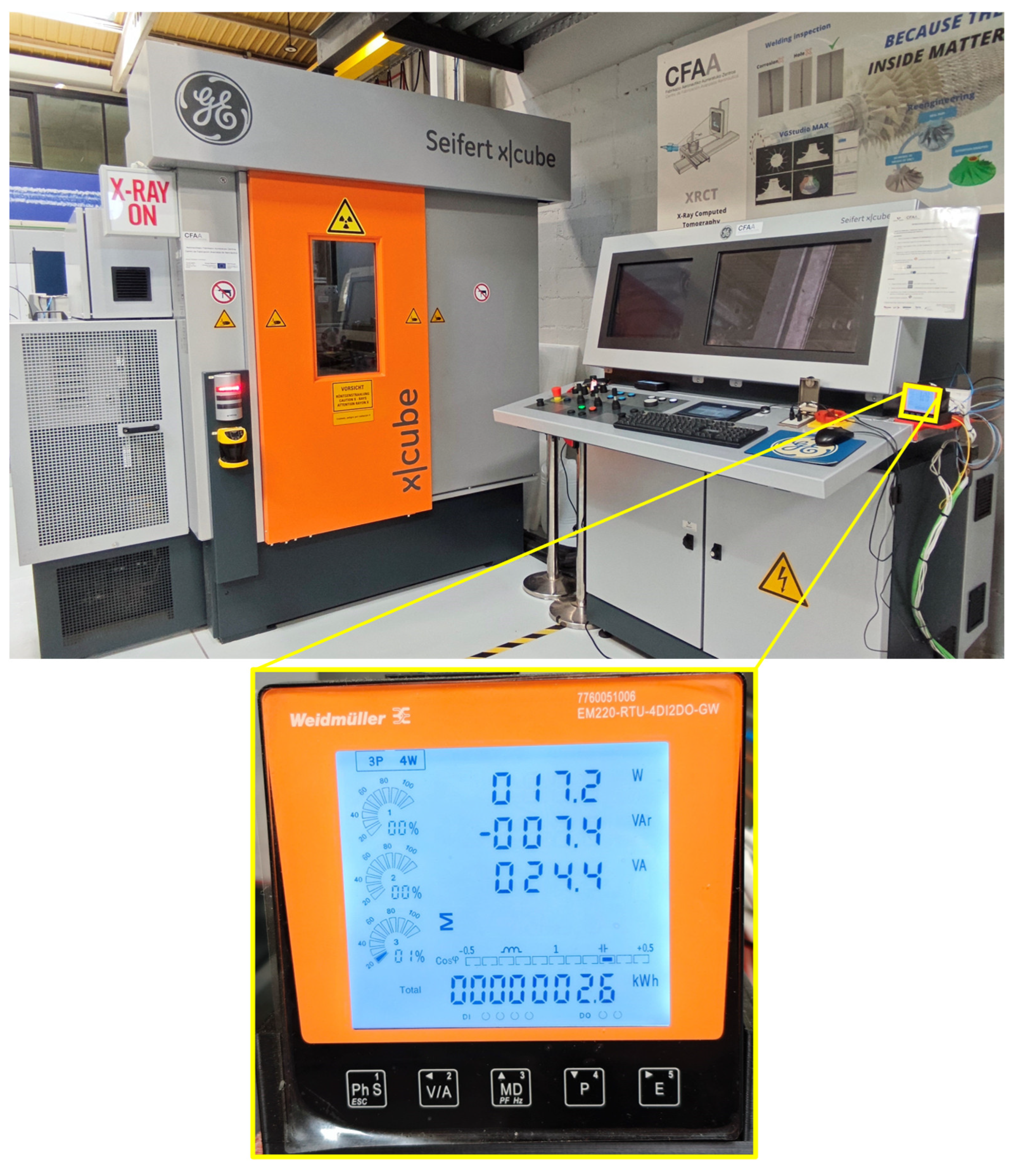
Beyond the need for accurate inspections, efficiency has become a crucial factor in CT applications. In today’s industrial landscape, the need to reduce scan time and energy consumption is imperative to align with sustainability goals. Shorter scan times enhance production and are supportive in reducing costs whilst also addressing sustainability by less energy use and low environmental effect. With this information, the challenge now lies in speeding up scan times without compromising data quality and, at the same time, avoiding significant increases in energy consumption.
Among these complexities, it cannot be overlooked that parameters are important regarding performance in CT. Parameters such as voltage, tube current, or exposure time have their influence on the scanning duration, the quality of the data obtained, and the energy expended. Understanding the interplay of these parameters is a crucial step towards optimizing the potential of CT for Non-Destructive Testing and for accurate dimensional measurements.
Various approaches have been developed regarding the CT scanning process optimization challenge. In this context, Reiter et al. [
5] propose a simulation-based approach to optimize CT scanning parameters. The findings demonstrate how simulation may predict optimal parameters before actual scans, also reducing the need for physical tests, enhancing industrial CT’s sustainability. Nevertheless, simulating CT processes is a complex task, since they are influenced by a large number of factors making it difficult to achieve realistic data.
An alternative approach is presented by Bellens et al. [
6], in their review on the application of machine learning techniques in industrial CT. The authors describe how Artificial Intelligence-based machine learning techniques may determine optimal acquisition parameters and scanning trajectories by learning from previous successful scans. Data-driven approaches enable the analysis of complex relationships between material properties, geometrical features, and scanning parameters. Conventional methods might overlook these interactions. This approach enhances efficiency by eliminating the need for trial-and-error testing.
However, in spite of the advances in parameter optimization, the literature shows a gap regarding the actual measurement and analysis of CT energy consumption. Addressing this gap is essential as energy efficiency has become a crucial aspect in industrial environments. For instance, although not explicitly demonstrated in industrial CT applications, recent research by Fenerich et al. [
7] provides an updated review of energy efficiency in industrial settings, highlighting strategies used to reduce energy consumption while keeping quality up.
The primary objective of this study was to evaluate the impact of CT parameters such as voltage, step size, and the number of radiographies per step (RPS) on scan time, data quality, and energy efficiency, using real energy consumption data. This work focuses specifically on enhancing performance in NDT inspection by obtaining high-quality measurements without excessively increasing energy consumption, while quantifying the relationship between these factors. By systematically analyzing these parameters, this study aims to identify those with the greatest influence and optimize their configuration for improved overall performance.
Additionally, this research emphasizes energy efficiency through detailed consumption measurements for CT procedures, making it particularly relevant in understanding the environmental impact of CT inspections. This approach aligns with the United Nations Sustainable Development Goals, which include ensuring sustainable consumption and production patterns [
8].
To sum up, the goal is to facilitate informed decision-making in the setup of CT parameters, advancing the field of Non-Destructive Testing and dimensional measurement in terms of both accuracy and sustainability.
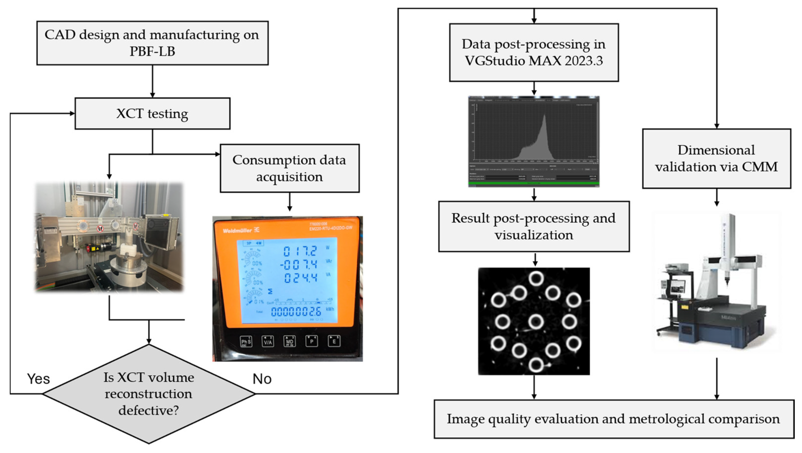
3. Results
Within this section, the results of the experiments are examined, with a focus on establishing connections between image quality enhancement and the corresponding increase in energy consumption caused by the modification of input parameters. As it is previously said, the major concern was to establish a proper balance between energy consumption and image quality to increase efficiency without compromising environmental sustainability objectives.
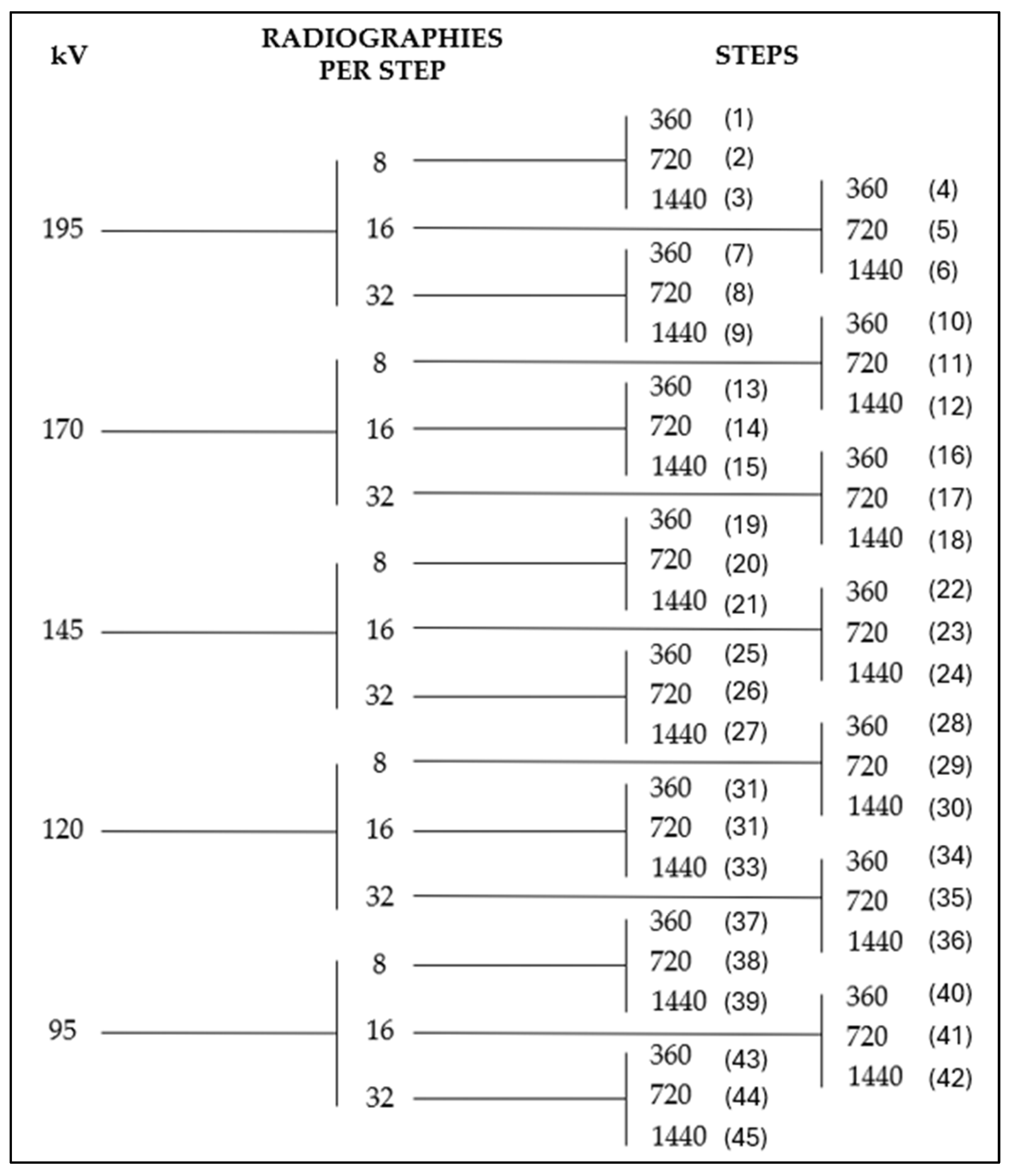
Table 1 shows the mean values and standard deviations (Std. Dev.) for each output parameter, calculated based on voltage variations. The four output parameters mentioned above are presented to evaluate both quality and power (P) consumption across the test configurations. For detailed visualization, several individual scan results are portrayed in subsequent figures where specific examples are graphically represented.
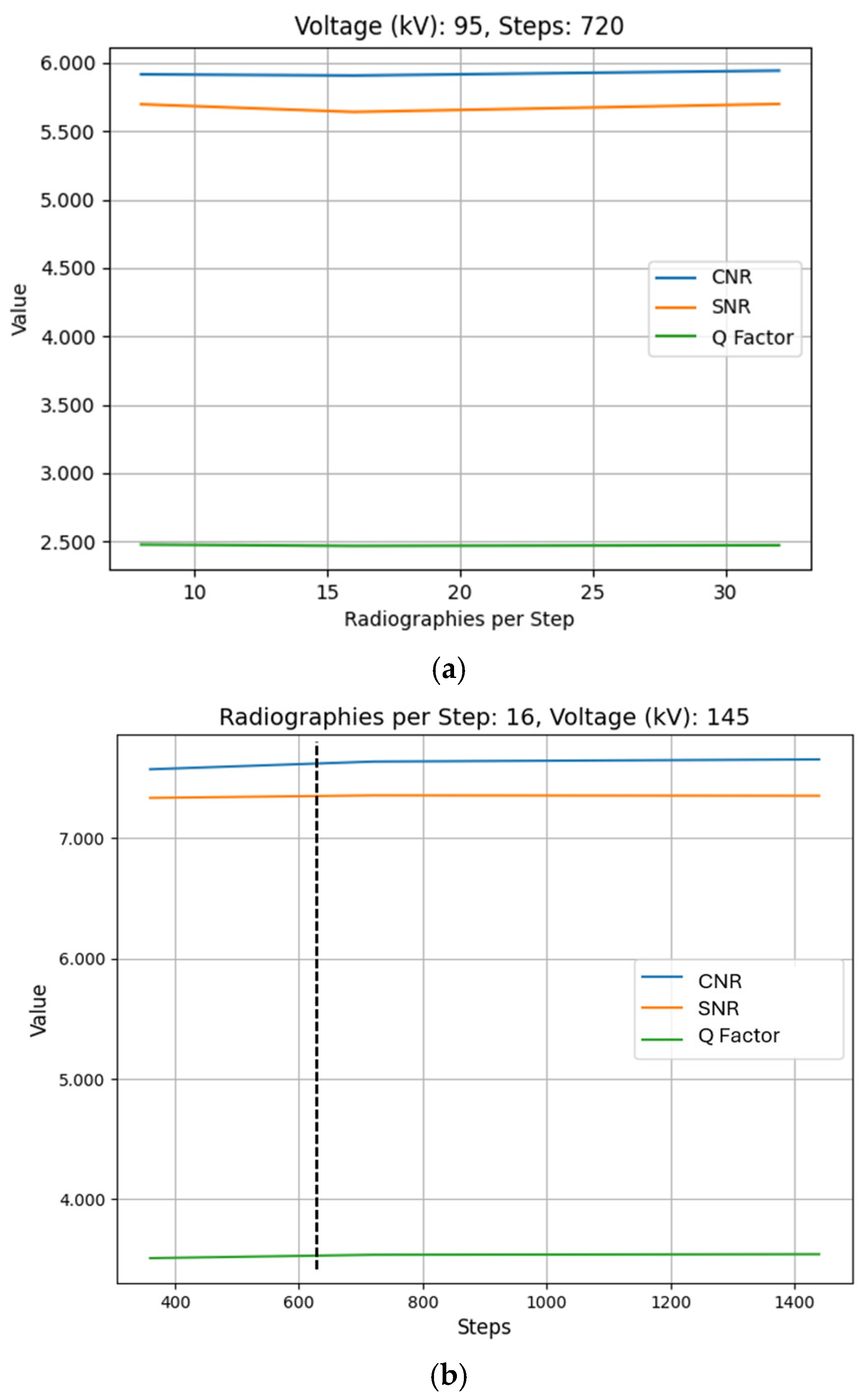
After conducting the experiments and analyzing the obtained results, although some variation is observed across different scan steps and RPS values, the changes in image quality metrics (CNR, SNR, Q) remain below 2% of their corresponding values. As illustrated in
Figure 9, varying these parameters shows that the quality parameters remain virtually constant across different combinations. The graphs for quality metrics against every parameter combination were generated. And, after observing the similarities, the graphs corresponding to test IDs 38, 41, and 44 in the first place, and 22, 23, and 24 in the second place are shown:
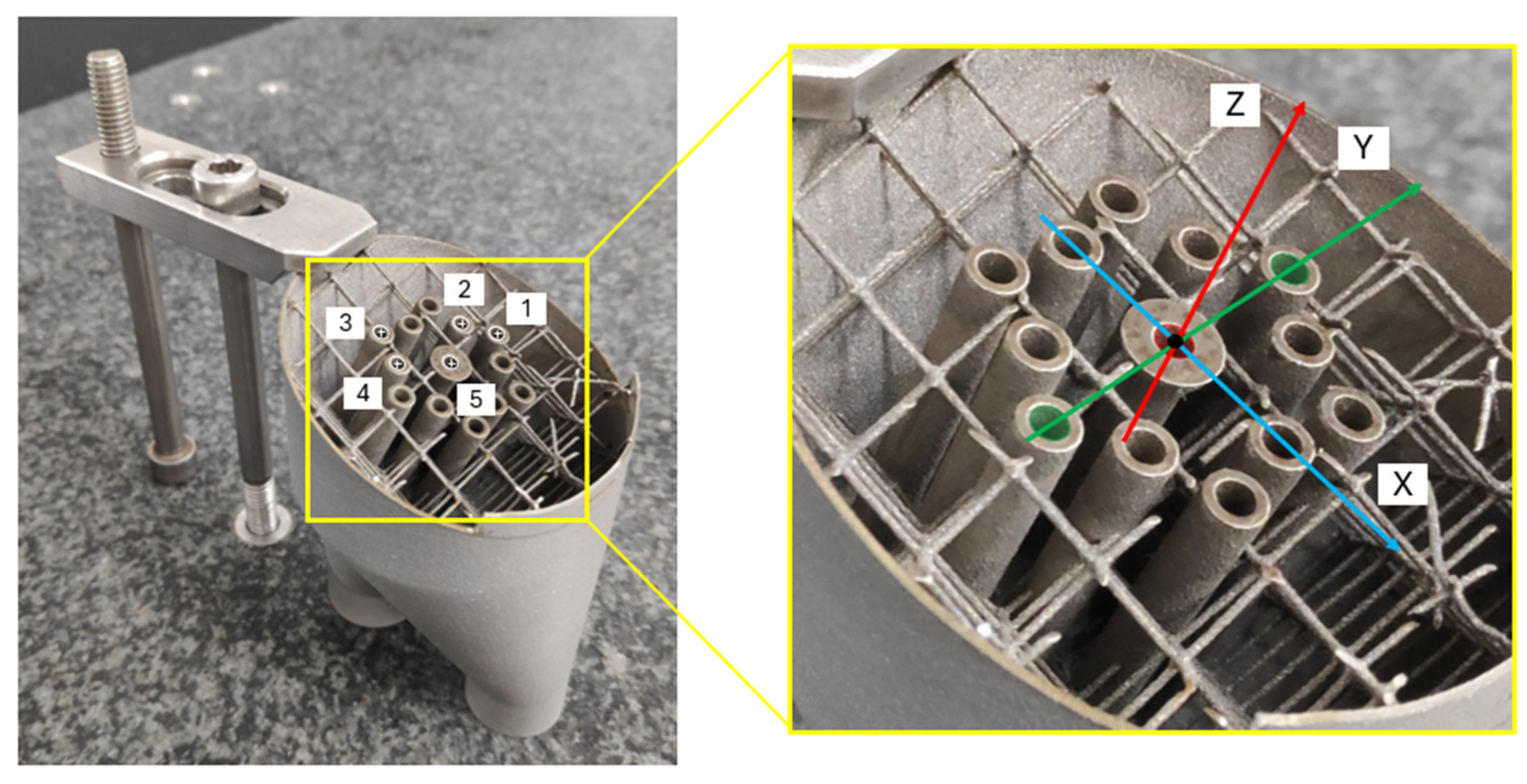
Each number of steps generates a displacement of the outer part of the specimen depending on the rotated angle and the dimensions of the specimen. A dotted line has been added with the purpose of indicating the value of steps needed for the specimen to fulfill a displacement equal to the resolution of the scans, which is a voxel size of 0.155 mm3. The number of steps needed to achieve that displacement is, specifically, 612.76 steps.
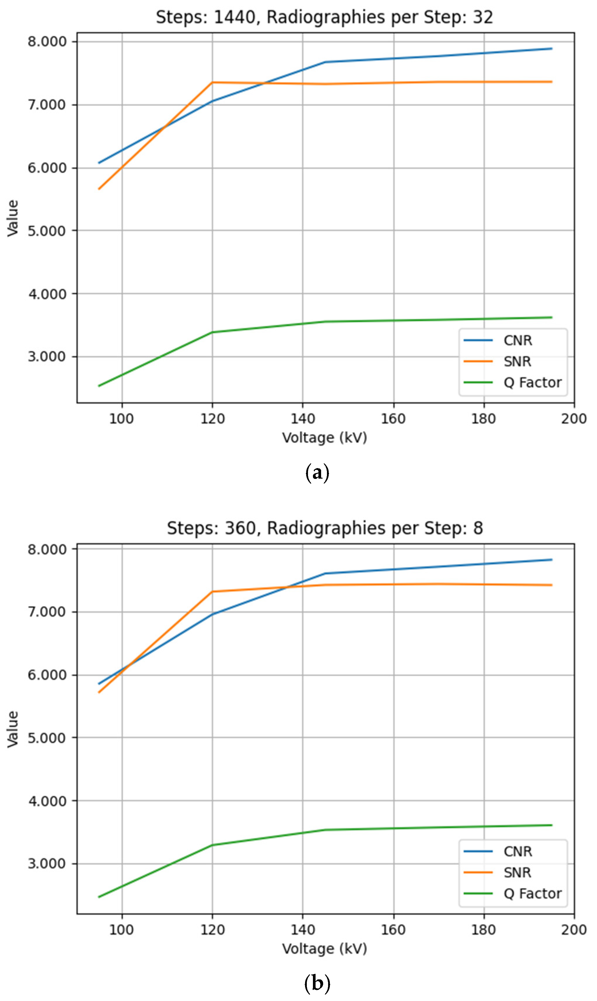
Moreover, the impact of voltage variation on image quality was assessed and deeper understanding was gained. The results indicate a uniform improvement across all quality metrics in relation to the increase in the voltage values. As demonstrated by the graphs shown in
Figure 10, where, again, after observing the similarities between the obtained graphs, the graphs corresponding to test IDs 9, 18, 27, 36, and 45 in the first place, and 1, 10, 19, 28, and 37 in the second place are shown in order to demonstrate the pattern.
One notable observation, in addition to the consistent quality enhancement across all parameters as voltage increases, is that not all parameters follow the same pattern. The CNR parameter exhibits the greatest sensitivity and variability, as it demonstrates the largest value increase. Moreover, it is evident that CNR experiences more substantial increments in the lower voltage transitions (95 to 120 and 120 to 145 kV). For the higher voltage increments (145 to 170 and 170 to 195 kV), the CNR increase is more modest. In contrast, the Q metric exhibits the least sensitivity to voltage variations, following a similar pattern. In the case of SNR, a substantial increase is observed in the transition from 95 to 120 kV; however, the increase gets milder for subsequent voltage increments.
A qualitative comparison between two different voltage level XCT images is shown in
Figure 11, where the improvement in image quality can be attributed to the greater X-ray penetration capacity of higher voltage configurations.
After analyzing the influence of different parameters on image quality, a detailed study of the relationship between CNR and voltage was conducted, as voltage demonstrated to be the most influential parameter on quality metrics. The following graph presents the average CNR values obtained for each voltage level. It also shows a trendline adjustment of the curve to an exponential curve fit, due to the previously seen trend of the CNR values reaching a plateau meaning that X-ray penetrability is maxed out.
The graph in
Figure 12 depicts the evolution of CNR as a function of the applied voltage, where each data point represents the average CNR value for a given voltage level. CNR rises with voltage, but the rate of increase diminishes at higher voltages. CNR exhibits substantial increments of 17.273% and 9.379% for the voltage transitions from 95 kV to 120 kV and 120 kV to 145 kV, respectively. However, for the higher voltage increments from 145 kV to 170 kV and 170 kV to 195 kV, the CNR improvements are relatively modest, at 1.457% and 1.452%, respectively.
Further analysis was conducted on the relationship between CT image quality and energy consumption. A new graph is shown below illustrating the connection between applied voltage, working power, and overall energy consumption. As may be seen, time is the main influencing parameter of total energy consumption, with all voltage slopes being remarkably similar. However, subtle increases in slopes are noticed as voltage progressively increases, indicating a slight rise in the equipment’s unit working power. Anyways, these changes do not represent a substantial influence on overall energy consumption.
The graph in
Figure 13 depicts the connection between applied voltage, working power, and overall energy consumption. Notably, although increasing the input voltage raises the unit power consumption (as evidenced by the steeper ascending directions of the data points for each voltage in the Time vs. Energy Consumption plane), it also shortens the exposure time needed considerably. This phenomenon is evident in the graph, where at higher voltages, although unit consumption is greater, the overall energy consumption is much lower.
Going on with the results analysis,
Figure 14 presents the relationship between CNR and energy consumption for each voltage value. The data show that, although higher energy consumption yields an improvement in CNR for every voltage value, that increment is very slight. The graph displays distinct curves for each voltage value, with multiple data points representing different exposure time configurations.
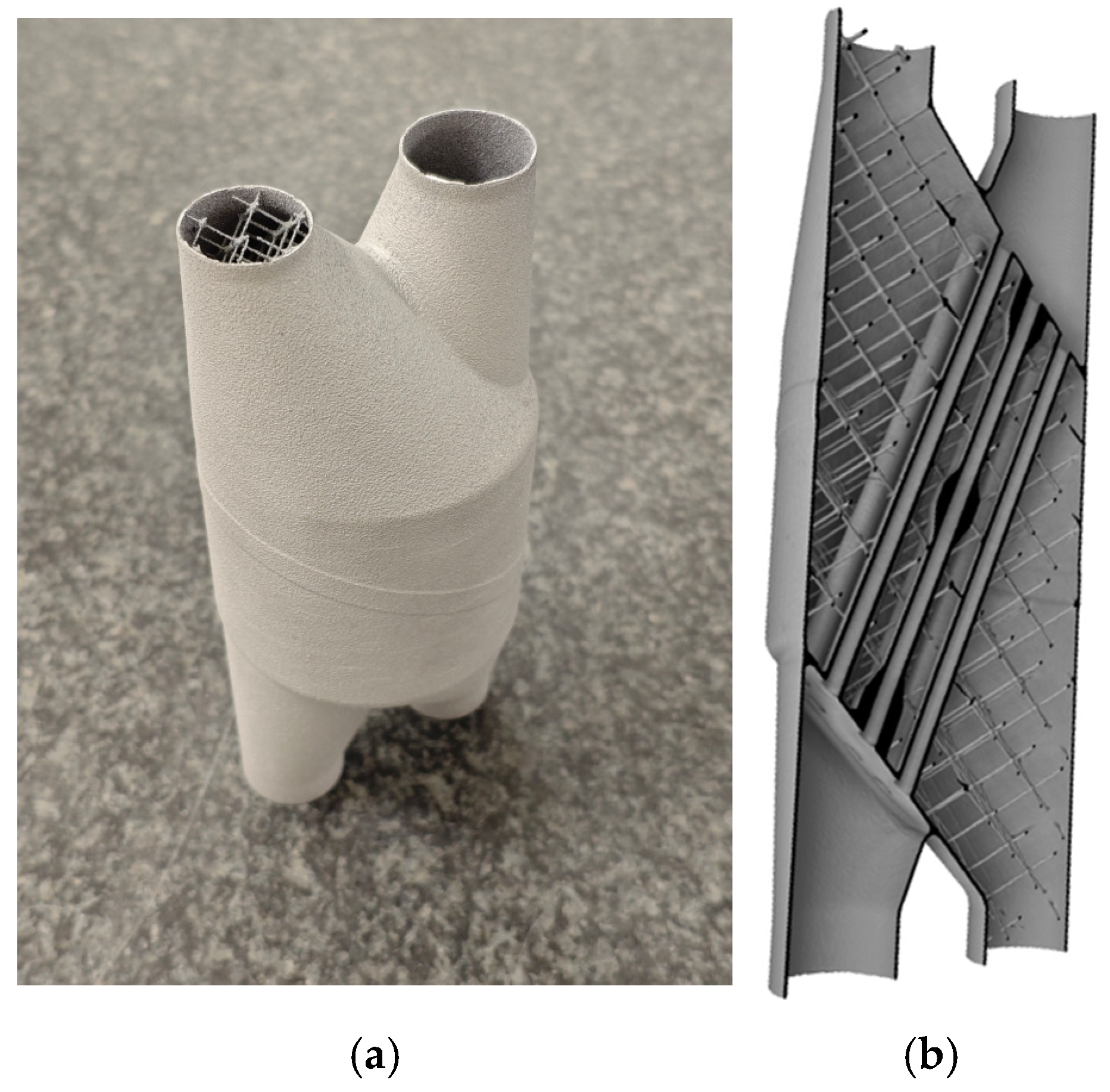
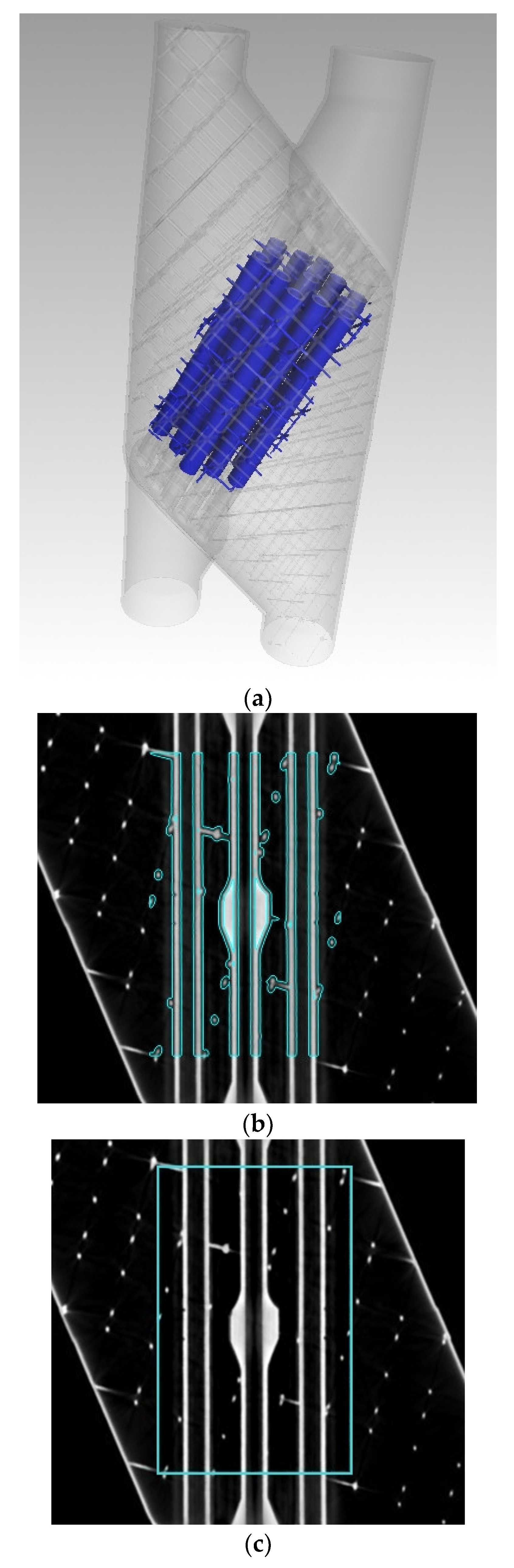
In the other hand, regarding the measurements made on the sample both on CMM and CT, the results obtained are shown in the following tables. The CMM measurement results are displayed first, in
Table 2, showing the mean values and standard deviations of diameter (D) and roundness deviation (Rd. Dev.) for each hole, calculated from 8 measurement repetitions.
Next, the results obtained from the CT measurements are displayed, mainly showing the diameter and roundness deviation of each hole, in
Table 3 and
Table 4 respectively. The CT tests used for this task were the ones with the following IDs: 5, 14, 23, 32 and 41. These specific tests were chosen because voltage was identified as the most influential parameter, so varying the voltage while keeping the other parameters constant was preferred. All circles were obtained using the Gauss (least squares) method.
Before continuing, it is important to note that it was not possible to obtain the values from CT test 41 because, due to the lack of penetration capability of the X-rays at 95 kV, VGStudio MAX surface definition tool was not able to detect any surfaces in the inside part of the central hole. Therefore, making it impossible to align the part following the same method as in the CMM.
Derived from the data presented in the tables, several comparative analyses were carried out between the data extracted from the CMM and the data extracted from the CT scans. The objective of these analyses was to focus on the degree of agreement between the two approaches, focusing on the discrepancies or similarities of the extracted values.
Firstly, the comparison between the hole diameters was conducted. The comparison is displayed in the following graph:
The diametral measurements performed on the 5 holes in both techniques are illustrated in
Figure 15. At first glance, a nuanced pattern may be seen. Notably, the values obtained from the 120, 145, and 170 kV CT scans show an almost identical trend amongst them. Indeed, the mentioned trend also aligns closely with the CMM measurements, with the exception of hole 3. However, the 195 kV CT scan shows a different behavior. It matches the trend of the CMM measurements more closely, with the exception of hole 1.
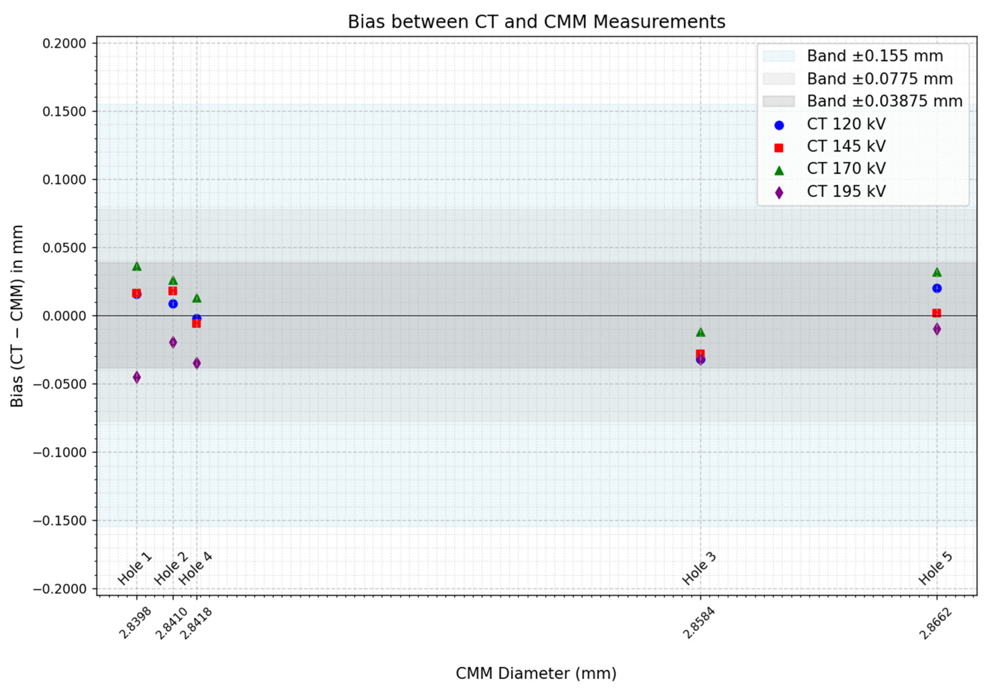
In order to provide more information about the magnitude of the systematic differences between the two measurement techniques, the absolute bias between CMM and CT measurements was calculated. The results are shown in
Figure 16:
After calculating the bias between the measurements of both techniques, it could be observed that a similar trend to the one in
Figure 15 appeared. In addition, calculating the bias also made it possible to quantify the magnitude of the measurement discrepancies between techniques. The maximum error detected is approximately 45 μm, which is notably 4 times smaller than the 0.155 mm
3 voxel size of the tomographic scans. This indicates that, if discrepancies remain below voxel size, CT scanning lacks sensitivity to reliably detect subtle geometric variations like the ones in the examined features. Furthermore, the graph also includes reference bands corresponding to the voxel size, 50% of the voxel size, and 25% of the voxel size. Notably, all values fall within the voxel size limit but even within 50% of the voxel size, further reinforcing the resolution limitations of the technique.
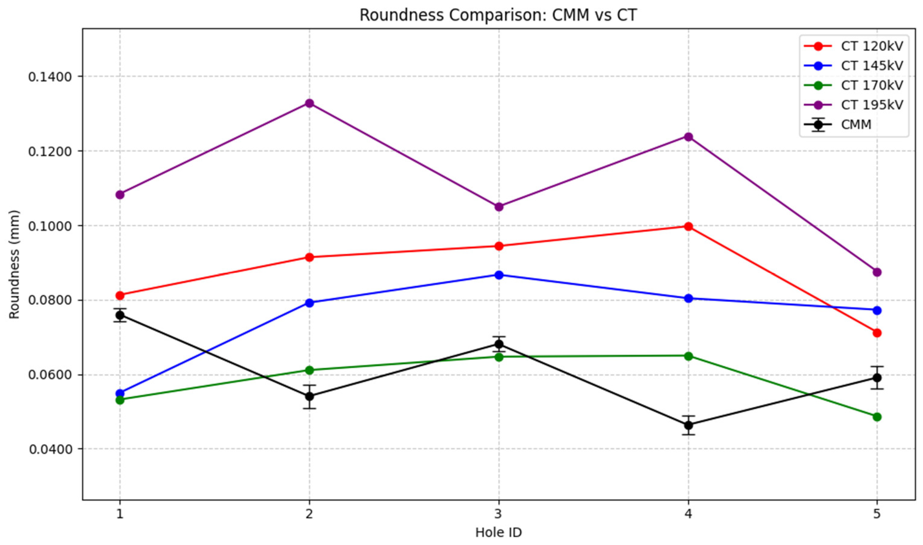
To provide additional insight, a graph comparing the roundness values of the holes in both techniques was created. The results are shown in
Figure 17:
Examining the graph in
Figure 17, it became obvious that the values of the 195 kV CT scan were consistently higher compared to the ones of the other voltage levels. However, the same happens as in
Figure 16, the obtained values remain below voxel size. Again, showing the resolution limitation for detecting such small feature variations.
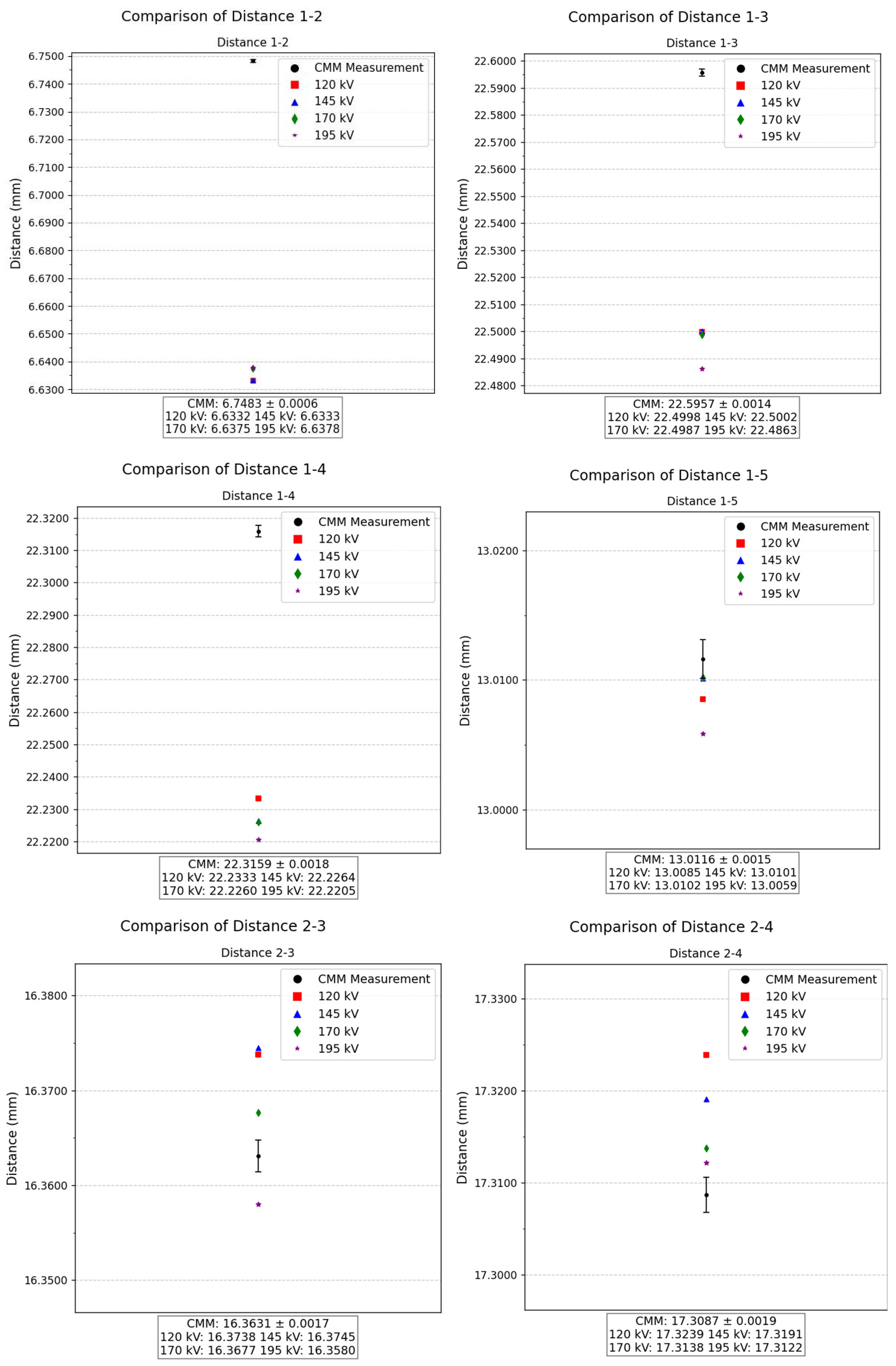
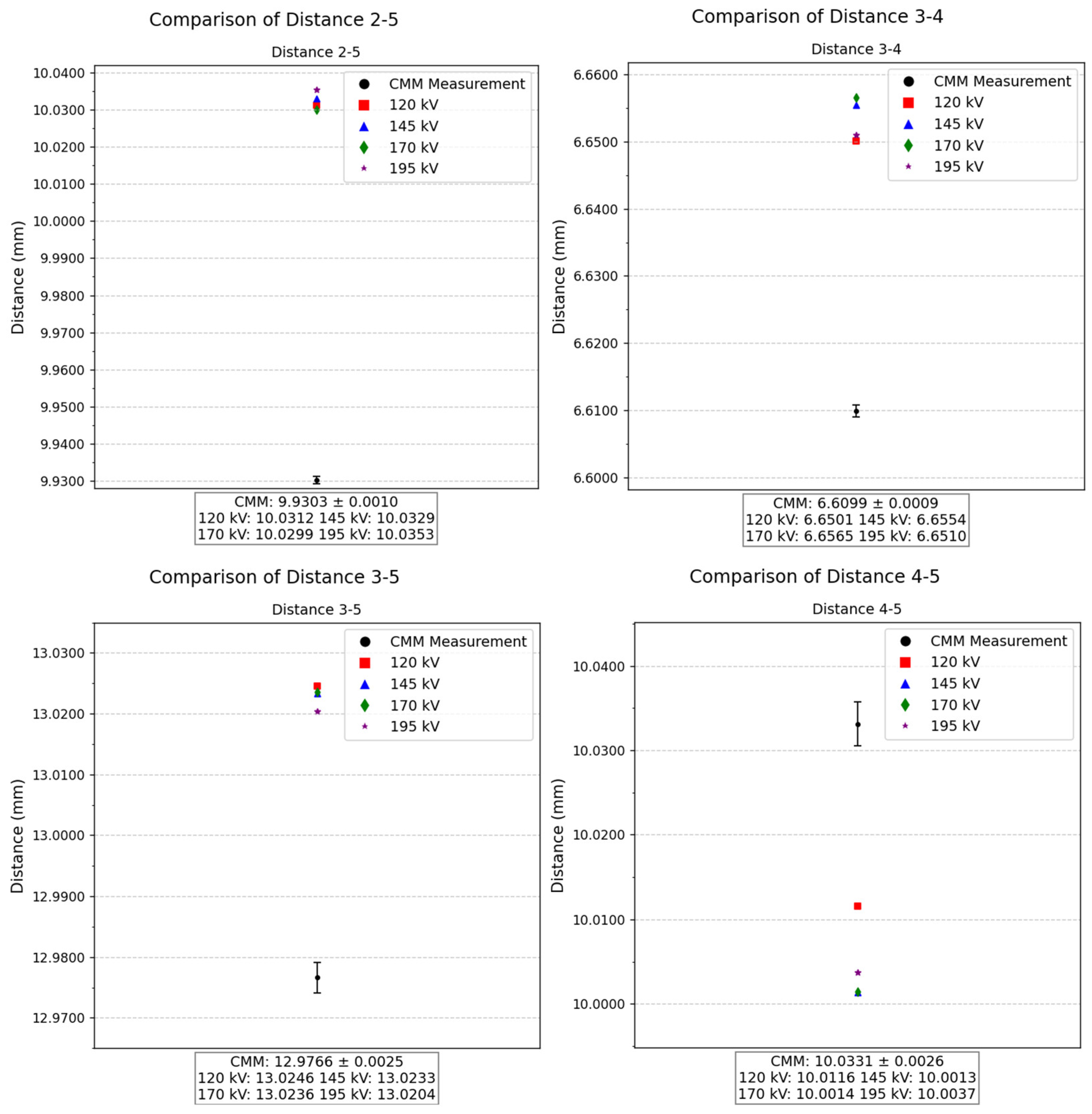
Regarding the distances between hole centers, measurements were performed using both CT and CMM techniques for all combinations between holes. A total of 10 distances were analyzed, covering combinations such as 1–2, 1–3, 1–4, 1–5, 2–3, 2–4, 2–5, 3–5, and 4–5. For each case, an individual plot was created in the
Figure 18 showing the CMM reference and corresponding CT measurements, allowing direct comparison of deviations.
The analysis of the 10 measured distances reveals no consistent trend in the comparison between the CMM and CT techniques. In some cases, such as the distance between 1–5 holes, the difference between both techniques is on the order of 1 µm. Nevertheless, the difference of the two techniques reaches approximately 100 µm in the case of the distance between 1–2 holes. Despite these variations, the differences between CT measurements remain stable, never exceeding approximately 10 µm across all cases. This pattern indicates that the CT-based measurements maintain a high level of consistency.
4. Discussion
After obtaining the experimental results from the tests, in this section these results are analyzed regarding the influence of different input parameters on CT image quality and system efficiency. In the first place, the lack of influence of RPS and steps parameters on image quality (
Figure 9) is highlighted. The impact of these parameters on image quality metrics remains minor, as evidenced by the standard deviations observed in
Figure 9. In
Figure 9a, the CNR, SNR, and Q exhibit standard deviations of 0.018, 0.033, and 0.005, respectively. Similarly, in
Figure 9b, the standard deviations are 0.043 for CNR, 0.011 for SNR, and 0.018 for Q. These low variations indicate that the influence of RPS and steps on image quality is minimal compared to other parameters such as voltage.
This behavior can be attributed to the physical limitations of the reconstruction process. The rotational step displacement produced by each step is of similar magnitude to the reconstructed voxel size of the tomographic data. Specifically, in the configuration with 360 steps, which represents the scenario with the largest displacement per step, the displacement value reaches 0.262 mm in the outer region of both ROIs. Since this displacement is comparable to the voxel dimensions of 0.155 mm, the volume generation algorithm cannot discern notable differences during reconstruction, as the incremental changes are equivalent to the spatial resolution of the data. For configurations with higher step counts, the displacement per step decreases further, reaching values as low as 0.066 mm, which is significantly below the system’s voxel size. This explains why increasing the number of steps does not lead to improved image quality. This limitation is particularly relevant in micro-CT and nano-CT systems, where smaller voxel sizes make step displacement effects more pronounced, requiring careful optimization of scanning parameters. It is expected that lowering the number of steps would result in a decrease in image quality, which may be slightly inferred from the CNR values in
Figure 9b, as the displacement would become considerably bigger than the voxel size.
The voltage parameter, however, has demonstrated a significant impact on image quality, as shown in
Figure 10. It may be seen that, even though every metric’s value increases with voltage, each metric reacts in slightly different ways when subjected to voltage variations. CNR is the parameter that exhibits the highest sensitivity to voltage changes, particularly at the lower end of the voltage range used in the tests. This enhanced sensitivity at lower voltages implies that the initial increases in voltage (95 to 145 kV) provide the most substantial improvements in image contrast and noise reduction. The decreasing rate of improvement at higher voltages (145 to 195 kV) indicates an approach to an optimal voltage range for the specimen under study. The SNR parameter shows a similar pattern, reaching a plateau after the initial voltage increase from 95 to 120 kV, suggesting that optimal signal-to-noise performance can be achieved at relatively lower voltage levels. As mentioned before, Q metric is the less sensitive metric out of the three analyzed metrics.
The analysis of CNR evolution with voltage (
Figure 12) provided the most decisive evidence for optimizing CT parameters. The CNR improvements were substantial in the lower voltage transitions: 17.273% for 95–120 kV and 9.379% for 120–145 kV. In contrast, higher voltage transitions showed minimal gains of approximately 1.45% (for both 145–170 kV and 170–195 kV). These results clearly indicate that the higher voltage levels used in the trials approached the optimal range for maximizing CNR performance for the specimen under study. This saturation effect is attributed to the physical properties of the scanned specimen. Every object scanned in XCT has an accumulated thickness that the X-ray beam must penetrate, which depends on the applied tube voltage. As the voltage increases, the X-rays gain greater penetration power, allowing more material to be traversed effectively. However, once the voltage reaches a level sufficient to fully penetrate the sample, further increases provide only marginal improvements, as all regions of interest are already well-defined in the reconstructed image. Increasing the voltage results in a higher kinetic energy of the photons, which improves the material’s penetration capacity. Higher energy photons are less likely to be absorbed via the photoelectric effect, allowing them to travel through a greater thickness of material. The dominant interaction at higher energies is Compton scattering, where photons transfer part of their energy to outer-shell electrons, allowing the photons to continue through the material with reduced energy. Additionally, Rayleigh scattering plays a minor role, where photons are scattered without losing energy, but this interaction does not significantly affect penetration. Beyond a certain voltage, further increases in voltage lead to only slight improvements, as the material has already been adequately penetrated, resulting in a plateau in the CNR curve. This suggests that the optimal scanning voltage for the specimen has been reached, and additional energy input does not significantly enhance image quality. This finding was combined with energy efficiency considerations at 195 kV. At this voltage, shorter exposure times resulted in comparable overall energy consumption while maintaining the highest quality metrics. These factors positioned this voltage level as the optimal operating point when combined with reduced exposure times.
Regarding energy efficiency, the analysis of power consumption and exposure time (
Figure 13) revealed important relationships. Higher voltages increased the unit power consumption. However, they significantly reduced the required exposure time. This reduction resulted in lower overall energy consumption. For instance, at 195 kV with 360 steps and 8 RPS, the energy consumption was only 2.762 kWh compared to 7.106 kWh for the same configuration at 95 kV, representing a reduction of approximately 61% in energy usage. This finding is very interesting in terms of CT industrial operation optimization. That may be better explained by the relationship between CNR and energy consumption at different voltage levels (
Figure 14). While higher energy consumption per voltage increment does yield quality improvements, these gains are relatively modest. This implies that operating at shorter exposure times should generally prove beneficial with respect to productivity while not critically undermining image quality. Substantial differences may be found, by contrast with quality, in the values of energy consumption when increasing exposure time, as it may be seen in 145 kV scans, where CNR values vary from 7.605 to 7.669 while energy consumption values range from 3.043 kWh to 29.796 kWh. However, it is worth noting that selecting the absolute minimum exposure time may not always be necessary, because the middle points on each voltage curve could offer an acceptable balance between quality and efficiency.
Concerning the results obtained from the dimensional and geometrical measurements performed in CMM and CT technologies, several findings were made. The diameter measurements showed that CT scans displayed consistent trends across different scanning voltages, with values closely aligned to the CMM ones. Nevertheless, after calculating the bias between both techniques, it was observed that the variations remained below CT scan voxel size, suggesting that the resolution used lacks sensitivity to detect the features examined in the heat exchanger.
An interesting observation regarding hole 5 is that the cylinder wall thickness is greater compared to the thickness of the other 4 cylinders. This variation potentially explains the consistently larger diameter values observed across all scanning voltages in hole 5, as the structural variation might have influenced the penetration capability of the X-rays.
Roundness measurements inferred the same conclusion as before. It may be possible that the 195 kV scan values are higher due to the improved image clarity demonstrated before, as it could enable a better detectability of surface roughness. Anyways, the values remain below 0.155 mm voxel size, addressing the current resolution’s limitation to detect the variations of the current sample. As shown in
Figure 16, despite a substantial 62.5% increase in voltage from 120 kV to 195 kV, the observed dimensional variations remain within a range smaller than 25% of the voxel size. This suggests that, while voltage adjustments influence imaging parameters, their impact on dimensional accuracy is considerably less pronounced compared to their effect on image quality metrics, at least for this scenario. Consequently, improvements in sharpness or contrast due to higher voltage do not necessarily translate into significant enhancements in metrological precision, as the fundamental resolution limitation imposed by voxel size remains the dominant factor.
Future research could involve transitioning to micro-CT or nano-CT techniques in order to develop dimensional and geometrical study, as these techniques would be sensitive to data variations.


