
Low-Power and High-Performance Double-Node-Upset-Tolerant Latch Using Input-Splitting C-Element


Abstract
1. Introduction
2. Existing Hardened Latches
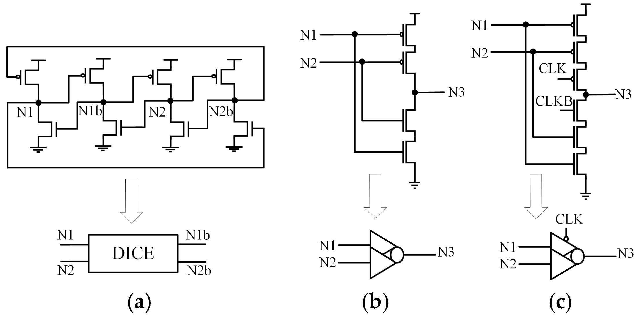
2.1. Dual Interlocked Storage Cell (DICE) and C-Element (CE)
2.2. CLCT
2.3. LPDHL
2.4. DCTELC
2.5. CDNUTC
2.6. HRDNUT
2.7. LSEDUT
2.8. DNUSH
2.9. LCDRL
2.10. DRLW
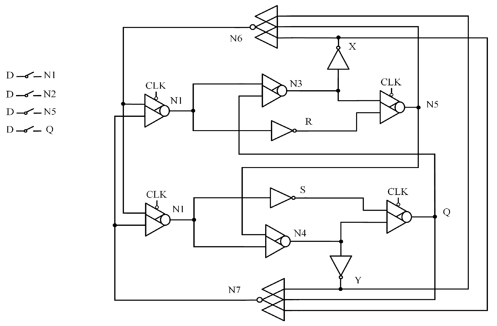
3. Proposed Hardened Latch Design
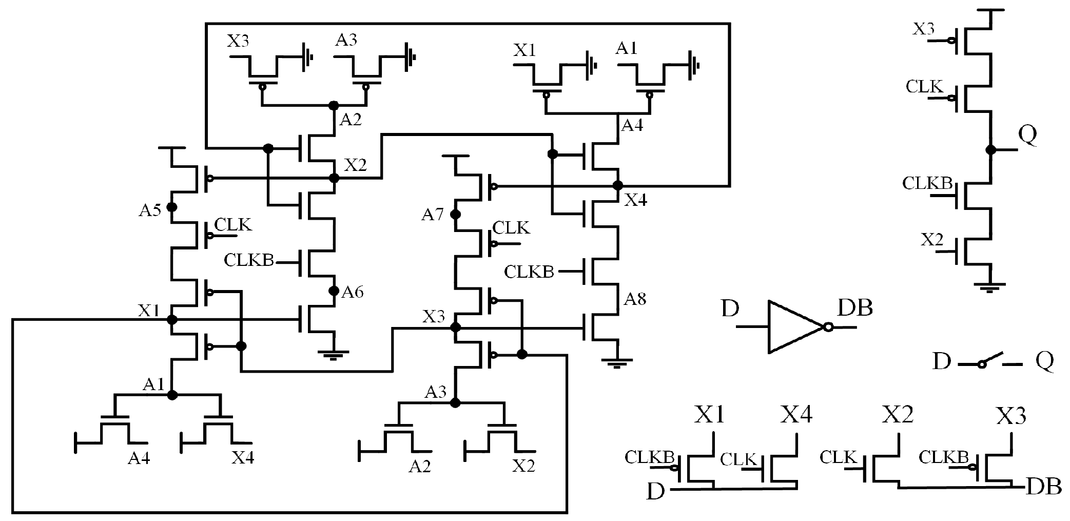
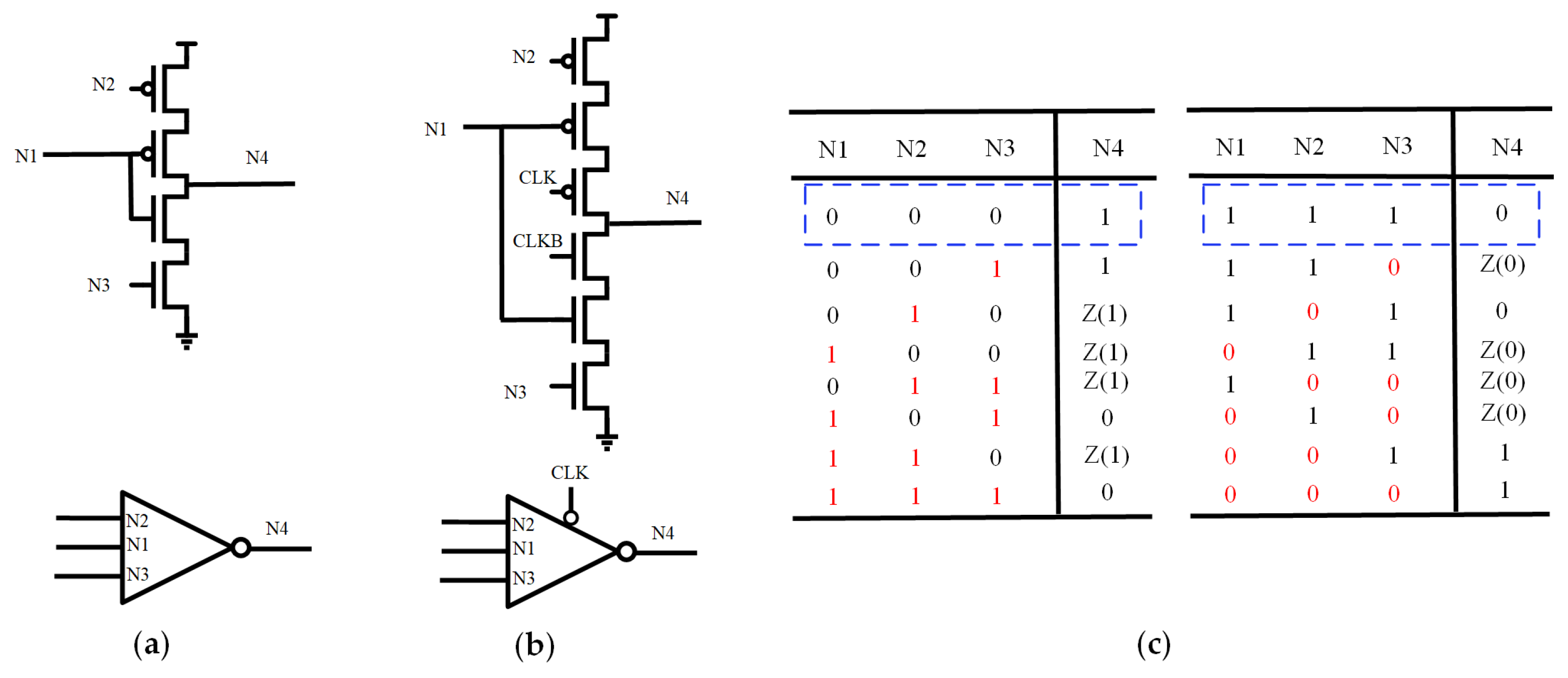
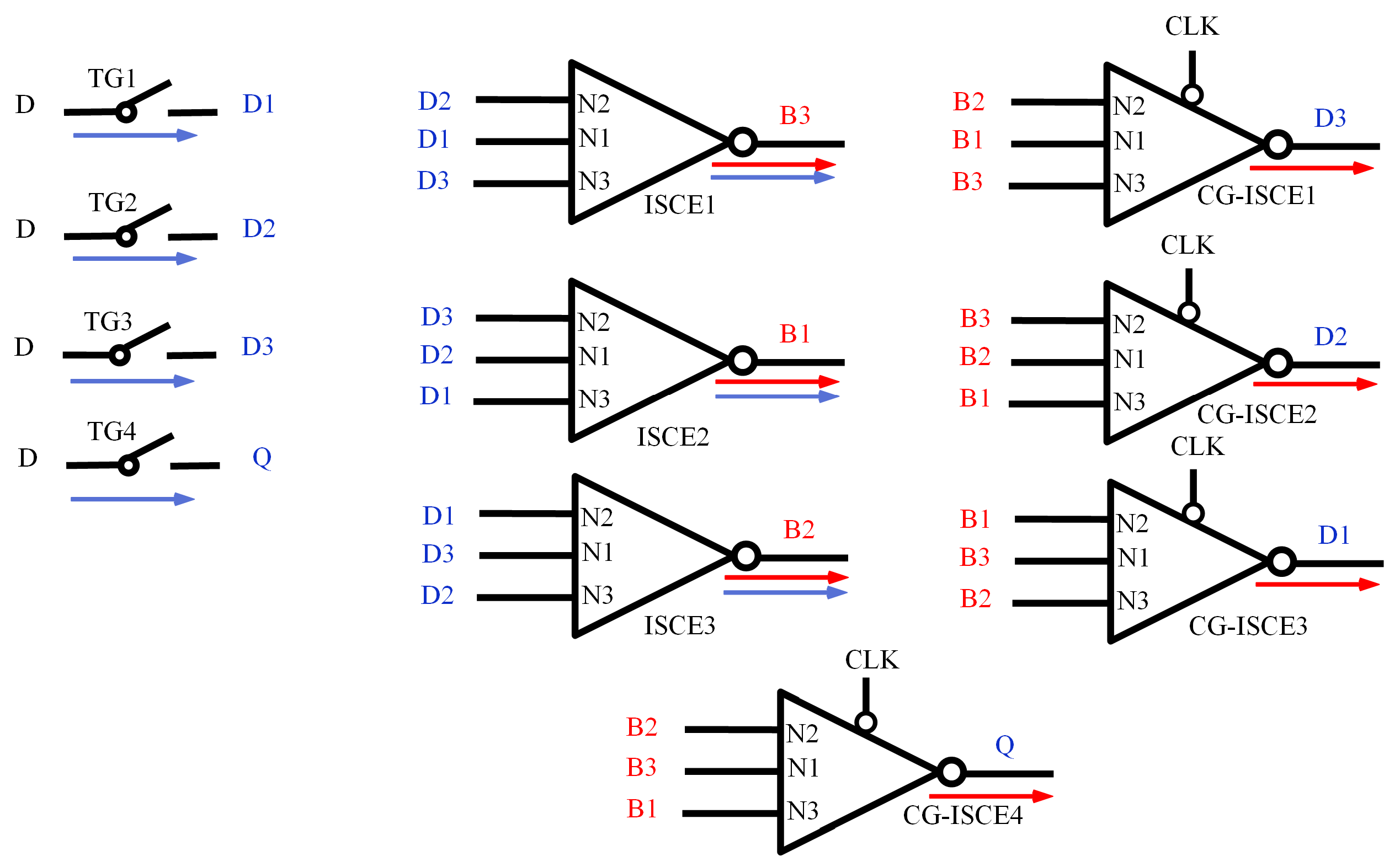
3.1. Working Principle of Input Splitting C-Element
3.2. Proposed DNU Tolerant Latch Design
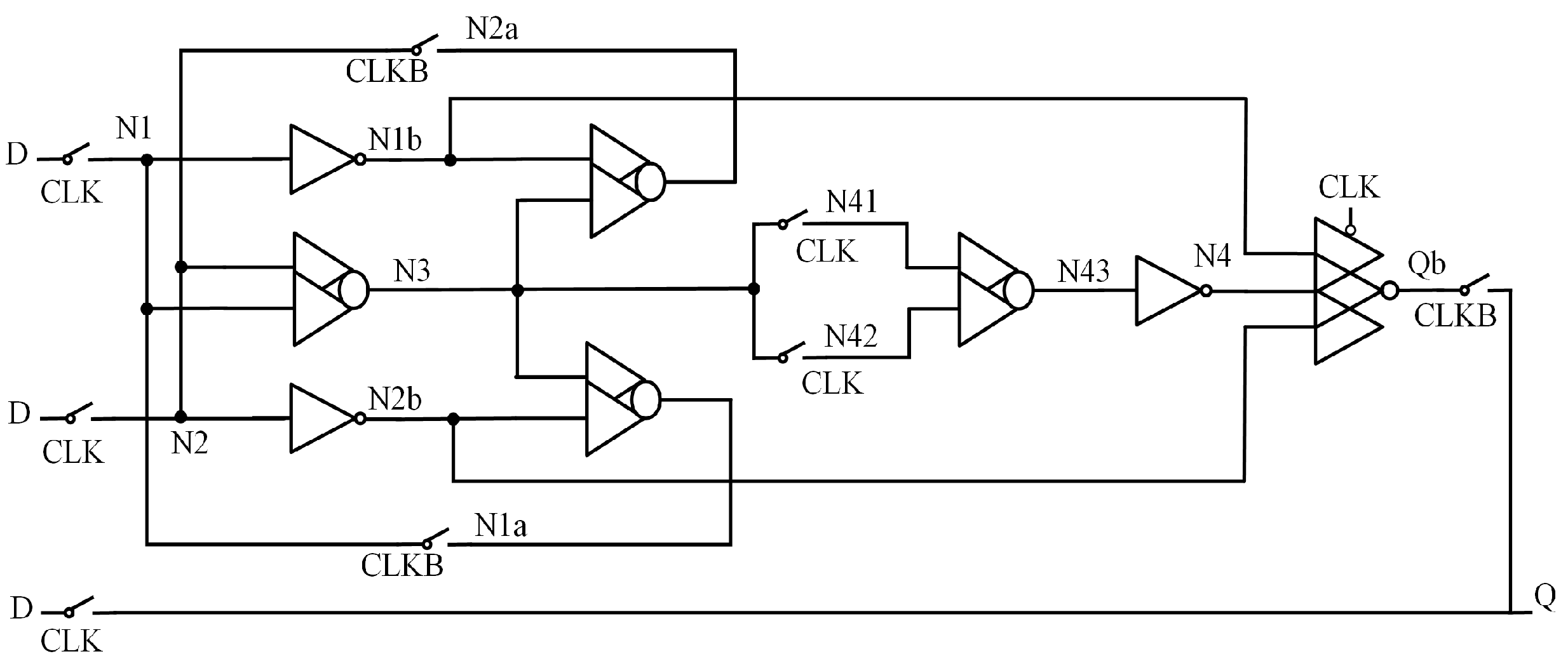
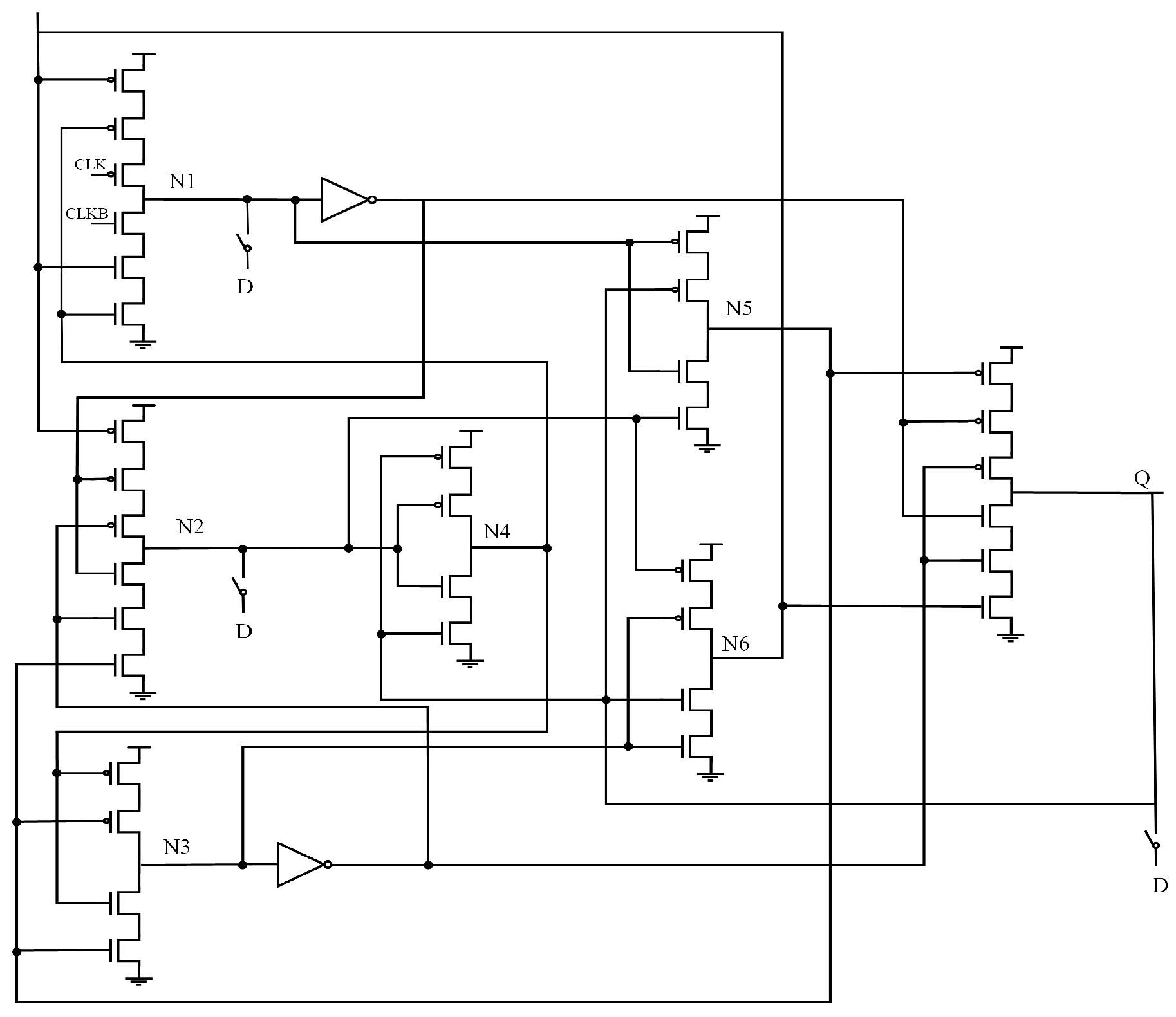
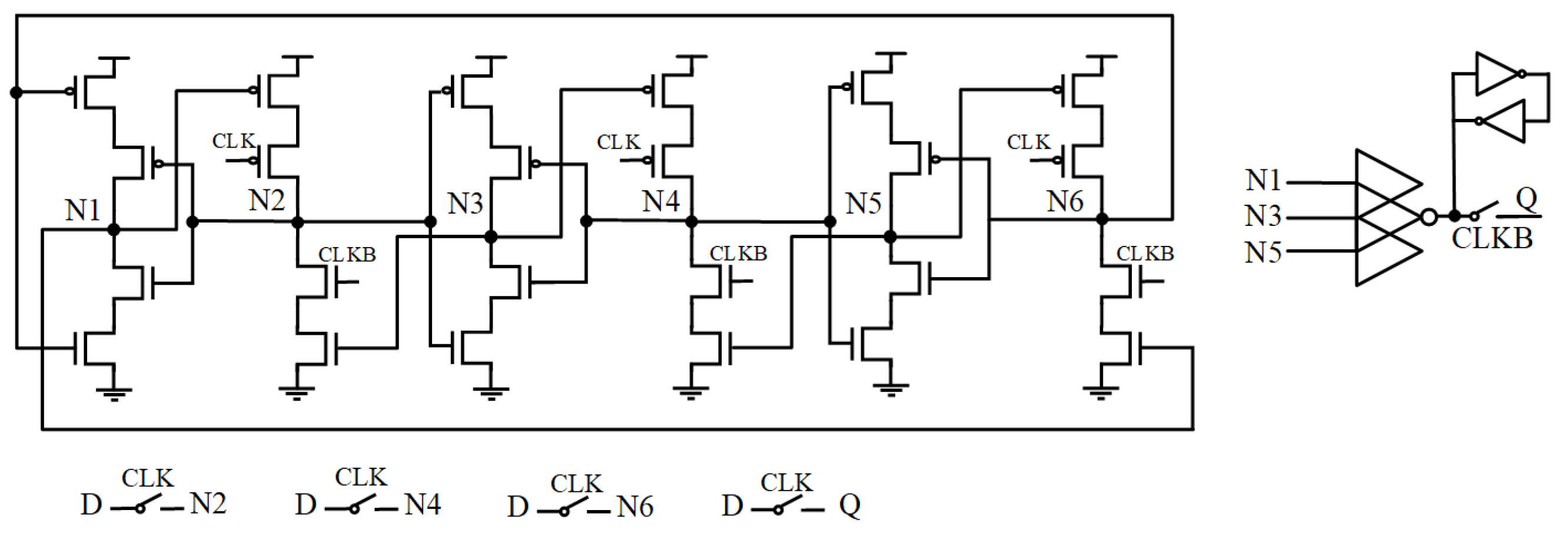
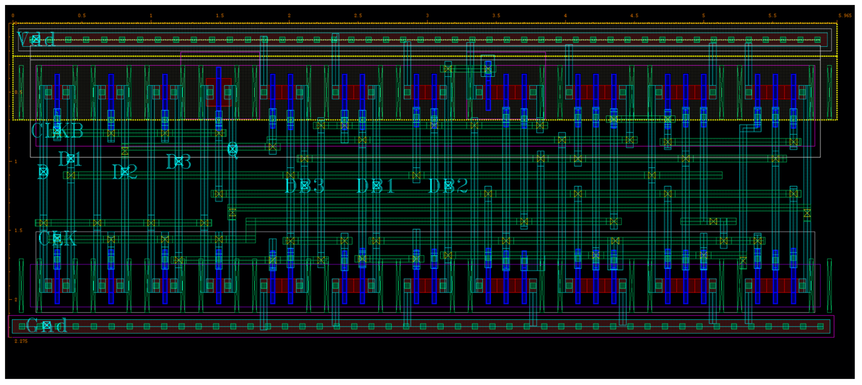
3.2.1. Circuit Structure
3.2.2. Working Principle
3.2.3. Hardening Principle
- (1)
- Q Flips, and One of D1–D3 or B1–B3 Flips: For instance, if <Q, D1> flips, the other nodes remain unaffected. From the SNU fault-tolerant analysis, D1 is restored by CG-ISCE3, and Q is then corrected by CG-ISCE4.
- (2)
- Two B Nodes Flip: There are two sub-cases:Q Flips and Self-Recovers: For example, when <B2, B3> changes from <1, 1> to <0, 0>, Q flips. CG-ISCE2 and CG-ISCE4’s pull-up circuits conduct, causing D2 and Q to change from 0 to 1. ISCE3 remains unaffected by D2. ISCE3’s pull-up circuit conducts, restoring B2 to 1. Then, CG-ISCE2’s pull-down circuit conducts, bringing D2 back to 0. ISCE1’s pull-up circuit restores B3 to 1. Consequently, D1–D3 and B1–B3 are all restored to their correct values, and Q is corrected by CG-ISCE4. A similar process occurs for <B1, B3>.Q Remains Unaffected: For example, when <B1, B2> changes from <1, 1> to <0, 0>, CG-ISCE1’s pull-up circuit conducts, causing D2 to change from 0 to 1. Due to CG-ISCE4’s interception, the output Q remains unaffected. In all other cases, Q does not flip.
- (3)
- Two D Nodes Flip: For instance, if <D1, D2> changes from <1, 1> to <0, 0>, ISCE1’s pull-up circuit conducts, causing B3 to change from 0 to 1. Due to CG-ISCE4’s interception, Q remains unaffected. The mechanisms for <D1, D3> and <D2, D3> are analogous. Additionally, when <D2, D3> flips, self-recovery is achieved through the feedback loops of ISCE1–3 and CG-ISCE1–3.
- (4)
- One D Node and One B Node Flip: Since an ISCE’s output is affected only when both inputs experience faults, the other nodes remain unaffected. Therefore, Q remains unchanged.
3.3. Fault Injection Experiment
4. Simulation Results
4.1. Performance Comparison of Latches
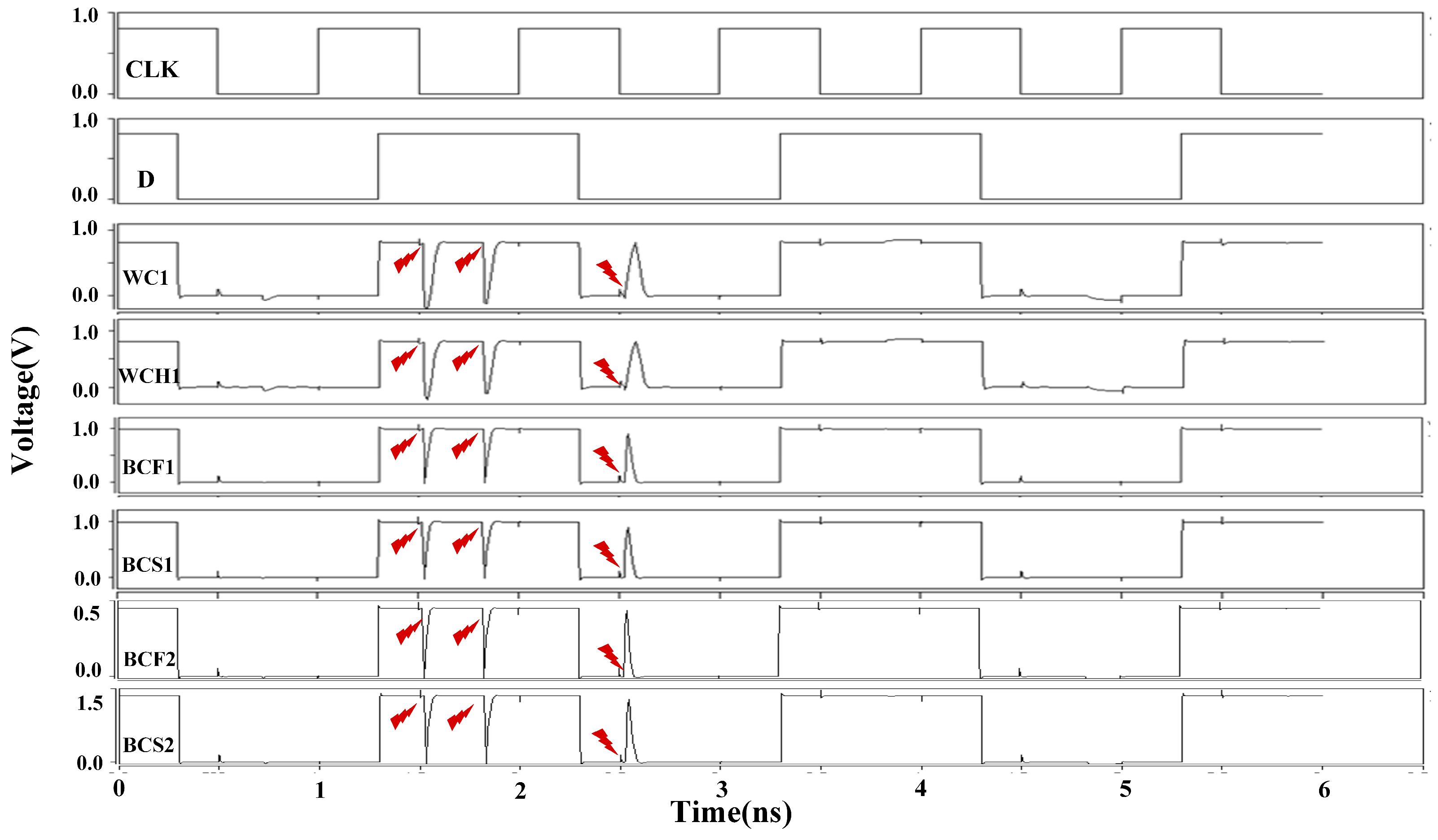
4.2. Effect of PVT Variations on Latches
5. Conclusions
Author Contributions
Funding
Institutional Review Board Statement
Informed Consent Statement
Data Availability Statement
Conflicts of Interest
References
- Automotive Electronics Council. AEC-Q100-Rev-J. Failure Mechanism Based Stress Test Qualification for Integrated Circuits. 2023. Available online: http://www.aecouncil.com/AECDocuments.html (accessed on 21 January 2025).
- Ro, D.; Um, M.; Lee, H.-M. A Soft-Error-Tolerant SAR ADC with Dual-Capacitor Sample-and-Hold Control for Sensor Systems. Sensors 2021, 21, 4768. [Google Scholar] [CrossRef] [PubMed]
- Dai, Y.; Yang, Y.; Jiang, N.; Qi, P.; Chen, Q.; Tong, J. A High Performance and Low Power Triple-Node-Upset Self-Recoverable Latch Design. Electronics 2022, 11, 3606. [Google Scholar] [CrossRef]
- Guo, J.; Liu, S.; Zhu, L.; Lombardi, F. Design and Evaluation of Low-Complexity Radiation Hardened CMOS Latch for Double-Node Upset Tolerance. IEEE Trans. Circuits Syst. I 2020, 67, 1925–1935. [Google Scholar] [CrossRef]
- Huang, Z.; Zhang, Y.; Su, Z.; Liang, H.; Yao, H.; Ni, T. A Hybrid DMR Latch to Tolerate MNU Using TDICE and WDICE. In Proceedings of the 2018 IEEE 27th Asian Test Symposium (ATS), Hefei, China, 15–18 October 2018; pp. 121–126. [Google Scholar]
- Jiang, J.; Zhu, W.; Xiao, J.; Zou, S. A Novel High-Performance Low-Cost Double-Upset Tolerant Latch Design. Electronics 2018, 7, 247. [Google Scholar] [CrossRef]
- Yano, K.; Hayashida, T.; Sato, T. Analysis of SER Improvement by Radiation Hardened Latches. In Proceedings of the 2012 IEEE 18th Pacific Rim International Symposium on Dependable Computing, Niigata, Japan, 18–19 November 2012; pp. 89–95. [Google Scholar]
- Black, J.D.; Dodd, P.E.; Warren, K.M. Physics of Multiple-Node Charge Collection and Impacts on Single-Event Characterization and Soft Error Rate Prediction. IEEE Trans. Nucl. Sci. 2013, 60, 1836–1851. [Google Scholar] [CrossRef]
- Ahlbin, J.R.; Gadlage, M.J.; Atkinson, N.M.; Bhuva, B.L.; Witulski, A.F.; Holman, W.T.; Massengill, L.W.; Eaton, P.H.; Narasimham, B. Effect of Multiple-Transistor Charge Collection on SET Pulse Widths. In Proceedings of the 2010 IEEE International Reliability Physics Symposium, Garden Grove, CA, USA, 2–6 May 2010; pp. 198–202. [Google Scholar]
- Chen, Z.; Xie, Y.; Liang, J.; Bi, D.; Hu, Z.; Zhang, Z. An Ultra Low-power Double-node-upsets Hardened Latch Design. Circuit Theory Apps 2024, 52, 5374–5389. [Google Scholar] [CrossRef]
- Yan, A.; Qian, K.; Song, T.; Huang, Z.; Ni, T.; Chen, Y.; Wen, X. A Double-Node-Upset Completely Tolerant CMOS Latch Design with Extremely Low Cost for High-Performance Applications. Integration 2022, 86, 22–29. [Google Scholar] [CrossRef]
- Yamamoto, Y.; Namba, K. Construction of Latch Design with Complete Double Node Upset Tolerant Capability Using C-Element. In Proceedings of the 2018 IEEE International Symposium on Defect and Fault Tolerance in VLSI and Nanotechnology Systems (DFT), Chicago, IL, USA, 8–10 October 2018; pp. 1–6. [Google Scholar]
- Watkins, A.; Tragoudas, S. Radiation Hardened Latch Designs for Double and Triple Node Upsets. IEEE Trans. Emerg. Topics Comput. 2020, 8, 616–626. [Google Scholar] [CrossRef]
- Jiang, J.; Xu, Y.; Ren, J.; Zhu, W.; Lin, D.; Xiao, J.; Kong, W.; Zou, S. Low-cost Single Event Double-upset Tolerant Latch Design. Electron. Lett. 2018, 54, 554–556. [Google Scholar] [CrossRef]
- Kumar, S.; Mukherjee, A. A Highly Robust and Low-Power Real-Time Double Node Upset Self-Healing Latch for Radiation-Prone Applications. IEEE Trans. VLSI Syst. 2021, 29, 2076–2085. [Google Scholar] [CrossRef]
- Kang, Y.-M.; Park, J.-J.; Kim, G.-H.; Chang, I.-J.; Kim, J. Low-Complexity Double-Node-Upset Resilient Latch Design Using Novel Stacked Cross-Coupled Elements. IEEE Trans. Circuits Syst. II 2023, 70, 3619–3623. [Google Scholar] [CrossRef]
- Bai, Y.; Chen, X.; Zhou, X.; Yin, Y.; Zhang, Y. Double-Node-Upset Self-Recoverable Latch Design for Wide Voltage Range Application. IEEE Trans. Circuits Syst. II 2024, 71, 1411–1415. [Google Scholar] [CrossRef]
- Kumar, S.; Mukherjee, A. Low Cost and High Performance Double-node Upset Resilient Latch for Low Orbit Space Applications. Circuit Theory Appl. 2024, 52, 2534–2549. [Google Scholar] [CrossRef]
- Calin, T.; Nicolaidis, M.; Velazco, R. Upset Hardened Memory Design for Submicron CMOS Technology. IEEE Trans. Nucl. Sci. 1996, 43, 2874–2878. [Google Scholar] [CrossRef]
- Hui, X.; Yun, Z. Circuit and Layout Combination Technique to Enhance Multiple Nodes Upset Tolerance in Latches. IEICE Electron. Express 2015, 12, 20150286. [Google Scholar] [CrossRef]
- Omana, M.; Rossi, D.; Metra, C. High-Performance Robust Latches. IEEE Trans. Comput. 2010, 59, 1455–1465. [Google Scholar] [CrossRef]
- Black, D.A.; Robinson, W.H.; Wilcox, I.Z.; Limbrick, D.B.; Black, J.D. Modeling of Single Event Transients with Dual Double-Exponential Current Sources: Implications for Logic Cell Characterization. IEEE Trans. Nucl. Sci. 2015, 62, 1540–1549. [Google Scholar] [CrossRef]
- Chen, X.; Bai, Y.; Cai, H.; Zhu, C.; Zhou, X.; Zhang, Y.; Liu, W. Low-Overhead Triple-Node-Upset Self-Recoverable Latch Design for Ultra-Dynamic Voltage Scaling Application. IEEE Trans. Circuits Syst. I 2024, 71, 2632–2645. [Google Scholar] [CrossRef]
- Yan, A.; Hu, Y.; Cui, J.; Chen, Z.; Huang, Z.; Ni, T.; Girard, P.; Wen, X. Information Assurance Through Redundant Design: A Novel TNU Error-Resilient Latch for Harsh Radiation Environment. IEEE Trans. Comput. 2020, 69, 789–799. [Google Scholar] [CrossRef]
- Chen, X.; Bai, Y.; Cao, J.; Wang, L.; Zhou, X.; Zhang, Y.; Liu, W. Low-Overhead Triple-Node-Upset-Tolerant Latch Design in 28-Nm CMOS. IEEE Trans. VLSI Syst. 2023, 31, 1039–1050. [Google Scholar] [CrossRef]
- Yan, A.; Huang, Z.; Fang, X.; Ouyang, Y.; Deng, H. Single Event Double-Upset Fully Immune and Transient Pulse Filterable Latch Design for Nanoscale CMOS. Microelectron. J. 2017, 61, 43–50. [Google Scholar] [CrossRef]
- Alioto, M.; Consoli, E.; Palumbo, G. Variations in Nanometer CMOS Flip-Flops: Part II—Energy Variability and Impact of Other Sources of Variations. IEEE Trans. Circuits Syst. I 2015, 62, 835–843. [Google Scholar] [CrossRef]
- Jooq, M.K.Q.; Moaiyeri, M.H.; Al-Shidaifat, A.; Song, H. Ultra-Efficient and Robust Auto-Nonvolatile Schmitt Trigger-Based Latch Design Using Ferroelectric CNTFET Technology. IEEE Trans. Ultrason. Ferroelect. Freq. Contr. 2022, 69, 1829–1840. [Google Scholar] [CrossRef] [PubMed]


| Status | Fault | Process | Result |
|---|---|---|---|
| D = Q = 0 | D1: 0→1 | D1(CG-ISCE3): 1→0 | D = Q = 0 |
| D = Q = 0 | B1: 1→0 | B1(ISCE2): 0→1 | D = Q = 0 |
| D = Q = 1 | Q: 1→0 | Q(CG-ISCE4): 0→1 | D = Q = 1 |
| D = Q = 1 | D1: 1→0; Q: 1→0 | D1(CG-ISCE3): 0→1; Q(CG-ISCE4): 0→1 | D = Q = 1 |
| D = Q = 0 | B2: 1→0; B3: 1→0 | Q(CG-ISCE4): 0→1; D2(CG-ISCE2): 0→1; B2(ISCE3): 0→1; D2(CG-ISCE2): 1→0; B3(ISCE1): 0→1; Q(CG-ISCE4): 1→0 | D = Q = 0 |
| D = Q = 1 | B1: 0→1; B2: 0→1 | D2(CG-ISCE2): 1→0 | D = Q = 1 |
| D = Q = 0 | D1: 1→0; D2: 1→0 | B3(ISCE1): 0→1 | D = Q = 0 |
| D = Q = 1 | D1: 1→0; B1: 0→1 | D1(CG-ISCE3): 0→1; B1(ISCE2): 1→0 | D = Q = 1 |
| Latches | Power (μW) | Delay (ps) | Area (10−5 × nm2) | SER (10−2 × A.U.) | APDP (10−5×) | Hardener Type | ||
|---|---|---|---|---|---|---|---|---|
| SNUT | SNUR | DNUT | ||||||
| CLCT [20] | 1.18 | 21.68 | 1.00 | 44.65 | 25.58 | YES | NO | NO |
| LPDHL [10] | 0.78 | 1.37 | 1.12 | 11.52 | 1.20 | YES | NO | YES |
| DCTELC [11] | 0.77 | 1.00 | 0.97 | 11.28 | 0.75 | YES | NO | YES |
| CDNUTC [12] | 1.7 | 1.18 | 1.02 | 10.30 | 2.05 | YES | NO | YES |
| HRDNUT [13] | 1.37 | 2.54 | 1.07 | 10.73 | 3.72 | YES | YES | YES |
| LSEDUT [14] | 1.24 | 1.18 | 1.26 | 10.57 | 1.84 | YES | YES | YES |
| DHUSH [15] | 1.66 | 2.29 | 1.45 | 14.18 | 5.51 | YES | YES | YES |
| LCDRL [16] | 4.95 | 1.06 | 1.31 | 12.55 | 6.87 | YES | YES | YES |
| DRLW [17] | 0.89 | 1.45 | 1.26 | 11.55 | 1.63 | YES | YES | YES |
| Proposed Latch | 0.77 | 0.87 | 1.09 | 10.54 | 0.73 | YES | YES | YES |
| Latches | ΔPower | ΔDelay | ΔArea | ΔAPDP |
|---|---|---|---|---|
| HRDNUT [13] | 43.8% | 65.75% | −1.87% | 80.38% |
| LSEDUT [14] | 37.9% | 26.27% | 13.49% | 60.33% |
| DHUSH [15] | 53.61% | 62.01% | 24.83% | 86.75% |
| LCDRL [16] | 89.89% | 17.92% | 16.79% | 89.37% |
| DRLW [17] | 13.48% | 40% | 13.49% | 55.21% |
| Name | Corner | Voltage (V) | Temperature (°C) | Frequency (Hz) | Power (nW) | Delay (ps) | SER (10−2 × A.U.) |
|---|---|---|---|---|---|---|---|
| WC1 | SS | 0.81 | −50 | 1G | 605.40 | 1.50 | 10.73 |
| WCH1 | SS | 0.81 | 125 | 1G | 675.52 | 1.39 | 10.71 |
| BCF1 | FF | 0.99 | −50 | 1G | 813.52 | 0.61 | 10.42 |
| BCS1 | FF | 0.99 | 125 | 1G | 996.17 | 0.65 | 10.41 |
| WC2 | SS | 0.45 | −50 | 10M | 1.80 | 87.17 | 11.01 |
| WCH2 | SS | 0.45 | 125 | 10M | 5.07 | 7.78 | 10.97 |
| BCF2 | FF | 1.35 | −50 | 1G | 1514.2 | 0.49 | 10.04 |
| BCS2 | FF | 1.35 | 125 | 1G | 1790.3 | 0.57 | 9.98 |
Disclaimer/Publisher’s Note: The statements, opinions and data contained in all publications are solely those of the individual author(s) and contributor(s) and not of MDPI and/or the editor(s). MDPI and/or the editor(s) disclaim responsibility for any injury to people or property resulting from any ideas, methods, instructions or products referred to in the content. |
© 2025 by the authors. Licensee MDPI, Basel, Switzerland. This article is an open access article distributed under the terms and conditions of the Creative Commons Attribution (CC BY) license (https://creativecommons.org/licenses/by/4.0/).
Share and Cite
Chen, Q.; He, B.; Kong, R.; Qi, P.; Dai, Y. Low-Power and High-Performance Double-Node-Upset-Tolerant Latch Using Input-Splitting C-Element. Sensors 2025, 25, 2435. https://doi.org/10.3390/s25082435
Chen Q, He B, Kong R, Qi P, Dai Y. Low-Power and High-Performance Double-Node-Upset-Tolerant Latch Using Input-Splitting C-Element. Sensors. 2025; 25(8):2435. https://doi.org/10.3390/s25082435
Chicago/Turabian StyleChen, Qi, Binyu He, Renjie Kong, Pengjia Qi, and Yanyun Dai. 2025. "Low-Power and High-Performance Double-Node-Upset-Tolerant Latch Using Input-Splitting C-Element" Sensors 25, no. 8: 2435. https://doi.org/10.3390/s25082435
APA StyleChen, Q., He, B., Kong, R., Qi, P., & Dai, Y. (2025). Low-Power and High-Performance Double-Node-Upset-Tolerant Latch Using Input-Splitting C-Element. Sensors, 25(8), 2435. https://doi.org/10.3390/s25082435