
State-of-the-Art Design and Optimization of Strain Gauge-Type Load–Displacement Transducer for in In Situ Nanoindentation Systems

Abstract
1. Introduction
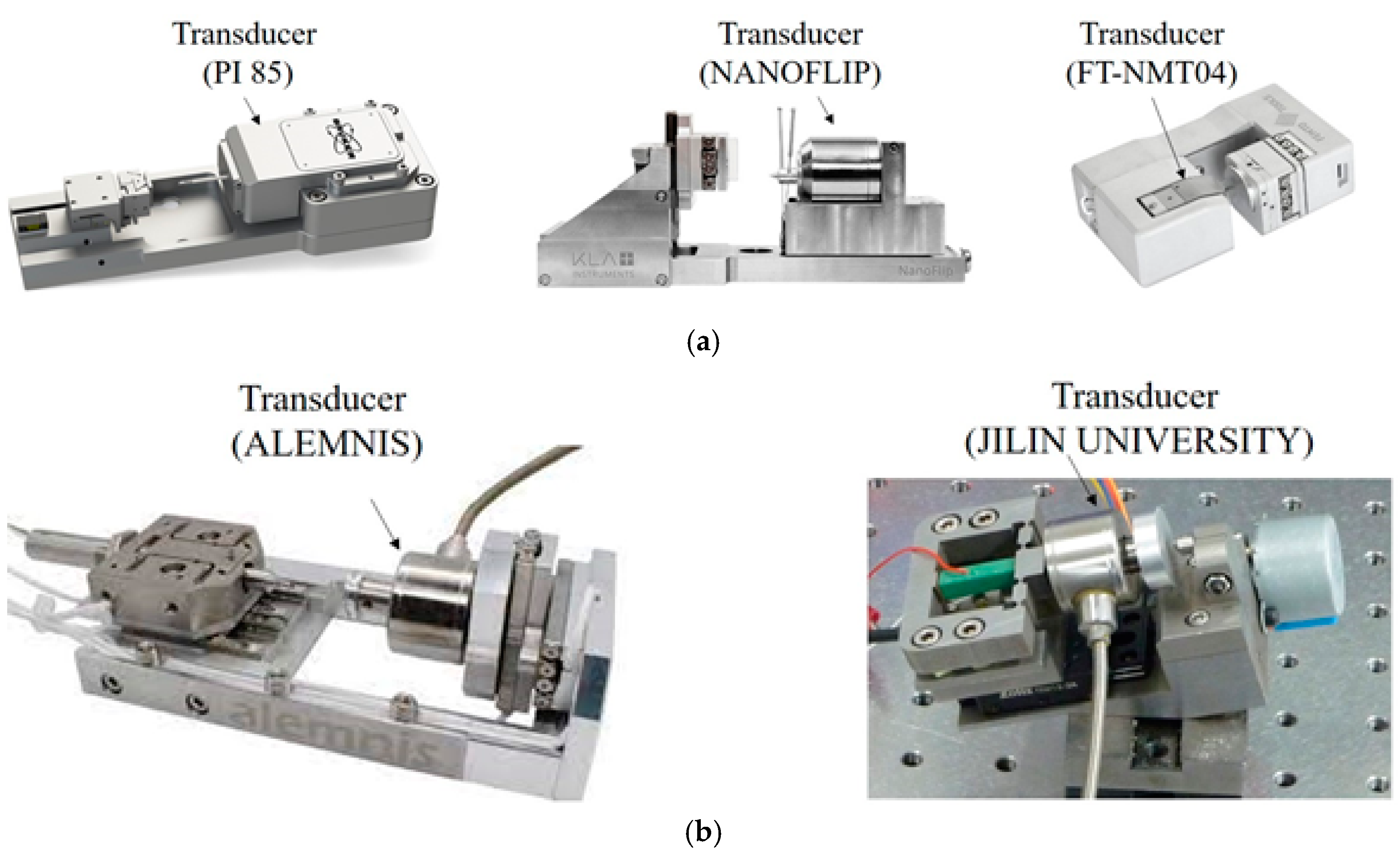
2. State-of-the-Art
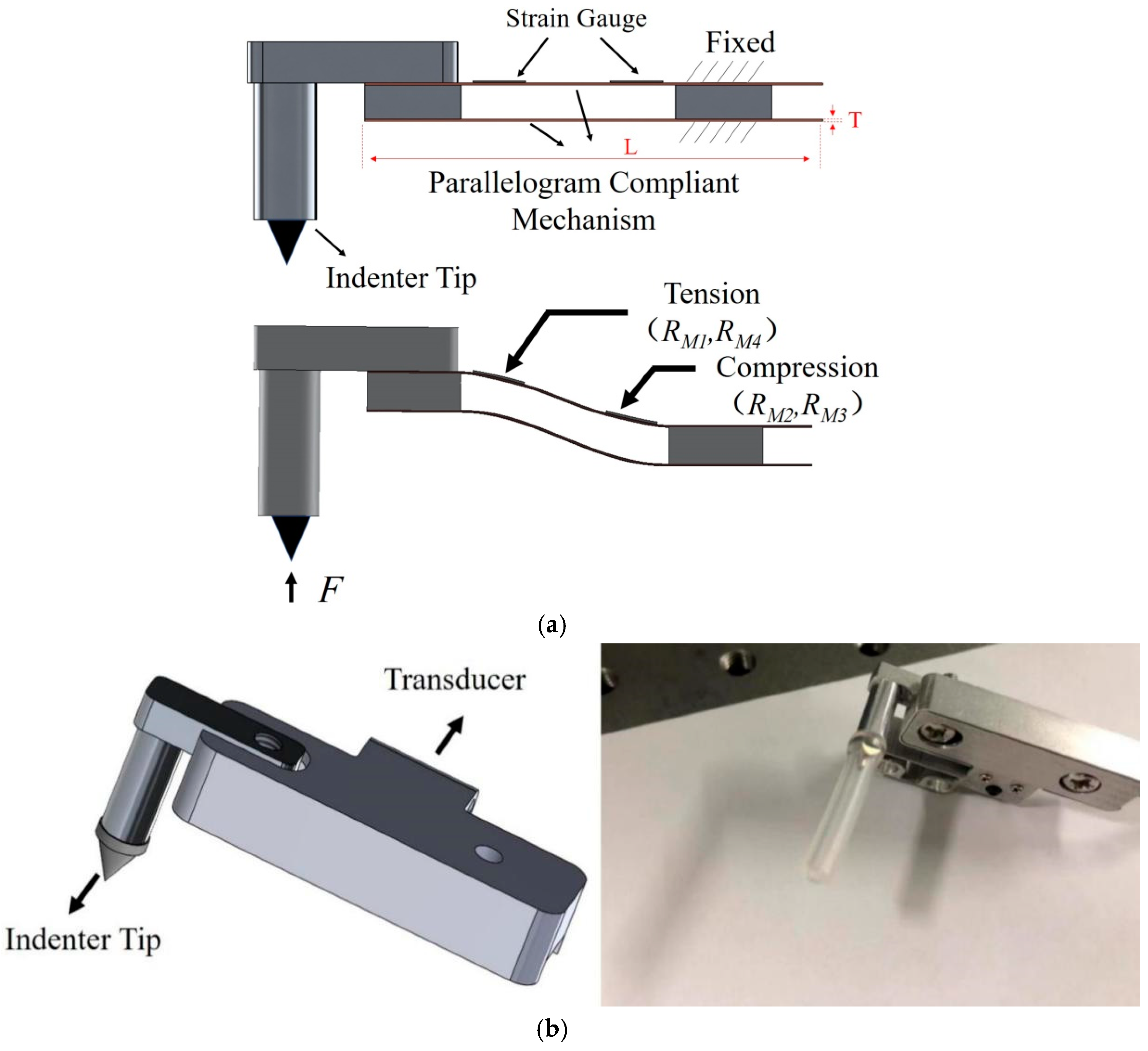
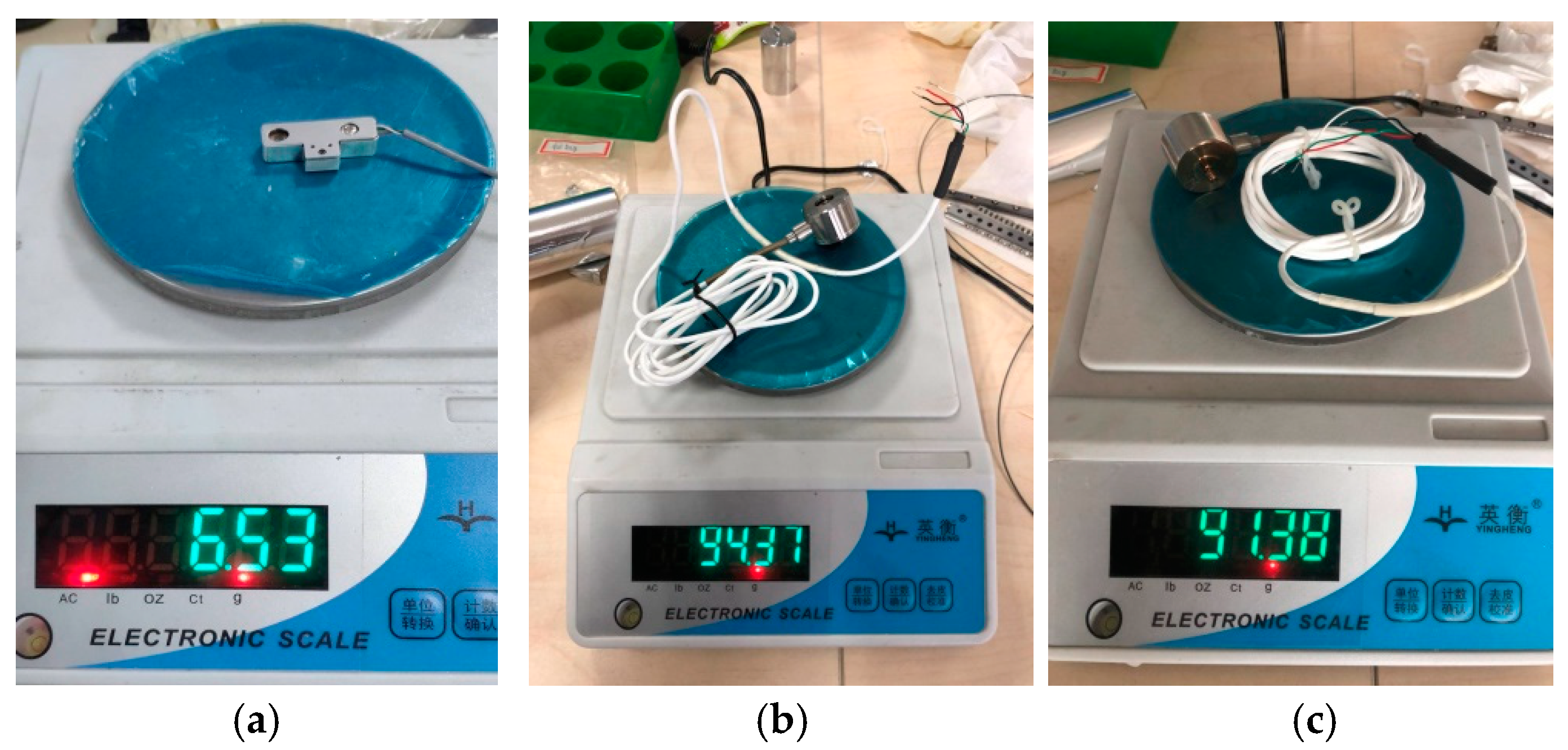
3. Transducer Design
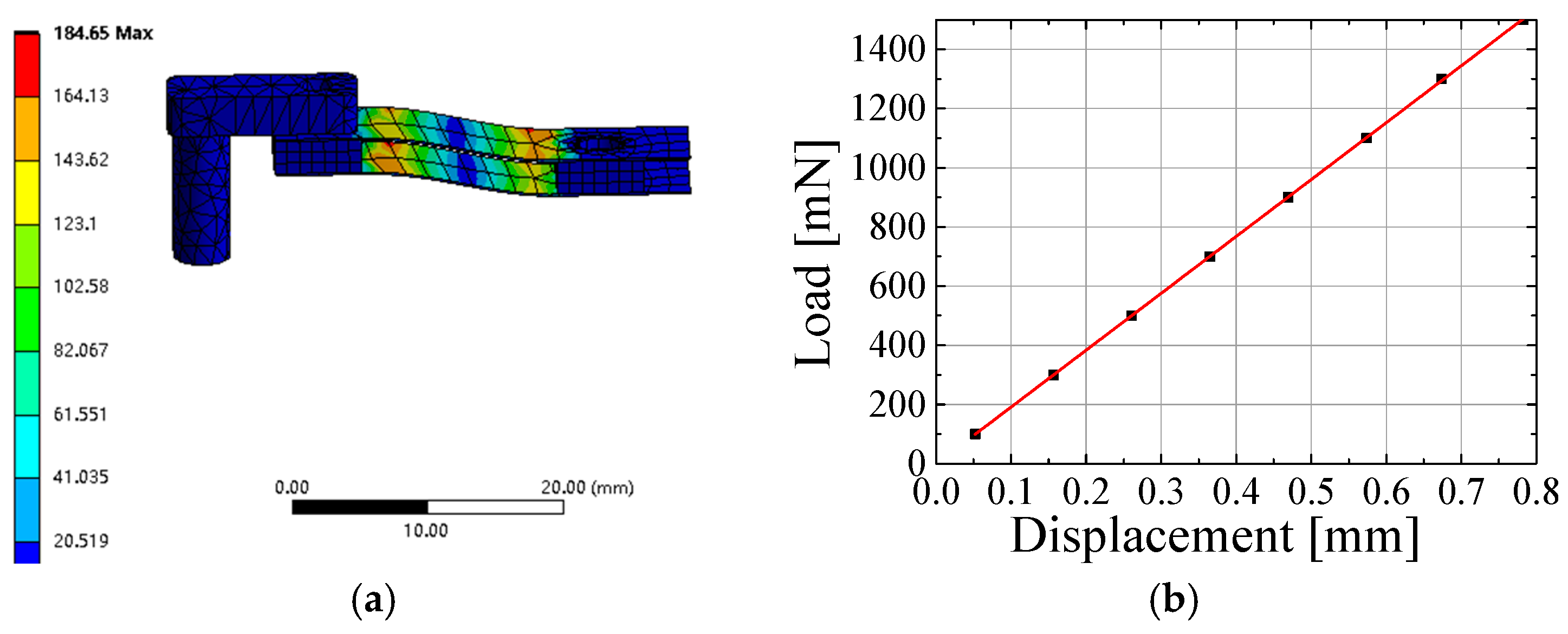
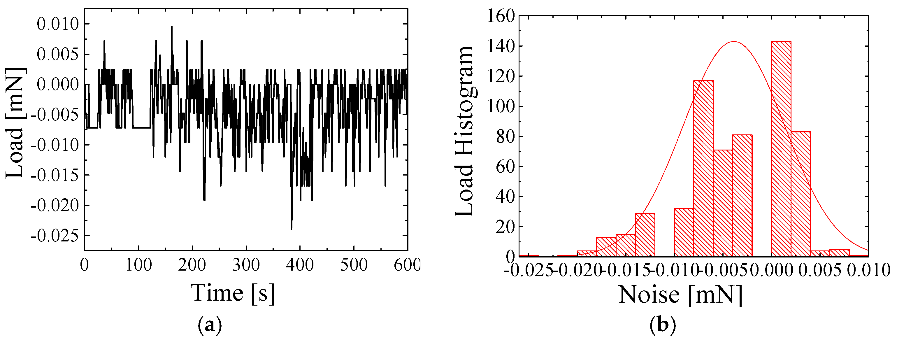
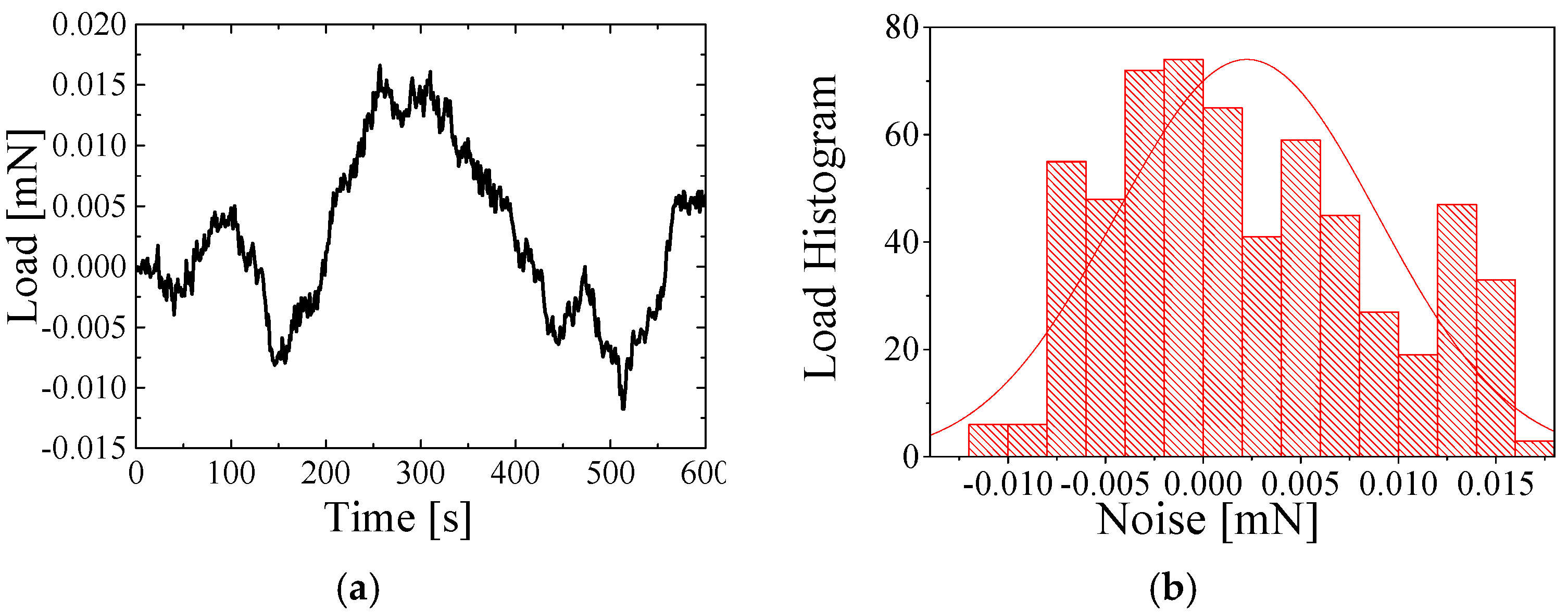
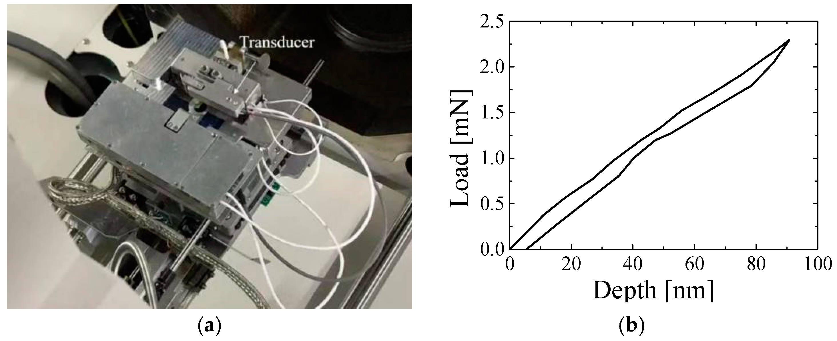
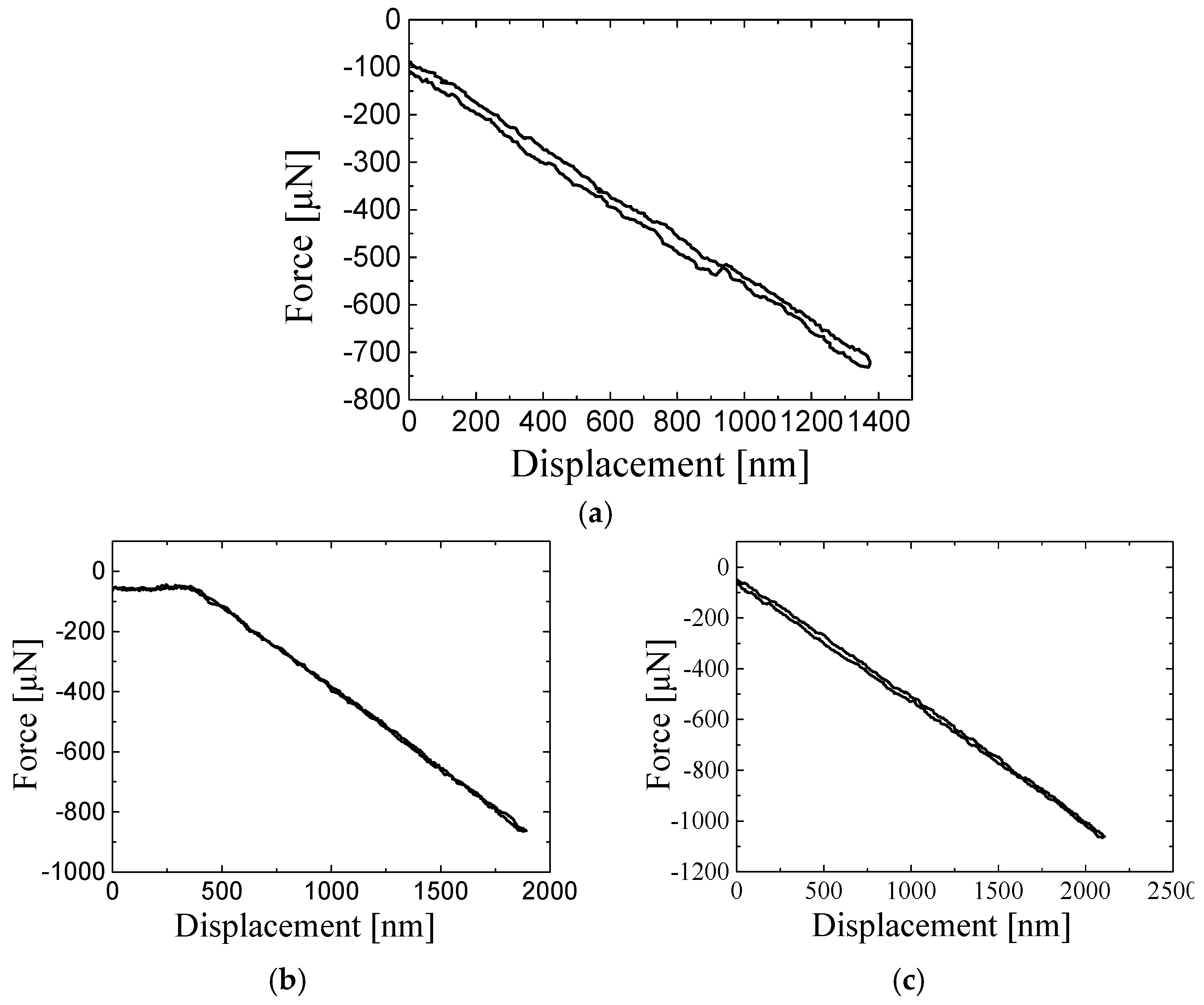
4. Results
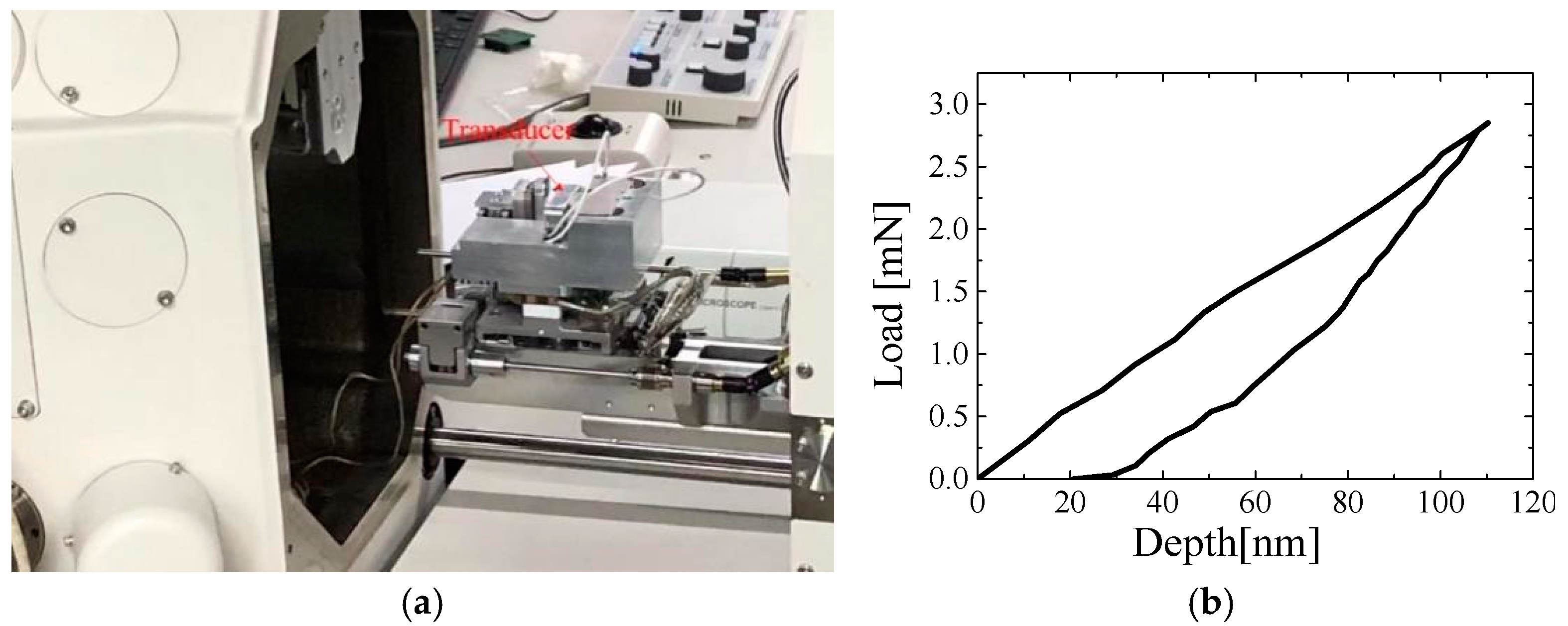
5. Application
6. Conclusions
Author Contributions
Funding
Institutional Review Board Statement
Informed Consent Statement
Data Availability Statement
Conflicts of Interest
References
- Guo, H.; Wang, M.; Liu, J.; Zhu, S.; Liu, C. Facile synthesis of nanoscale high porosity IR-MOFs for low-k dielectrics thin films. Microporous Mesoporous Mater. 2016, 221, 40–47. [Google Scholar] [CrossRef]
- Huang, D.; Li, L.; Wang, K.; Li, Y.; Feng, K.; Jiang, F. Wittichenite semiconductor of Cu3BiS3 films for efficient hydrogen evolution from solar driven photoelectrochemical water splitting. Nat. Commun. 2021, 12, 3795. [Google Scholar] [CrossRef] [PubMed]
- Vereschaka, A.; Tabakov, V.; Grigoriev, S.; Sitnikov, N.; Milovich, F.; Andreev, N.; Sotova, C.; Kutina, N. Investigation of the Influ-ence of the Thickness of Nanolayers in Wear-resistant Layers of Ti-TiN-(Ti,Cr,Al)N Coating on Destruction in the Cutting and Wear of Carbide Cutting Tools. Surf. Coat. Technol. 2020, 385, 125402. [Google Scholar] [CrossRef]
- Bobzin, K.; Brögelmann, T.; Kruppe, N.C.; Carlet, M. Wear behavior and thermal stability of HPPMS (Al,Ti,Cr,Si)ON, (Al,Ti,Cr,Si)N and (Ti,Al,Cr,Si)N coatings for cutting tools. Surf. Coat. Technol. 2020, 385, 125370. [Google Scholar] [CrossRef]
- Rahman, F.; Ngaile, G.; Hassan, T. Development of scanning electron microscope-compatible multiaxial miniature testing system. Meas. Sci. Technol. 2019, 30, 105902. [Google Scholar] [CrossRef]
- Zhang, D. A Nano-Tensile Testing System for Studying Nanostructures Inside an Electron Microscope: Design, Characterization and Application. THESIS. EPFL, 2010. Available online: https://infoscience.epfl.ch/entities/publication/add1ef7e-c7fb-4abb-bf87-46743a6a17d8 (accessed on 14 January 2025).
- Barnoush, A.; Hosemann, P.; Molina-Aldareguia, J.; Wheeler, J.M. In situ small-scale mechanical testing under extreme environments. Bulletin 2019, 44, 471–477. [Google Scholar] [CrossRef]
- Herrmann, K.; Hasche, K.; Pohlenz, F.; Seemann, R. Characterisation of the geometry of indenters used for the micro- and nanoindentation method. Measurement 2021, 29, 201–207. [Google Scholar] [CrossRef]
- Du, D.; Wu, Y.; Zhao, Y.; Lu, M.; Huang, H. Deformation and fracture behaviours of a YAG single crystal characterized using nanoindentation method. Mater. Charact. 2020, 164, 110302. [Google Scholar] [CrossRef]
- Sutton, M.A.; Li, N.; Garcia, D.; Cornille, N.; Orteu, J.J.; McNeill, S.R.; Schreier, H.W.; Li, X. Metrology in a Scanning Electron Microscope: Theoretical Developments and Experimental Validation. Meas. Sci. Technol. 2006, 17, 2613. [Google Scholar] [CrossRef]
- Wheeler, J.M.; Michler, J. Invited Review Article: Large ring lasers for rotation sensing. Rev. Sci. Instrum. 2013, 84, 041101. [Google Scholar]
- Raju, T.D.; Nakasa, K.; Kato, M. Relation between delamination of thin flims and backward deviation of load–displacement curves under repeating nanoindentation. Acta Mater. 2003, 51, 457–467. [Google Scholar] [CrossRef]
- Williams, J.J.; Chapman, N.C.; Chawla, N. Mechanisms of Sn hillock growth in vacuum by in situ nanoindentation in a scanning electron microscope (SEM). J. Electron. Mater. 2013, 42, 224–229. [Google Scholar] [CrossRef]
- Ast, J.; Mohanty, G.; Guo, Y.; Michler, J.; Maeder, X. In situ micromechanical testing of tungsten micro-cantilevers using HR-EBSD for the assessment of deformation evolution. Mater. Des. 2017, 117, 265–266. [Google Scholar] [CrossRef]
- Jun, T.-S.; Zhang, Z.; Sernicola, G.; Dunne, F.P.E.; Britton, T.B. Local strain rate sensitivity of single α phase within a dual-phase Ti alloy. Acta Mater. 2016, 107, 298–309. [Google Scholar] [CrossRef]
- Jo, Y.H.; Choi, W.-M.; Sohn, S.S.; Kim, H.S.; Lee, B.-J.; Lee, S. Role of brittle sigma phase in cryogenic-temperature-strength improvement of non-equi-atomic Fe-rich VCrMnFeCoNi high entropy alloys. Mater. Sci. Eng. A 2018, 724, 403–410. [Google Scholar] [CrossRef]
- Lentz, J.; Röttger, A.; Theisen, W. Hardness and modulus of Fe2B, Fe3(C,B), and Fe23(C,B)6 borides and carboborides in the Fe-C-B system. Mater. Charact. 2018, 135, 192–202. [Google Scholar] [CrossRef]
- Gao, Z.; Buchinger, J.; Koutná, N.; Wojcik, T.; Hahn, R.; Mayrhofer, P.H. Ab initio supported development of TiN/MoN superlattice thin films with improved hardness and toughness. Acta Mater. 2022, 231, 117871. [Google Scholar] [CrossRef]
- Guo, Y.; Schwiedrzik, J.; Michler, J.; Maeder, X. On the nucleation and growth of {1122} twin in commercial purity titanium: In situ investigation of the local stress field and dislocation density distribution. Acta Mater. 2016, 120, 292–301. [Google Scholar] [CrossRef]
- Zhao, H.; Huang, H.; Fan, Z.; Yang, Z.; Ma, Z. Nanoindentation in Materials Science; IntechOpen: London, UK, 2012. [Google Scholar]
- ISO (2023). ISO 5725 Accuracy (Trueness and Precision) of Measurement Methods and Results—Part 1: General Principles and Definitions. Available online: https://cdn.standards.iteh.ai/samples/69418/a7c3fb78cdce4a6398bd3f759670d72e/ISO-5725-1-2023.pdf (accessed on 14 January 2025).


| Thickness (mm) | 0.05 | 0.1 | 0.15 | 0.2 | 0.25 | 0.3 |
|---|---|---|---|---|---|---|
| Simulated | 1.2058 × 10⁻⁴ | 3.0131 × 10⁻⁵ | 1.346 × 10⁻⁵ | 7.6476 × 10⁻⁶ | 4.946 × 10⁻⁶ | 3.4707 × 10⁻⁶ |
| Calculated | 1.173913 × 10⁻⁴ | 2.93478 × 10⁻⁵ | 1.30434 × 10⁻⁵ | 7.33695 × 10⁻⁶ | 4.69565 × 10⁻⁶ | 3.26086 × 10⁻⁶ |
| Relative error (%) | 2.6 | 2.6 | 3.1 | 4.1 | 5.1 | 6.1 |
Disclaimer/Publisher’s Note: The statements, opinions and data contained in all publications are solely those of the individual author(s) and contributor(s) and not of MDPI and/or the editor(s). MDPI and/or the editor(s) disclaim responsibility for any injury to people or property resulting from any ideas, methods, instructions or products referred to in the content. |
© 2025 by the authors. Licensee MDPI, Basel, Switzerland. This article is an open access article distributed under the terms and conditions of the Creative Commons Attribution (CC BY) license (https://creativecommons.org/licenses/by/4.0/).
Share and Cite
Lu, D.; Liu, J.; Wang, M.; Gu, S. State-of-the-Art Design and Optimization of Strain Gauge-Type Load–Displacement Transducer for in In Situ Nanoindentation Systems. Sensors 2025, 25, 609. https://doi.org/10.3390/s25030609
Lu D, Liu J, Wang M, Gu S. State-of-the-Art Design and Optimization of Strain Gauge-Type Load–Displacement Transducer for in In Situ Nanoindentation Systems. Sensors. 2025; 25(3):609. https://doi.org/10.3390/s25030609
Chicago/Turabian StyleLu, Duhui, Jianliang Liu, Mukai Wang, and Sen Gu. 2025. "State-of-the-Art Design and Optimization of Strain Gauge-Type Load–Displacement Transducer for in In Situ Nanoindentation Systems" Sensors 25, no. 3: 609. https://doi.org/10.3390/s25030609
APA StyleLu, D., Liu, J., Wang, M., & Gu, S. (2025). State-of-the-Art Design and Optimization of Strain Gauge-Type Load–Displacement Transducer for in In Situ Nanoindentation Systems. Sensors, 25(3), 609. https://doi.org/10.3390/s25030609