
Design of Microstrip Antenna Integrating 24 GHz and 77 GHz Compact High-Gain Arrays

Abstract
1. Introduction
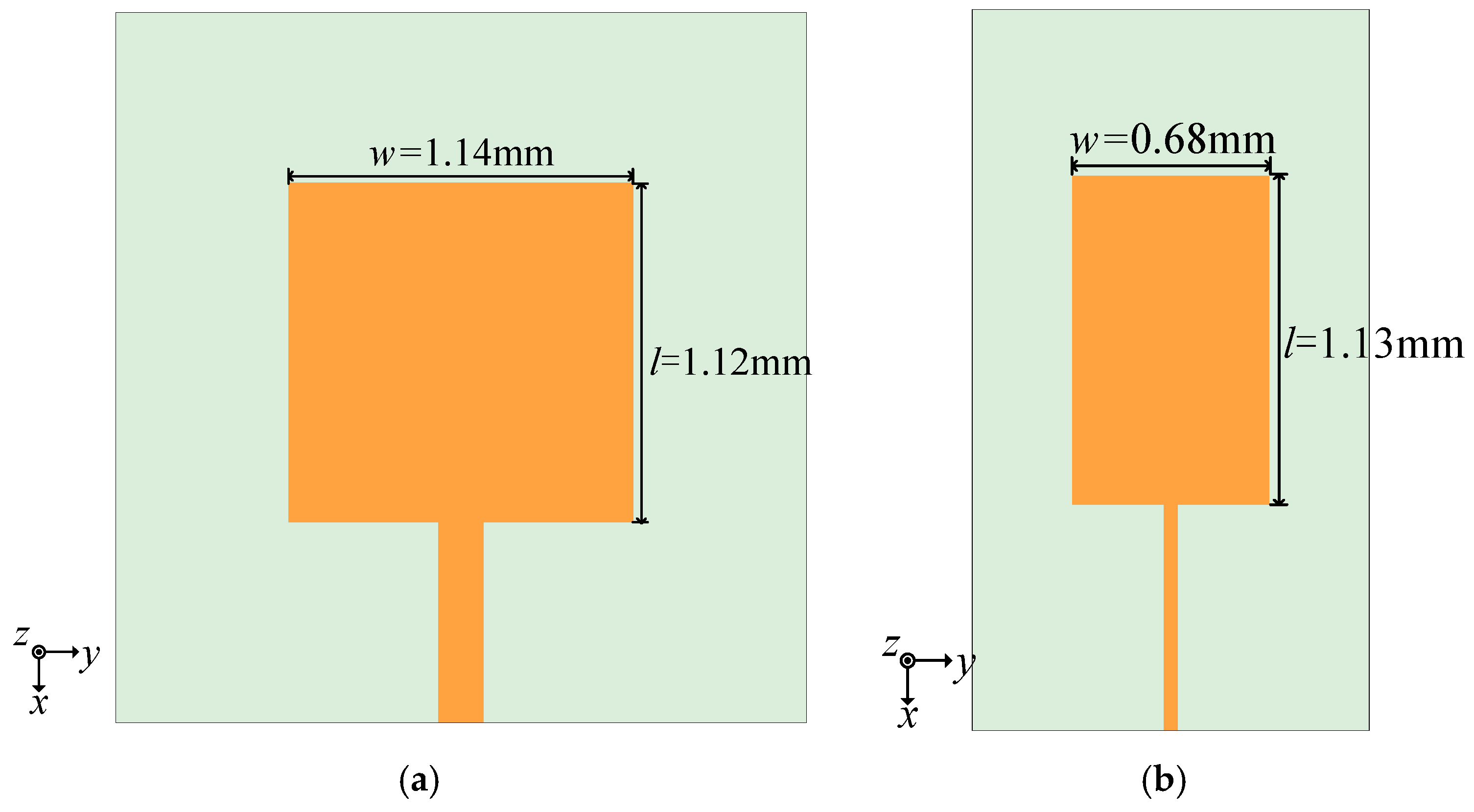
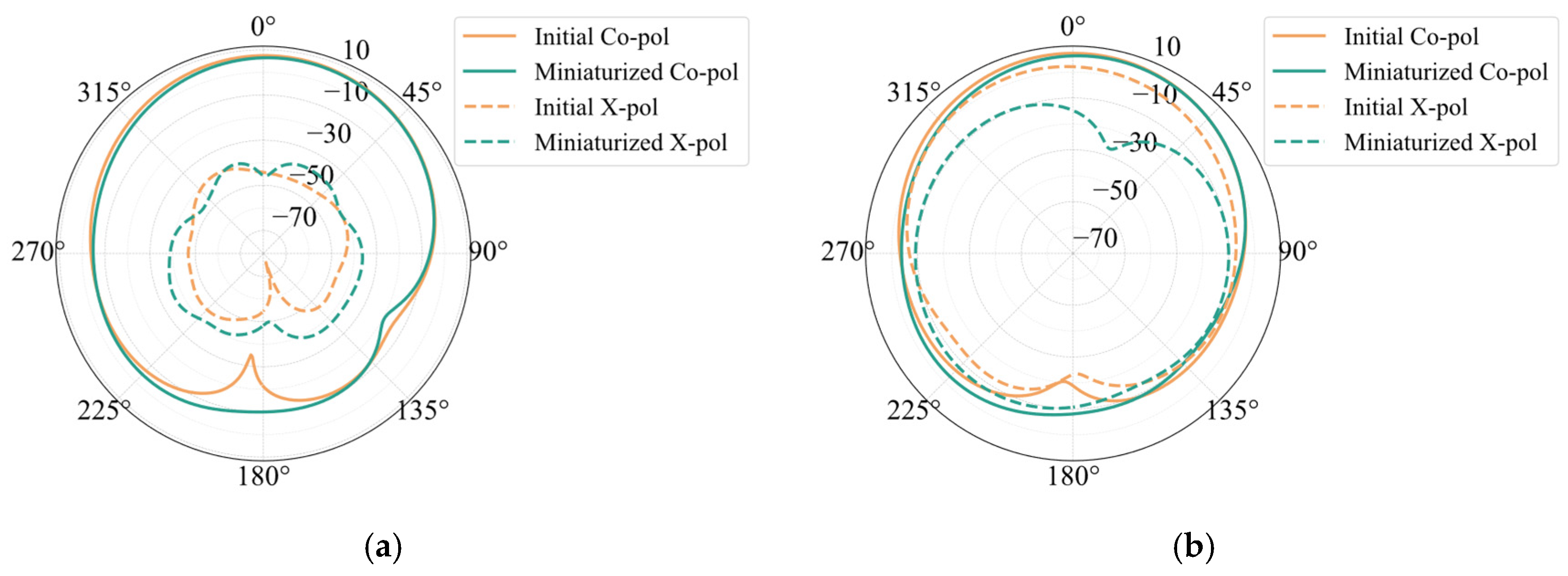
2. Antenna Unit
- Calculate the patch width: .
- Calculate the equivalent dielectric constant of the patch: .
- Calculate the extension length of the patch : .
- Calculate the length of the patch: .
3. Array Antenna Structure
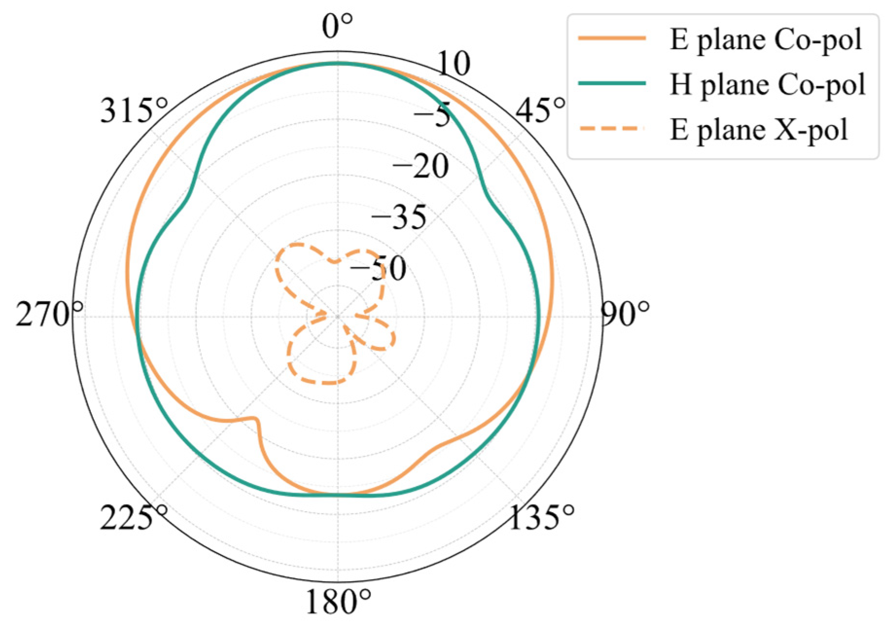
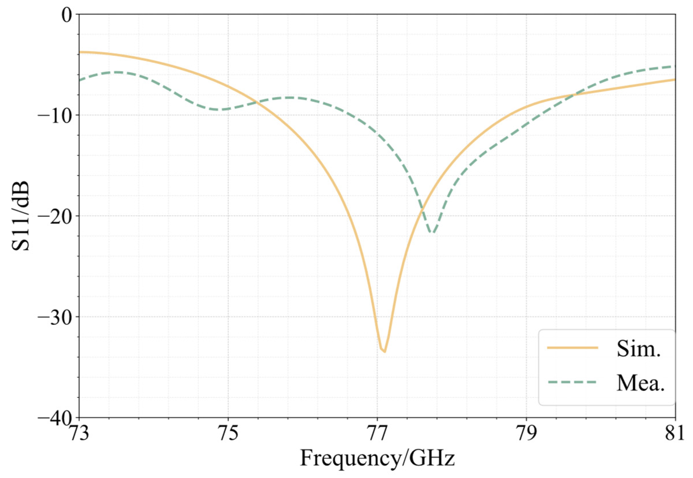
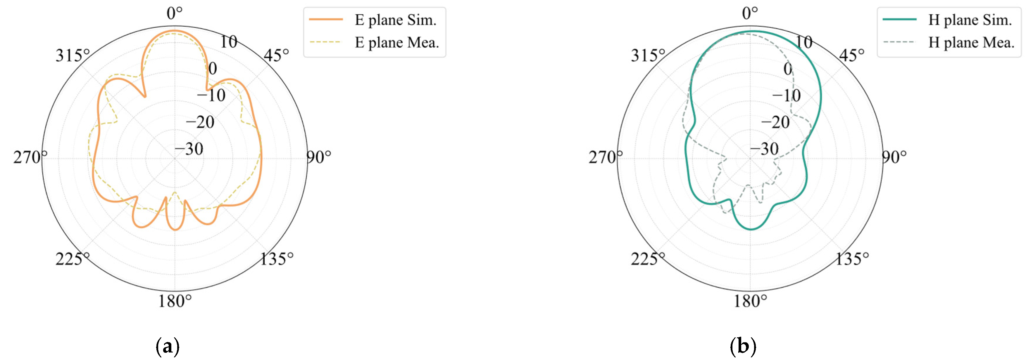
3.1. The 77 GHz Antenna Array
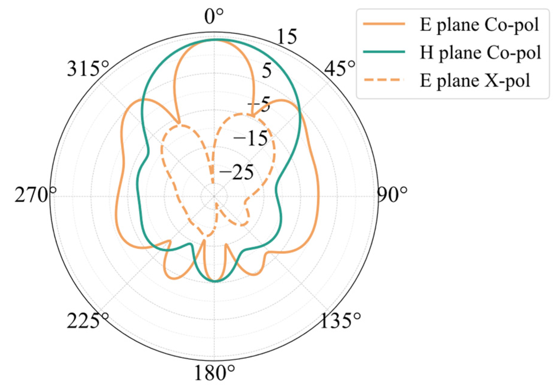
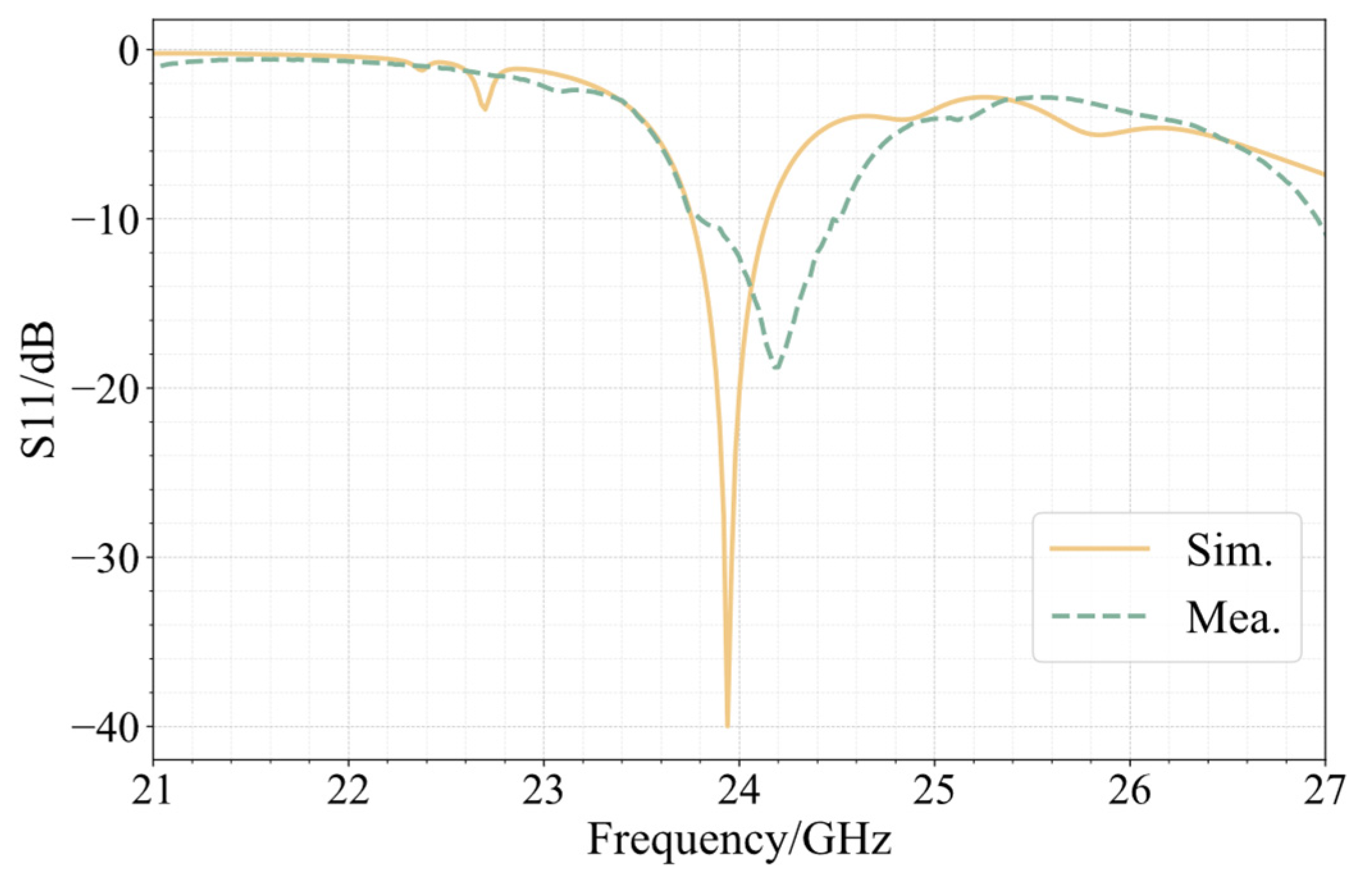
3.2. The 24 GHz Antenna Array
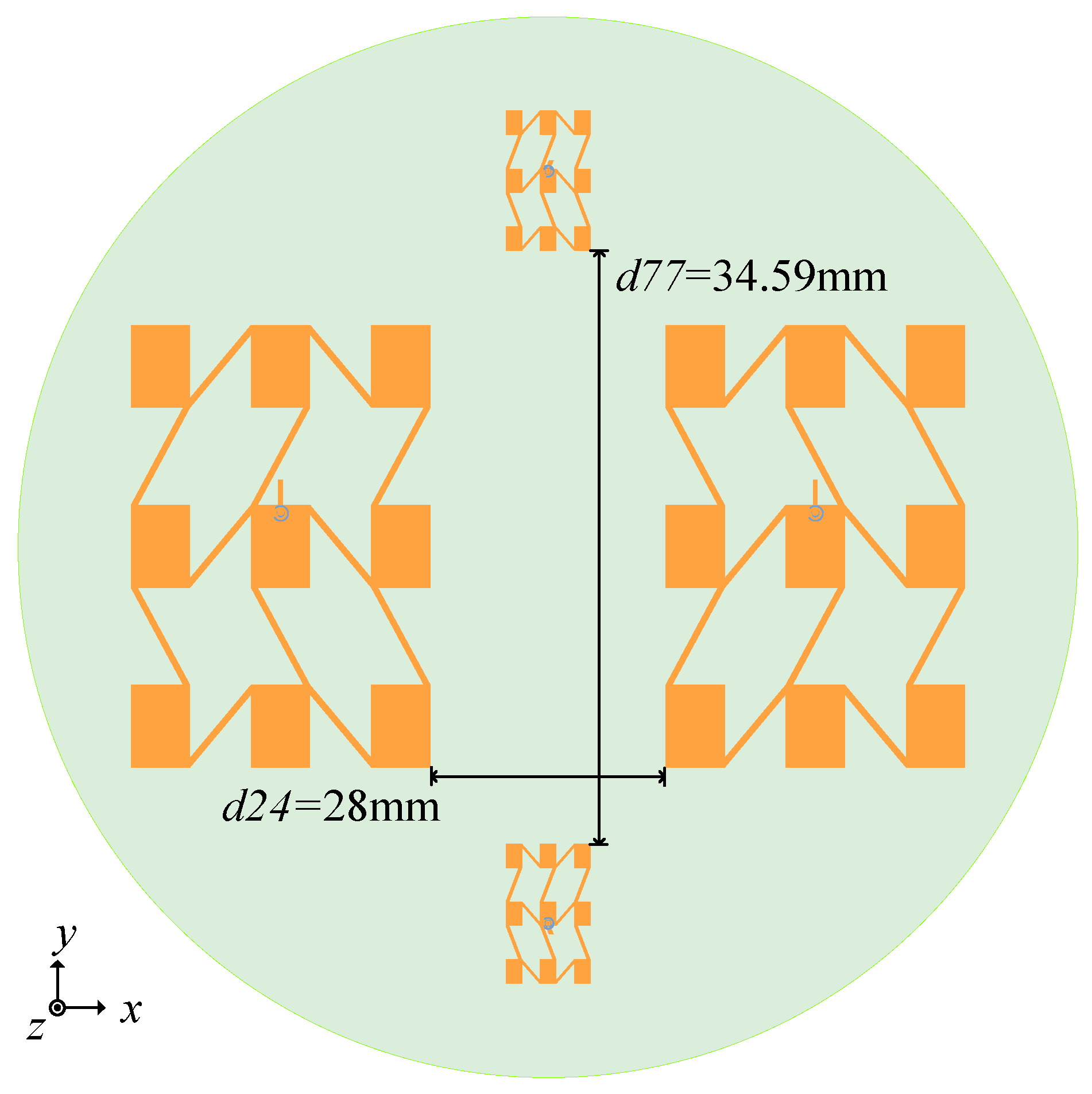
3.3. Integrated Array
4. Conclusions
Author Contributions
Funding
Institutional Review Board Statement
Informed Consent Statement
Data Availability Statement
Conflicts of Interest
References
- Waterhouse, R.B. Small Microstrip Patch Antennas. In Microstrip Patch Antennas: A Designer’s Guide; Springer: Boston, MA, USA, 2003; pp. 197–276. [Google Scholar] [CrossRef]
- Kumar, S.; Vishwakarma, D.K. Miniaturized Curved Slotted Patch Antenna over a Fractalized EBG Ground Plane. Int. J. Microw. Wirel. Technol. 2017, 9, 599–605. [Google Scholar] [CrossRef]
- Mohamad Isa, M.S.; Awang Md Isa, A.; Mohd Zin, M.S.I.; Mohd Johar, F.; Zakaria, Z. Microstrip Patch Antenna Array Mutual Coupling Reduction Using Capacitive Loaded Miniaturized EBG. J. Telecommun. Electron. Comput. Eng. 2012, 4, 27–34. [Google Scholar]
- Zhang, B.; Xu, X. Design of a Miniaturized Annular Ring Metamaterial Microstrip Antenna. In Proceedings of the 2021 International Symposium on Antennas and Propagation (ISAP), Taipei, Taiwan, 19–22 October 2021; pp. 1–2. [Google Scholar] [CrossRef]
- Tiwari, D.; Ansari, J.A.; Saroj, A.K.; Kumar, M. Analysis of a Miniaturized Hexagonal Sierpinski Gasket Fractal Microstrip Antenna for Modern Wireless Communications. AEU—Int. J. Electron. Commun. 2020, 123, 153288. [Google Scholar] [CrossRef]
- Gupta, M.; Mathur, V.; Kumar, A.; Saxena, V.; Bhatnagar, D. Microstrip Hexagonal Fractal Antenna for Military Applications. Frequenz 2019, 73, 321–330. [Google Scholar] [CrossRef]
- Kansal, S.; Singh, S. Design and Analysis of Dual-Reverse-Arrow Fractal Geometry Based Miniaturized Thin Strip Patch Antenna for Ultra-Wideband Applications. Int. J. Adv. Res. Comput. Sci. 2017, 8, 213–218. [Google Scholar]
- Gagnon, A.; Eroglu, A. Multilayer Coupler Design and Implementation for RFID Systems and Energy Harvesting Applications. In Proceedings of the 2016 IEEE/ACES International Conference on Wireless Information Technology and Systems (ICWITS) and Applied Computational Electromagnetics (ACES), Honolulu, HI, USA, 13–18 March 2016; IEEE: Piscataway, NJ, USA, 2016; pp. 1–2. [Google Scholar] [CrossRef]
- Sugadev, M.; Logashanmugam, E. A Compact Multiple Slot Microstrip Antenna for Modern Mobile Communications. In Proceedings of the 2016 International Conference on Control, Instrumentation, Communication and Computational Technologies (ICCICCT), Kumaracoil, India, 16–17 December 2016; IEEE: Piscataway, NJ, USA, 2016; pp. 805–808. [Google Scholar] [CrossRef]
- Zhu, J.; Sun, C.; Chen, M.; Liu, J. Design of Miniaturized Wideband Beam Deflection Conformal Array Antenna. Sensors 2023, 23, 930. [Google Scholar] [CrossRef]
- Pandey, U.; Singh, P.; Singh, R.; Gupta, N.P.; Arora, S.K.; Nizeyimana, E. Miniaturized Ultrawideband Microstrip Antenna for IoT-Based Wireless Body Area Network Applications. Wirel. Commun. Mob. Comput. 2023, 2023, e3950769. [Google Scholar] [CrossRef]
- Biradar, N.; Chandra, K.S. Modeling of Miniaturized Microstrip Patch Antenna Having Concentric Polygon Shaped with Eight Segments Slots Based on DGS for Multiband Wireless Applications Using Parametric Analysis. Des. Eng. 2022, 1, 610–621. [Google Scholar]
- Ajay, V.G.; Parvathy, A.R.; Mathew, T. Microstrip Antenna with DGS Based on CSRR Array for WiMAX Applications. Int. J. Electr. Comput. Eng. (IJECE) 2019, 9, 157–162. [Google Scholar] [CrossRef]
- Yu, Y.; Wang, Y.; Wang, R. Miniaturized Printed Antenna with Dual Inductor-Loaded Monopoles for Mobile Terminals. In Proceedings of the 2016 IEEE MTT-S International Wireless Symposium (IWS), Shanghai, China, 14–16 March 2016; IEEE: Piscataway, NJ, USA, 2016; pp. 1–3. [Google Scholar] [CrossRef]
- Bhuvaneswari, H.B.; Konnur, A.C.; Vadeyanpur, S.K. High Gain Patch Antenna Using EBG Structures for WiMAX Application. IOP Conf. Ser. Mater. Sci. Eng. 2021, 1070, 012073. [Google Scholar] [CrossRef]
- Abdulhameed, M.K.; Isa, M.S.M.; Zakaria, Z.; Mohsin, M.K.; Attiah, M.L. Mushroom-Like EBG to Improve Patch Antenna Performance for C-Band Satellite Application. Int. J. Electr. Comput. Eng. (IJECE) 2018, 8, 3875–3881. [Google Scholar] [CrossRef]
- Deng, F.; Qi, J. Shrinking Profile of Fabry–Perot Cavity Antennas With Stratified Metasurfaces: Accurate Equivalent Circuit Design and Broadband High-Gain Performance. IEEE Antennas Wirel. Propag. Lett. 2020, 19, 208–212. [Google Scholar] [CrossRef]
- Meriche, M.A.; Attia, H.; Messai, A.; Mitu, S.S.I.; Denidni, T.A. Directive Wideband Cavity Antenna With Single-Layer Meta-Superstrate. IEEE Antennas Wirel. Propag. Lett. 2019, 18, 1771–1774. [Google Scholar] [CrossRef]
- Chatterjee, D.; Kundu, A.K. High Gain Metamaterial Antenna Using Linear Displacement of SRR Elements. Texa. J. Mutl. Stud. 2021, 2, 77–84. [Google Scholar]
- Le, M.T.; Nguyen, Q.C.; Vuong, T.P. Design of High-Gain and Beam Steering Antennas Using a New Planar Folded-Line Metamaterial Structure. Int. J. Antennas Propag. 2014, 2014, e302580. [Google Scholar] [CrossRef]
- Fu, C.; Feng, C.; Chu, W.; Yue, Y.; Zhu, X.; Gu, W. Design of a Broadband High-Gain Omnidirectional Antenna With Low Cross Polarization Based on Characteristic Mode Theory. IEEE Antenn. Wirel. Propag. 2022, 21, 1747–1751. [Google Scholar] [CrossRef]
- Saeed, M.A.; Obi, E.R.; Nwajana, A.O. A Compact Linear Microstrip Patch Beamformer Antenna Array for Millimeter-Wave Future Communication. Sensors 2024, 24, 4068. [Google Scholar] [CrossRef] [PubMed]
- Didi, S.-E.; Halkhams, I.; Es-Saqy, A.; Fattah, M.; Balboul, Y.; Mazer, S.; Bekkali, M.E. New Microstrip Patch Antenna Array Design at 28 GHz Millimeter-Wave for Fifth-Generation Application. Int. J. Electr. Comput. Eng. (IJECE) 2023, 13, 4184–4193. [Google Scholar] [CrossRef]
- Kunooru, B.; Nandigama, S.V.; RamaKrishna, D.; Gugulothu, R. Design and Analysis of a Microstrip Antenna Array for High Gain Applications at Mm Wave Frequencies. In Proceedings of the 2019 TEQIP III Sponsored International Conference on Microwave Integrated Circuits, Photonics and Wireless Networks (IMICPW), Tiruchirappalli, India, 22–24 May 2019; pp. 233–237. [Google Scholar] [CrossRef]
- Phalak, K.; Sebak, A. Aperture Coupled Microstrip Patch Antenna Array for High Gain at Millimeter Waves. In Proceedings of the 2014 IEEE International Conference on Communication, Networks and Satellite (COMNETSAT), Jakarta, Indonesia, 4–5 November 2014; pp. 13–16. [Google Scholar] [CrossRef]


| Antenna Type | Antenna Size (mm2) | Frequency (GHz) | Bandwidth (GHz) | Gain (dB) | Sidelobe Level (dB) | Cross-Polarization (dB) |
|---|---|---|---|---|---|---|
| Initial patch | 1.12 × 1.14 | 77 | 4.04 | 7.43 | - | −51.68 @ center feed −5.16 @ corner feed |
| Miniaturized patch | 1.13 × 0.68 | 77 | 3.18 | 6.61 | - | −52.16 dB @ center feed −20.03 @ corner feed |
| 1 × 3 linear array | 2.26 × 4.74 | 77 | 7.18 | 10.10 | −14.29 | −53.54 |
| 3 × 3 planar array | 7.72 × 4.74 | 77 | 3.15 | 14.19 | −9.14 | −29.26 |
| 3 × 3 planar array | 24.76 × 16.92 | 24 | 0.38 | 15.34 | −12.85 | −40.52 |
| Circular array Ref [21] | 23.78 × 23.78 | 7.95 | 6.3 | 8.4 | - | −25 |
| 1 × 6 linear array Ref [22] | 6 × 26 | 28.8 | 0.7 | 9.19 | −2 | - |
| 1 × 2 linear array Ref [23] | 9 × 10.3 | 9.42 | 1.43 | 9.42 | - | - |
| 1 × 4 linear array Ref [24] | 11.3 × 22.5 | 30 | 1.25 | 12.63 | −13.66 | −44.79 |
| 1 × 4 linear array Ref [25] | 31 × 10 | 28 | 1.29 | 13.5 | −14.5 | - |
Disclaimer/Publisher’s Note: The statements, opinions and data contained in all publications are solely those of the individual author(s) and contributor(s) and not of MDPI and/or the editor(s). MDPI and/or the editor(s) disclaim responsibility for any injury to people or property resulting from any ideas, methods, instructions or products referred to in the content. |
© 2025 by the authors. Licensee MDPI, Basel, Switzerland. This article is an open access article distributed under the terms and conditions of the Creative Commons Attribution (CC BY) license (https://creativecommons.org/licenses/by/4.0/).
Share and Cite
Zhu, J.; Liu, J. Design of Microstrip Antenna Integrating 24 GHz and 77 GHz Compact High-Gain Arrays. Sensors 2025, 25, 481. https://doi.org/10.3390/s25020481
Zhu J, Liu J. Design of Microstrip Antenna Integrating 24 GHz and 77 GHz Compact High-Gain Arrays. Sensors. 2025; 25(2):481. https://doi.org/10.3390/s25020481
Chicago/Turabian StyleZhu, Junli, and Jingping Liu. 2025. "Design of Microstrip Antenna Integrating 24 GHz and 77 GHz Compact High-Gain Arrays" Sensors 25, no. 2: 481. https://doi.org/10.3390/s25020481
APA StyleZhu, J., & Liu, J. (2025). Design of Microstrip Antenna Integrating 24 GHz and 77 GHz Compact High-Gain Arrays. Sensors, 25(2), 481. https://doi.org/10.3390/s25020481