1. Introduction
The field of piezoelectric energy harvesting has witnessed a surge in the development of interface circuits tailored to its unique requirements [
1,
2]. This area of research has garnered considerable interest thanks to the remarkable attributes it offers, including high power density, a wide voltage range, and seamless integration with IC technology. What sets these interface circuits apart is the striking contrast between the operational speeds of ICs and the rhythmic nature of mechanical vibrations. This incongruity presents an exceptional opportunity to incorporate nonlinear switching and control mechanisms into the interface circuits, thereby enhancing the extraction of power to unprecedented levels. By capitalizing on this disparity, researchers have been able to unlock the true potential of piezoelectric energy harvesting. In a piezoelectric energy-harvesting system, the input power processing circuit plays a vital role in optimizing harvested energy. Comprising the interface and harvester control, this circuit ensures compatibility with the energy storage system. Due to the AC nature of piezoelectric vibrations, an AC-to-DC rectifier is used, posing challenges in efficient power extraction. Designing rectifier circuits that effectively extract power while minimizing losses and optimizing efficiency is a task for researchers and engineers. The harvester control component enables the interface to adapt and optimize performance based on varying vibration characteristics, enhancing power extraction efficiency. By fine-tuning the interface circuit, maximum utilization of available energy can be achieved.
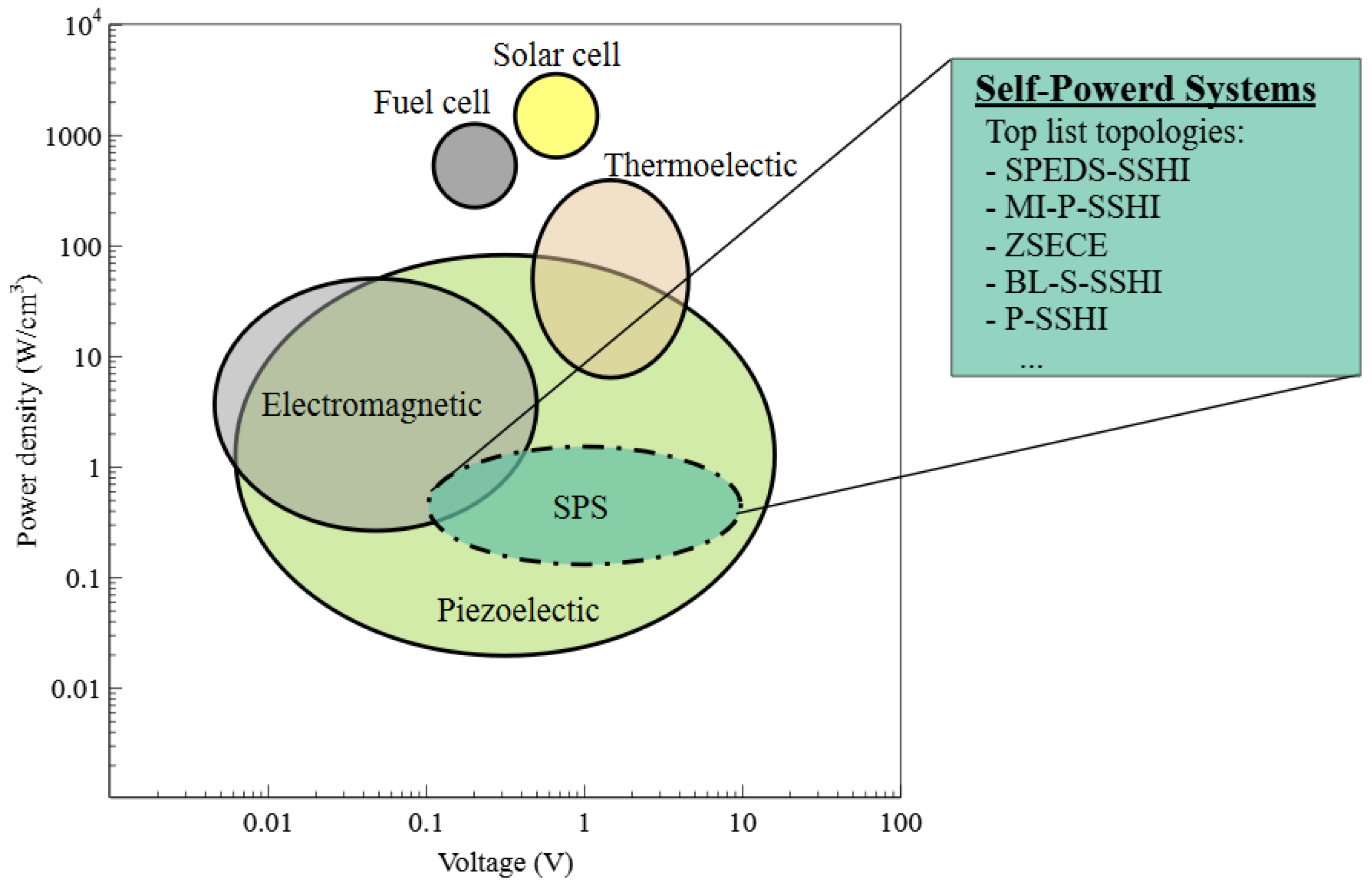
This section establishes the growing importance of piezoelectric energy harvesting and outlines the primary challenges in designing effective interface circuits by emphasizing the need for innovative circuit topologies that can reconcile the mismatch between mechanical vibrations and electronic processing speeds. It also highlights the potential benefits of a comparison that includes other energy harvesting techniques—such as solar, thermoelectric, or electromagnetic methods—to further contextualize the review’s scope and objectives as depicted in
Figure 1.
Researchers have made significant advancements in enhancing power extraction efficiency in piezoelectric energy harvesting systems by exploring nonlinear switching techniques. Two notable methods, synchronous electric charge extraction (SECE) and parallel synchronized switch harvesting on inductor (P-SSHI), have demonstrated promising results [
1,
3,
4,
5]. These techniques exploit synchronous switching at peak vibration displacement to unlock a substantial increase in extracted power. By introducing strategic timing delays in the switching process [
6,
7,
8], researchers have achieved complex impedance matching, enabling improved performance even at off-resonance frequencies. This innovation expands the operational range of the energy-harvesting system, ensuring efficient power extraction across a wider spectrum of vibration frequencies.
Furthermore, the development of interfaces incorporating multiple transducers has contributed to further advancements in power extraction [
9,
10]. By harnessing the collective energy from multiple transducers, these interfaces significantly enhance overall power output. This approach proves particularly beneficial in scenarios where a single transducer may not generate sufficient power independently. The combination of multiple transducers with sophisticated interface designs maximizes power extraction efficiency and facilitates practical implementation of piezoelectric energy harvesting systems. The integration of nonlinear switching techniques, timing delays, complex impedance matching, and the utilization of multiple transducers opens up new possibilities for enhancing power extraction efficiency in piezoelectric energy harvesting systems, leading to independent SPSs. These innovations pave the way for more efficient and practical utilization of piezoelectric energy in various applications. Optimizing interface circuits in piezoelectric energy harvesting systems requires careful parameter adjustments, regardless of the circuit architecture. The extracted power is influenced by the effective loading on the transducer. To address this, many designs incorporate a switching power converter after the rectifier, enabling adjustment of the effective loading through modifications in the converter’s switching timing [
11]. Start-up and runtime calibrations are crucial to maintain optimal performance in varying operating conditions.
Several maximum power point tracking (MPPT) algorithms have been proposed, including Perturb and Observe (P&O) and fractional
, each with tradeoffs in circuit complexity, tracking accuracy, convergence time, and power consumption [
12,
13]. This article introduces cutting-edge interface designs and MPPT methods for piezoelectric energy harvesting, emphasizing important considerations in circuit implementation. It provides valuable insights for optimizing circuit performance and achieving efficient power extraction from piezoelectric systems.
This paper systematically investigates the latest advancements in piezoelectric energy harvesting (PEH) systems and their interface circuits, addressing the inherent challenges of transforming mechanical vibrations into usable electrical energy by conducting a comprehensive literature review. To achieve this, a systematic analysis of interface circuits for self-powered piezoelectric energy harvesting was performed, employing comprehensive searches across academic databases including IEEE Xplore, MDPI, Scopus, Web of Science, and Google Scholar. This search strategy utilized a targeted approach, employing keywords and combinations such as ‘’piezoelectric energy harvesting”, ‘’self-powered systems”, ‘’interface circuit”, ‘’power management”, ‘’rectifier”, ‘’dc–dc converter”, ‘’MPPT”, ‘’SECE”, and ‘’SSH”. The review included peer-reviewed journal articles and conference proceedings focusing on interface circuit design, experimental validation, and self-powered system applications published between 2021 and 2025, ensuring the capture of the most relevant and recent contributions, while excluding purely theoretical studies or those solely focused on materials and fabrication without circuit analysis.
The article is organized as follows:
Section 2 lays out the fundamental principles of PEH and introduces the equivalent circuit model of a piezoelectric transducer. It discusses the challenges associated with AC-DC conversion, energy storage, voltage regulation, impedance matching, and the influence of load dependency on power extraction efficiency.
Section 3 examines basic interface circuits like full-bridge rectifiers (FBRs) and half-bridge rectifiers (HBRs), analyzing their advantages, limitations, and impact on energy harvesting efficiency.
Section 4 delves into advanced interface circuits, specifically Synchronous Switch Harvesting (SSH) techniques, which employ “switching manipulation” to optimize power extraction. It explores both open-circuit and short-circuit SSH interfaces, including Synchronous Electric Charge Extraction (SECE), predamping techniques (like S-SSHI), energy investing/pileup methods, and parallel SSHI (P-SSHI). The section discusses the principles, circuit topologies, control schemes, and performance improvements of these techniques. It also examines Maximum Power Point Tracking (MPPT) methods, such as fractional VOC and Perturb and Observe (P&O), for maximizing power extraction under varying load conditions. Additionally, it explores techniques for nonresonant operation, addressing challenges when the operating frequency deviates from the piezo structure’s resonant frequency.
Section 5 examines self-powered systems (SPSs) for PEH, categorizing them into single and array systems. For single SPSs, it discusses circuit implementations, efficiency, and power levels. For array SPSs, it looks into systems with multiple inputs, including thebenefits and challenges of using multiple transducers with different orientations, resonantfrequencies, and electrode configurations.
Section 6 provides a comparative analysis of the various interface circuits discussed in the previous sections, highlighting key features, advantages, and limitations. It discusses the importance of considering factors such as the number of switches, breakdown voltage limitations, calibration methods, power consumption, frequency deviations, and multi-input capabilities when selecting and designing interface circuits for specific PEH applications. The article concludes with a discussion of future research directions and the need for a holistic approach to optimize PEH systems, considering factors like environmental impact, power consumption, and real-world validation.
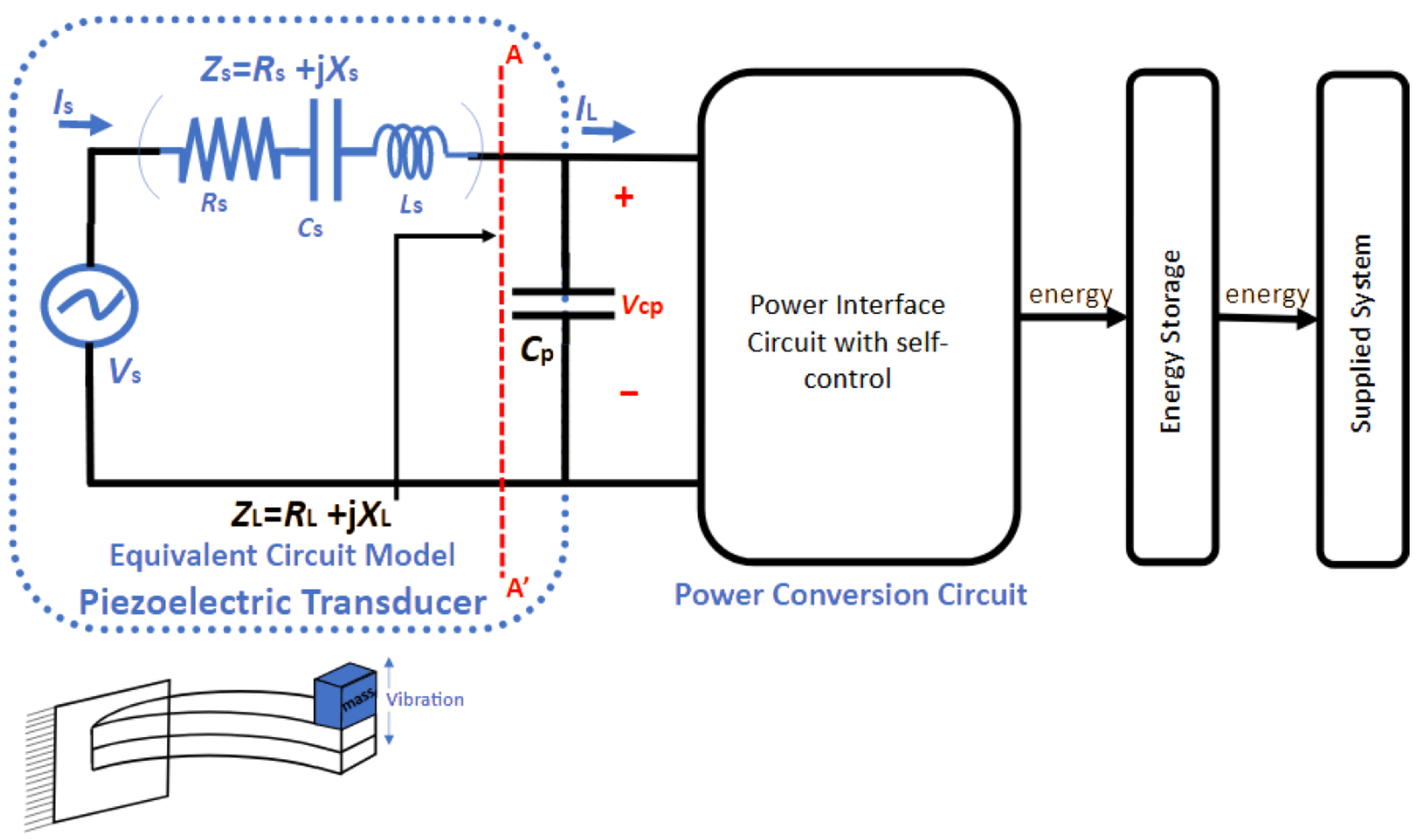
2. Equivalent Circuit Model
Piezoelectric materials have the remarkable ability to convert mechanical strain into electrical charges [
14]. One commonly used configuration for piezoelectric transducers is a cantilever beam with a mounted mass (
Figure 2). Shocks or vibrations applied to the system cause the attached mass to oscillate, generating strain in the piezoelectric material. By connecting the electrodes of the piezoelectric cantilever to a load through conductive wires, the generated charges form an electric current loop, enabling the transmission of power to the connected system. To gain a deeper understanding of this system’s behavior, a mathematical model is employed, considering the distinct densities of its components and assuming vibrations occur near the system’s resonant frequency. This model includes a mass, spring, damper, and the piezoelectric system itself [
15]. The governing equations of this model establish the interrelationships between parameters, providing a powerful tool for analyzing and predicting the system’s behavior. This mathematical framework empowers researchers and engineers to comprehend the underlying dynamics and optimize the performance of piezoelectric energy harvesting systems.
The piezoelectric transducer can be effectively represented by an equivalent circuit model using Equations (
1) and (
2), as illustrated in
Figure 2. The equation involves several parameters: mass (M), mechanical damping (
), stiffness (K), piezoelectric coefficient (
), and capacitance (
). The external force applied to the system is represented by F(t). This force can be a constant vibration (sinusoidal) or a sudden shock (impulsive). The system’s response includes the mass displacement (u(t)), voltage across the piezoelectric electrodes (
), and current flowing through them (
). This model incorporates parameters such as
=
,
=
,
=
, and
, which represent the equivalent resistance, inductance, and capacitances, respectively. The input voltage is denoted as
=
, and the electromechanical interface is depicted by the red line
A-
. The transducer structure exhibits two resonant frequencies: the open-circuit resonant frequency
and the short-circuit resonant frequency (
). These frequencies provide important insights into the resonant behavior of the transducer and play a crucial role in its performance analysis and optimization.
The equivalent circuit model section provides a detailed framework for understanding the piezoelectric transducer’s behavior. Key parameters—including mass, damping, stiffness, piezoelectric coefficient, and capacitance—are defined and related through governing equations. This summary underscores how these elements combine to form a model that is critical for predicting system performance and optimizing energy conversion.
The power processing circuit, depicted in
Figure 2, plays a crucial role in conditioning the extracted power for transfer to the connected system. This circuit performs AC-DC conversion, energy storage, and voltage regulation. It also determines the load seen by the transducer. According to the maximum power transfer (MPT) theorem, the power processing circuit, represented by impedance
, maximizes power transfer when it is a complex conjugate of the impedance on the other side of the electromechanical interface (
A-
). This condition, expressed as
[
14], ensures efficient power transfer. At maximum power transfer, the extracted power ideally matches the theoretical available power (
) given by
=
, where
is the force and
is the mechanical damping coefficient. However, in practical scenarios, the actual extracted power and electrical behavior are significantly influenced by the operations of the interface.
In recent years, significant progress has been made in enhancing the performance of interface circuits, mirroring the trends highlighted previously. Following the trends discussed in this article, which encompass various aspects of interface circuit enhancement, recent developments showcase advancements across several innovative circuit topologies. For example, the SPEDS-SSHI circuit in Qi et al. [
16] exemplifies progress in simultaneous energy harvesting from multiple PZTs and self-powered operation, achieving improved efficiency through component reuse, although practical validation requires further attention. Similarly, the Multi-input P-SSHI interface circuit in Wang et al. [
17] presents an efficient and simplified rectifier topology with self-powering capabilities, yet its scalability and robustness are areas for future investigation. Conversely, the Self-powered Extensible SECE Rectifier in Qiu et al. [
18] demonstrates load-independent power output and enhanced energy extraction, albeit with increased complexity and implementation costs. Furthermore, designs like the Self-powered Multi-Input Bridgeless series SSHI Circuit in Wu et al. [
19], leveraging voltage doubler topologies, achieve notable power increases but often lack comprehensive experimental details and face scalability challenges. Even optimized topologies such as the Self-Powered P-SSHI Circuit in Zouari et al. [
20], which enhance efficiency via transistor replacements, still present methodological gaps and validation needs. These diverse advancements, alongside emerging intelligent control strategies like AI-powered MPPT algorithms, underscore the continuous evolution toward more sophisticated interface circuit technology. However, these developments also emphasize the ongoing need for future research to address not only performance enhancement but also crucial practical considerations such as scalability, robust control methodologies, comprehensive experimental validation, and real-world applicability.
3. Basic Interface Circuits
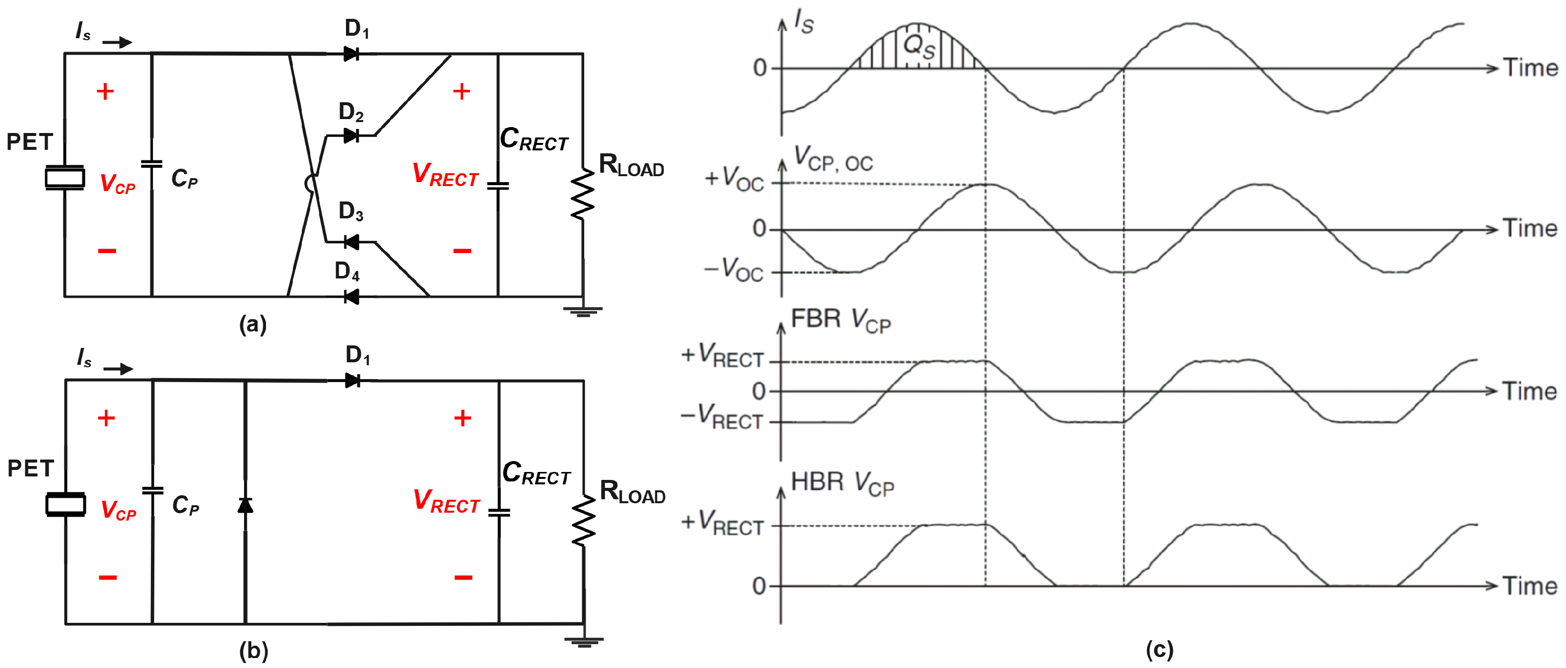
3.1. Full-Bridge Rectifiers
To convert the alternating current (AC) generated by a piezoelectric transducer into a direct current (DC) voltage suitable for application circuits, a rectifier is essential. A widely used and simple configuration is the full-bridge rectifier (FBR), as shown in
Figure 3. To maintain a stable voltage,
, during the quasi-steady state, a large capacitor,
, is connected at the rectifier’s output.
Figure 3 illustrates the waveforms of the interface current
, and the voltage across the piezoelectric electrodes,
, both with and without the rectifier. In the equivalent model depicted in
Figure 3, the interface current
is influenced by the operating frequency and the equivalent load,
. However, in practical situations where the real part of the load impedance
is much smaller than the real part of the source impedance (i.e., the internal impedance of the piezoelectric harvester), the system is far from impedance matching, and the extracted power is often significantly lower than the theoretically available power (
). This impedance mismatch can occur when the electromechanical coupling of the harvester is weak or when the harvester is operating far from its resonant frequency. Under these conditions, where the real part of
is negligible compared to the real part of the source impedance,
can be approximated as a constant and independent of the extracted power [
21].
Under unloaded conditions, the transducer experiences an open-circuit load. During the positive half-cycle,
charges
to
, while during the negative half-cycle it discharges
to
. Consequently, a peak-to-peak open-circuit voltage of
is generated. Conversely, when a rectifier is utilized, diodes
and
turn on when
reaches
(assuming zero diode voltage drop), directing
to
. Similarly, during the negative half-cycle of the current,
and
turn on when
is discharged to
, again channeling
to
. As a result, only a portion of the charges are delivered to the load, while some are lost in the charging and discharging process of
. The harvested energy on
per half cycle can be calculated using the following expression:
This energy reaches its peak when , and the maximum extracted power is , where f represents the frequency.
The full-bridge rectifier (FBR) is widely adopted for its simplicity and passive operation, serving as a benchmark for other interface circuits. However, it does have limitations. Firstly, it requires a Maximum Power Point Tracking (MPPT) circuit to set the rectifier voltage at half of the open-circuit voltage . Secondly, the maximum output power of the FBR depends on the capacitance (a near-constant parameter) and the open-circuit voltage , the latter of which is influenced by the operating frequency due to its dependence on mechanical excitation. In practical scenarios involving piezoelectric transducers with low electromechanical coupling (e.g., typical capacitance of around 10 nF and operating frequencies in the range of 10–100 Hz), the resulting output power is often limited to less than 20% of the theoretically available power . However, for systems with high electromechanical coupling (e.g., using monocrystalline materials or optimized mechanical designs), the FBR can achieve near-maximum power output.
Additionally, the diode voltage drop (), typically around 0.7 V for silicon diodes, significantly impacts the efficiency of the rectifier, particularly in low-voltage systems. For example, when is comparable to , the charging voltage needed for increases to , reducing the extracted power substantially. While the use of active switches (e.g., in synchronous rectification) can mitigate these diode losses and improve efficiency, this approach introduces additional design complexity and requires control power, which may not be suitable for all energy-harvesting applications. Active switches, such as MOSFETs used in synchronous rectification, are particularly advantageous in scenarios where is low and power levels are sufficient to support their overhead. However, in many practical applications, passive diode-based rectifiers remain a simpler and more robust choice, albeit with inherent efficiency limitations.
3.2. Half-Bridge Rectifiers
To address diode losses without the need for active switches, an alternative solution is the half-bridge rectifier (HBR), depicted in
Figure 3. With the HBR, during the positive half-cycle of the interface current (
), the voltage across the piezoelectric electrodes (
) only needs to reach
before a single diode (
) turns on, directing
to the capacitor
. In the negative half-cycle,
is discharged to
when diode
conducts. Notably, no charges flow to
during the negative current cycle.
The harvested energy per cycle using the HBR can be calculated using Equation (
4):
In the case of = 0, the maximum extracted power with the HBR is when . While the HBR only harvests charges during the positive current cycles, its maximum extracted power is equal to that of an FBR with twice the interface voltage. Thus, it is sometimes referred to as a “voltage doubler”. Accounting for the diode voltage drop , the HBR delivers more power than the FBR while experiencing fewer losses and achieving higher power conversion efficiency. However, in both cases, the maximum extracted power remains significantly lower than from the piezoelectric transducer. Subsequent sections discuss more efficient interface circuits.
In this section, the article reviews traditional rectifier approaches, namely full-bridge and half-bridge rectifiers. It summarizes their operational principles, highlighting the simplicity and inherent limitations of these circuits, such as diode voltage drops and impedance mismatches, which often restrict power extraction to below the theoretical maximum.
4. “Switching Key” Toward Advanced Circuits Interfaces: From SSD to SSH
Synchronous Switch Harvesting (SSH) interfaces, derived from the synchronized switch damping (SSD) technique, have gained attention for their superior power harvesting compared to traditional full-bridge rectifiers (FBRs) and half-bridge rectifiers (HBRs). The SSD technique includes two main schemes: SSD short-circuit (SSD-S) and SSD inductor (SSD-I). In SSD-S, a strategically placed switch () neutralizes accumulated electrical charges on the piezoelectric electrodes, dissipating the energy as heat in the switch resistance and reducing mechanical vibrations. These SSH interfaces effectively manage charges and minimize vibrations, offering promising potential for optimizing energy extraction from piezoelectric transducers in diverse applications.
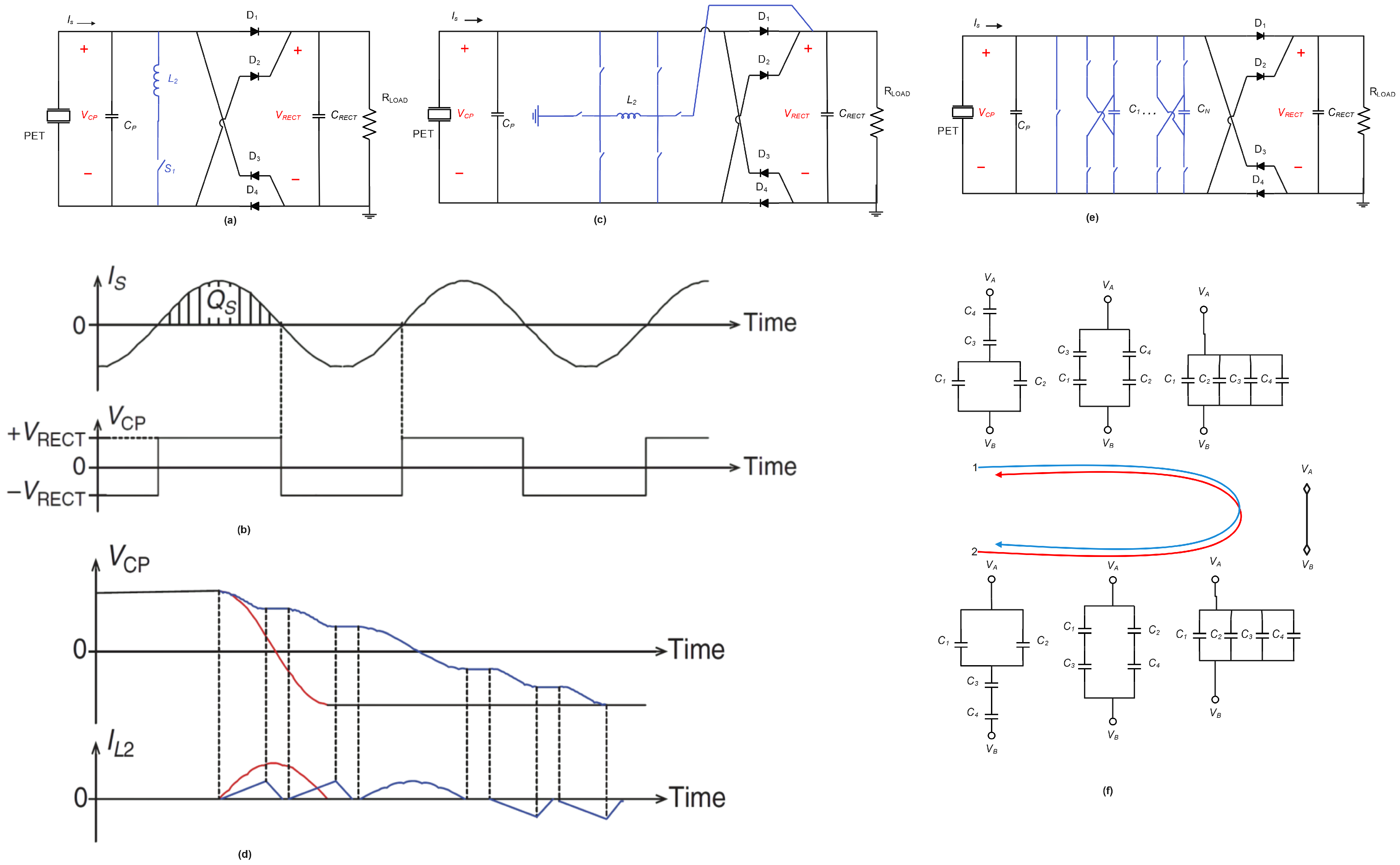
In the SSD-I
Figure 4b, an inductor (
) is introduced in series with the switch (
), converting electrical potential energy to magnetic energy. This generates a piezoelectric force that counteracts the original excitation force, resulting in more effective energy attenuation and vibration reduction compared to SSD-S in
Figure 4a.
Motivated by the SSD concept, SSH interfaces aim to harvest energy from mechanical vibrations while minimizing energy wastage during active switched damping. Various circuit topologies and control schemes have been proposed for SSH operations. However, precise switching and control circuits are required, and a common challenge lies in cold start-up situations when the system is deeply drained. To overcome this challenge, a parallel passive charging path is often incorporated alongside the primary power path.
SSH techniques can be categorized into two groups: open-circuit and short-circuit types. The open-circuit type, such as SECE and series SSHI, operates with the transducer under an open-circuit load most of the time. By optimizing the system to operate at the open-circuit voltage with Ω = when the series combination of inductor (), capacitor () and () reaches zero impedance, the current () can be maximized.
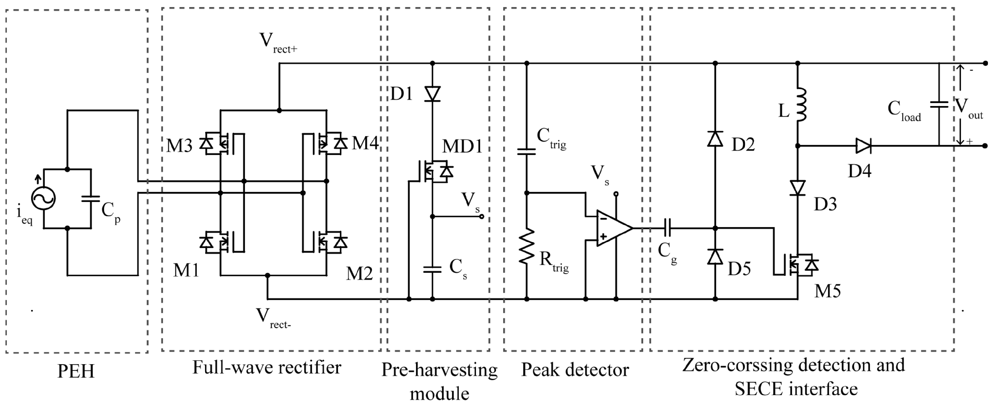
Conversely, the short-circuit type of SSH interfaces, including parallel SSHI and SSHC, regulate the voltage across by shorting the electrodes through the rectifier. By regulating the voltage in this manner, the transducer does not experience the effects of , and the extracted power reaches its peak at the resonant frequency when the inductor () resonates with the capacitor ().
These SSH techniques offer significant improvements in harvested power compared to traditional rectifiers. However, they require precise switching and control circuits and may face challenges during cold start-up. Incorporating a passive charging path provides a common solution to address this issue.
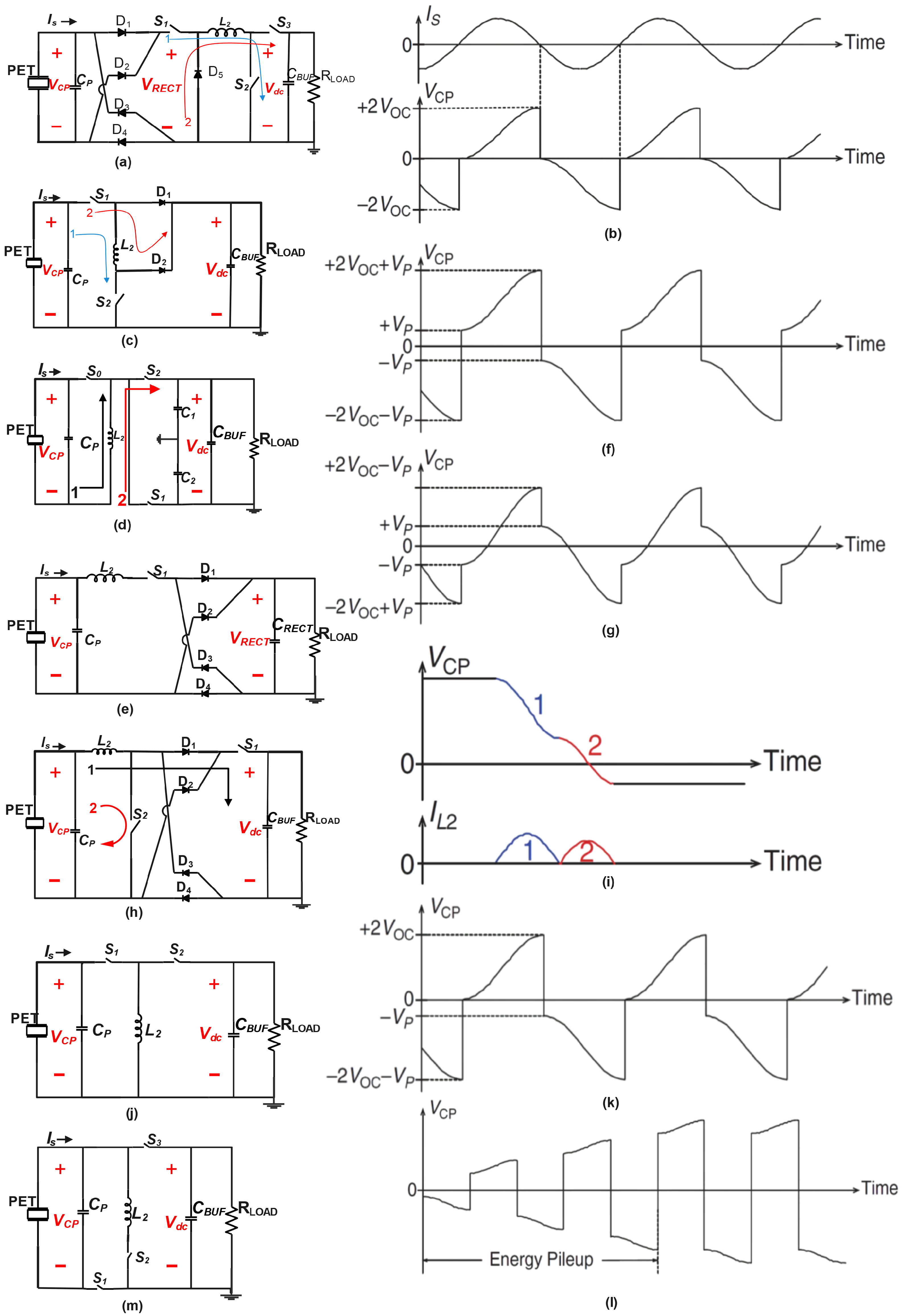
4.1. Open-Circuit Interface Circuits
4.1.1. Synchronous Electric Charge Extraction (SECE)
SECE, an open-circuit interface operation, was first introduced in [
4]. In the basic SECE architecture (
Figure 5a,b), the transducer is connected to a full-bridge rectifier (FBR), two switches (
and
), and an inductor (
) in series. Unlike the FBR architecture, SECE lacks a capacitor at the rectifier’s output. Instead, a buffer capacitor (
) is connected in parallel with the effective loading from the application circuits (
). It is linked to
using another switch (
) and a diode (
).
During operation, the switches remain mostly off while charges and discharges () in an open-circuit manner. Similar to SSD-S operation, SECE nullifies () the voltage across by activating and when the current through the transducer reaches zero crossings. However, instead of dissipating electrical energy as heat, SECE converts potential energy into magnetic energy in by turning on the switches for a controlled duration. After disconnecting from the transducer by deactivating and , another operation activates , converting the magnetic energy of the inductor into energy stored in .
Figure 5b illustrates the waveform, indicating that
is charged from 0 V to
during the positive current cycle. This implies that
potential energy can be harvested during each switching activity, resulting in four times higher extracted power (
) compared to an FBR or HBR. Despite the power consumed by active switching and the degradation of extracted power, the additional harvested power outweighs the power cost. In a specific implementation, a control circuit consumes 300 μW, while the extra harvested power is 3.85 mW [
22].
In another implementation illustrated in
Figure 5c, the rectifier is eliminated, resulting in a rectifierless SECE. During the switching activity, energy in
is transferred to
by activating
and
. In the subsequent operation, one of the switches is deactivated based on the signal polarity, and either
or
provides the current path to convert the inductor energy into energy stored in
. This implementation eliminates rectifier losses and achieves a mechanical-to-electrical conversion efficiency of 78% [
23]. However, it has the limitation of negative node voltages during operation, and D2 must remain off during positive current cycles, which requires the open-circuit voltage (
) to be lower than the DC voltage (
). This issue can be addressed by applying dynamic body biasing on S1.
Shareef et al. proposed a different rectifierless SECE implementation (
Figure 5d) using two capacitors (
and
) for positive and negative cycles, achieving a conversion efficiency of 73% [
24]. Nonetheless, this operation also results in negative voltages, requiring negative supplies.
To reduce conduction losses in switches, the current during energy transfer can be decreased by increasing the inductance of
. Gasnier et al. introduced multishot SECE operation, where potential energy in
is converted into
in multiple steps, reducing the peak inductor current and associated conduction losses. This design extracts 25% more power compared to traditional SECE [
25].
SECE offers the advantage of decoupling the interface operation from the load voltage
. This is possible because
is always completely discharged in SECE, resulting in an extracted power of
. However, SECE rarely harvests the full available power of the transducer due to specific conditions [
26].
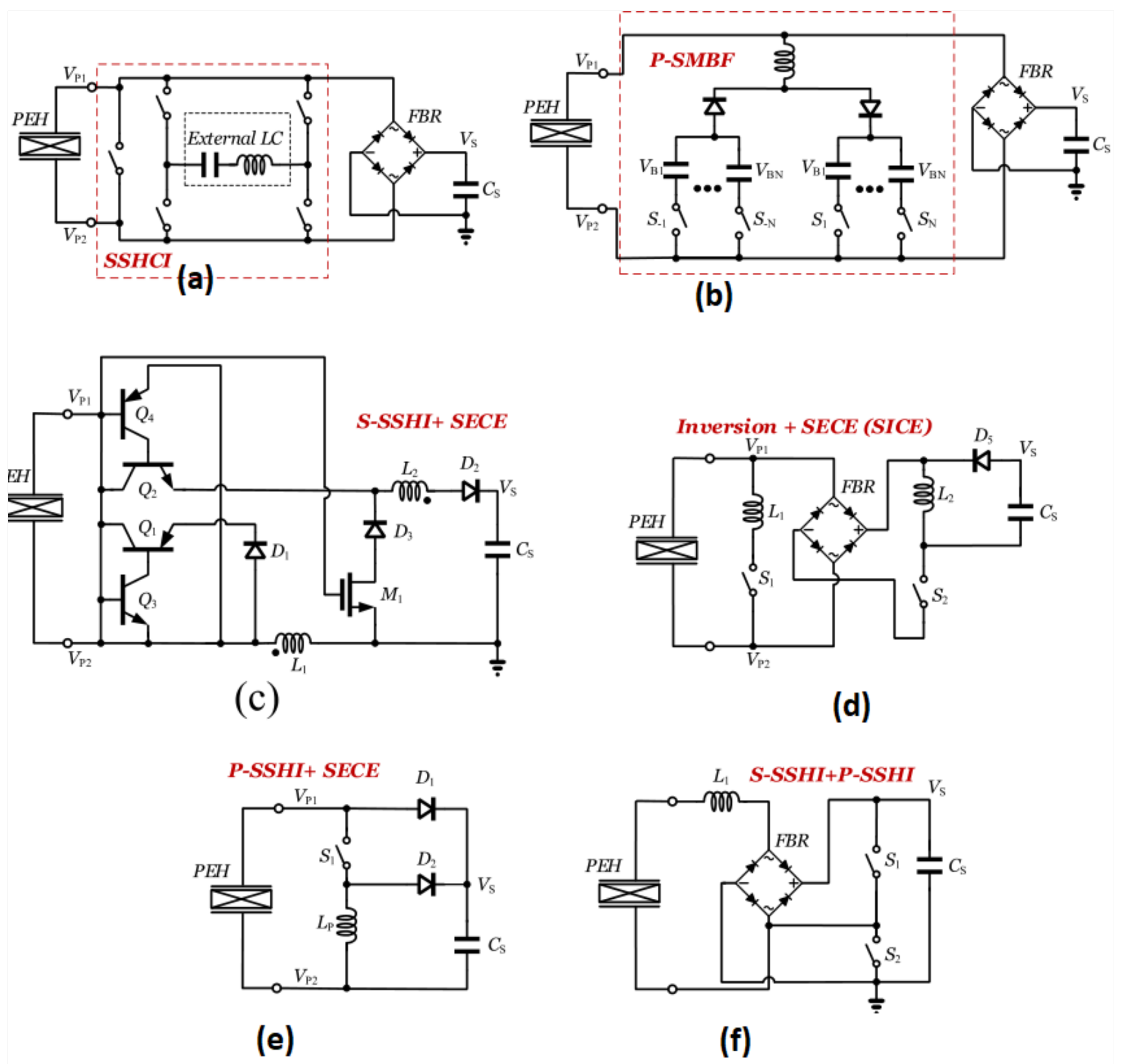
4.1.2. Predamping
The power extracted by the Synchronous Electric Charge Extraction (SECE) technique scales with the square of the open-circuit voltage (
) and maximizes at a power point (
) when
equals
. However, typical piezoelectric transducers exhibit a
significantly lower than
[
26]. While the full-bridge rectifier (FBR) charges the piezoelectric capacitor (
) from −
to +
, the SECE charges it from 0 V to 2
. Employing synchronous switching, it is feasible to precharge
to a voltage (
) exceeding 0 V immediately prior to the positive current cycle. This precharging method is termed “predamping” in the literature [
27].
An example of a predamping interface is the series synchronized switch harvesting on inductor (S-SSHI) circuit [
26], illustrated in
Figure 5e–g. This circuit resembles those in
Figure 6a,b, but with the FBR and switch+
positions interchanged. This maintains the same effective series combination and eliminates the need for two pads for the external inductor, while
remains dc in this particular configuration. During the positive peaks of
, switch
is activated, transferring energy from
to
via
. As
falls below
, the current through
diminishes, while
continues to discharge. Unlike the SECE, which deactivates
upon complete discharge of
, this method deactivates
when the inductor current reaches zero, thus negating the requirement for a de-energizing diode
.
When
exceeds 2
, this process can discharge
to a negative voltage (
), as depicted in the waveforms of
Figure 5f. This results in a positive predamped voltage (
) before the onset of the positive current cycle. The extracted power can be determined using equation
. Notably, when
= 0, the output power is equivalent to that of the SECE. However, if
is less than or equal to
, with
connected between the transducer and
,
remains above 0 V after the discharging switching event, preventing the intended “predamping” effect. In [
6,
28,
29], a two-step process is introduced, incorporating an additional voltage inversion after energy extraction.
Figure 5h,i depict a specific implementation [
6] utilizing a single inductor. The additional voltage inversion is facilitated by switch
, achieving the desired predamping. Furthermore, the energy extraction switch
is positioned after the rectifier, simplifying the implementation as
operates under a dc voltage.
Since S-SSHI shares the same circuit architecture as the SECE and differs only in the duration of
and
being turned on, predamping can be applied to various implementations of SECE by extending the ON time of
and
. Yang [
27] reported an output power that is 7.8 times higher than that of an FBR using the same architecture as shown in
Figure 5d.
It is worth noting that predamping by discharging
to a negative voltage (
) may not always improve performance. In some systems, predamping can lead to overdamping [
21], and in certain cases, ‘’less damping” is preferable with a
waveform as shown in
Figure 5g is desired [
6].
4.1.3. Energy Investing or Pileup
Building upon the earlier discourse regarding predamping, we now delve into a related concept put forth in [
3]. The proposed approach involves an energy-investing operation, which is visually represented in
Figure 5j,k. When
reaches its positive peaks,
is briefly connected across
before
is discharged. This initial connection sets an inductor current, effectively investing some energy. Then,
is connected to
, and the nonzero initial current helps drain
to a more negative voltage when the inductor current drops to zero. This boosts the damping and the extracted energy. It is important to note that the proposed operation is asymmetric, as energy is extracted only at negative
peaks, and it requires only two switches. However, the invested energy comes from the energy buffer, undergoing two additional transfers and associated losses compared to the harvested energy. Although the control circuit consumes only 630 nW, the reported conversion efficiency is 69%, and the maximum output power increasing rate is 247% [
3]. This segment delves into advanced techniques that enhance power extraction through dynamic switching strategies. The summary recaps how methods like Synchronous Electric Charge Extraction (SECE), various SSHI schemes, predamping, and energy investing effectively overcome the limitations of conventional rectifiers, despite introducing increased design complexity and demanding precise control.
In addition to the previously discussed techniques of predamping and energy investing, the authors of [
30,
31] introduce another innovative method known as energy pileup. This concept is illustrated in
Figure 5l. In the energy pileup mode, the design initially activates
when
reaches its peak. By carefully controlling the ON time, this operation achieves voltage inversion through
without extracting energy, allowing
to gradually accumulate. Once
reaches the desired value, typically constrained by the breakdown voltage of interface transistors, the operation transitions to the conventional S-SSHI energy transfer mode. Remarkably, the design presented in [
30] demonstrates a significant increase in the maximum output power rate, reaching up to 422% without the losses associated with energy investment.
Furthermore, Chamanian et al. [
32] propose a self-adapting Switched-Source Half-Bridge (SA-SSH) interface that utilizes only three switches, as depicted in
Figure 5m. This design performs energy pileup at positive peaks and energy extraction as well as investment at negative peaks. With this asymmetric operation, a more symmetric waveform can be maintained, reducing concerns about mechanical stability. An extracted power five times higher than that of an FBR is reported. In [
33], a thermoelectric generator (TEG) is combined with the piezoelectric transducer to accelerate the energy pileup process.
4.2. Short-Circuit Interface Circuits
In the previous section, we discussed the open-circuit type of SSH (Switched-Source Half-Bridge) interface, where energy extraction occurs only during short periods at zero crossings and voltage peaks. Now, we cover the second type of the SSH interface, known as the short-circuit type, which enables energy transfer for most of the cycle. By employing synchronized switching techniques, the energy transfer duration is maximized, leading to higher extracted power.
4.2.1. Utilizing Inductors
One well-known short-circuit interface operation is called P-SSHI or bias-flip interface. In this operation, the voltage inversion across the energy storage capacitor (
) is accelerated using a synchronized switched inductor, resulting in faster alternating path activation in the rectifier. This allows the transducer to primarily experience the effective loading through the rectifier, bypassing
. The extracted energy per cycle in this operation can be calculated as 2
, where
replaces the open-circuit voltage (
) in the SECE case, as shown in
Figure 6a,b. By tuning
to
/2, maximum power transfer (MPT) can be achieved. To improve the voltage inversion process, larger inductors are often used to reduce the inversion current and associated losses. A multistep P-SSHI design has also been proposed to enhance inversion efficiency;
Figure 6c,d.
In P-SSHI, proper setting of
is crucial for extracted power optimization. To achieve this, a switching dc–dc converter operating in discontinuous conduction mode (DCM) is commonly employed. This converter not only transfers the extracted energy to storage but also adjusts the effective loading by setting
, enabling MPT. A control scheme has been proposed to share the inductor for both interface bias flipping and the dc–dc converter, reducing the form factor [
1].
4.2.2. Inductorless Approaches
To reduce the size of the interface, an inductorless approach called P-SSHC has been proposed. This approach utilizes capacitors to achieve voltage flipping without the need for a large inductor [
34]. Multiple capacitors with the same capacitance as
are connected in parallel across the interface via switches. During the voltage-flipping process, the switches control the progressive sharing of charges between
and the capacitors, effectively reducing
. The capacitors are then connected back to
with the opposite polarity to increase
in the opposite direction as shown in
Figure 6e. This inductorless design achieves a flipping efficiency of 80%, but the required capacitors are currently too large for on-chip integration.
In a split-electrode piezoelectric transducer, implemented by Du and Seshia, on-chip capacitors are used in P-SSHC [
35]. The electrodes of the transducer are reconfigured to enable series or parallel connections, reducing the capacitance to be inverted during voltage flipping. Another switching scheme called flipping-capacitor rectifier (FCR) utilizes on-chip capacitors configured in series and parallel to achieve efficient voltage flipping [
36]. This scheme achieves a flipping efficiency of 85%. Further improvements have been made in capacitor switching algorithms to reduce intrinsic losses and enable the shared use of capacitors for interface bias flipping and the dc–dc converter.
Additionally, an experimental approach called ‘’SSH on an oscillator” has been proposed by Lallart et al. [
37], where
is connected to a second high-frequency piezoelectric oscillator during voltage flipping;
Figure 6f. This triggers a high-frequency mechanical vibration, enhancing the voltage inversion process. This design offers an inductorless and potentially more economically viable solution for SSH interfaces.
Focusing on short-circuit approaches such as P-SSHI and integrated MPPT strategies, this section illustrates how these circuits maximize energy transfer by extending the energy extraction window. The summary emphasizes the balance achieved between improved efficiency and the challenges of implementing synchronized switching under varying load and frequency conditions.
4.2.3. Maximum Power Point Tracking
Among the discussed interface circuits, the SECE circuit stands out as the only one where output power depends solely on (open-circuit voltage). In SECE, the energy in is harvested completely whenever its voltage peaks. This decouples energy harvesting from the load condition, and the output power is determined by , which is influenced by vibration, mechanical parameters, and .
On the contrary, in all other interface circuits, the extracted power relies on specific voltages such as . These voltages, like the amplitude set by in FBR/HBR and short-circuit interfaces or the predamping voltage VP in open-circuit cases, depend on the effective load . A switching dc–dc converter in the discontinuous conduction mode (DCM) is often used to emulate a resistive load. The effective and resulting can be adjusted by altering the switching timing. For instance, the output power of FBR is given by the expression 4, which reaches its peak when is set such that = . Due to this dependency, an MPPT (Maximum Power Point Tracking) circuit is required for all interface circuits except SECE.
MPPT circuits can be broadly categorized into two types: (1) open-loop “fractional
” methods and (2) closed-loop approaches like “P&O”. In fractional
techniques,
is periodically measured by disconnecting the interface circuit from the transducer, as shown in
Figure 7a. A passive or active peak detector is used to sense
, and techniques like voltage division or charge sharing generate the desired fractional voltage for reference. The switching timing of a subsequent buck–boost dc–dc converter is then adjusted to achieve MPPT. On the other hand, closed-loop methods continuously measure the output power while the harvester is connected to the transducer. Algorithms such as hill climbing are used to adjust operating parameters for maximizing the output power within the measurement tolerance. MPPT circuits perform two tasks: sensing and tuning.
In the fractional
method,
is sensed periodically with a low duty cycle by disconnecting the harvester from the transducer [
12,
38]. Passive or active peak detectors are used, and techniques like resistive ladder voltage division or charge sharing are employed to generate the desired fractional voltage. The switching timing of a subsequent buck–boost dc–dc converter is adjusted accordingly to set
to the desired fractional voltage, achieving MPPT [
38]. Various examples of this method have been proposed, demonstrating high power-harvesting efficiency and fast tracking times.
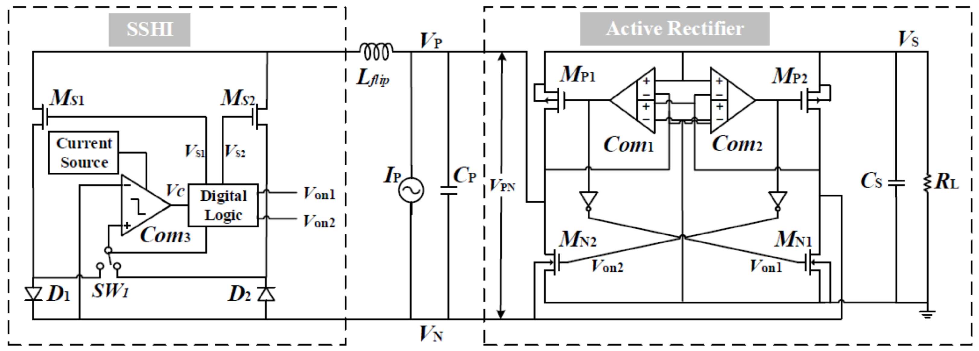
Another approach, the ‘’sense-and-set” method [
12], oversamples the current (
) and calculates the instant
using a mixed-signal circuit. IS is measured by charging
for a short period, and the resulting small voltage is amplified and transferred to a capacitor to indicate IS. Combined with high-frequency open-circuit interface operation, this method maintains
dynamically across
, resulting in improved power extraction compared to an FBR. This approach showcases the potential of advanced IC technology in implementing complex control schemes to enhance power extraction for vibrational energy harvesting.
4.2.4. Perturb and Observe (P&O)
The Perturb and Observe (P&O) method is a closed-loop MPPT technique that aims to maximize the output power by directly measuring a physical quantity that indicates the extracted power. One implementation of P&O involves using a flyback converter with constant ON time modulation, where the peak inductor current is measured through a small sensing resistor to determine the extracted power. The sensing voltage is digitized using an analog-to-digital converter, and a digital circuit in a low-power microcontroller unit (MCU) implements the P&O algorithm. This approach has shown an MPPT efficiency above 94% [
13].
Another fully mixed-signal implementation evaluates the extracted power by multiplying the converter’s input voltage and current [
40]. By biasing the MOSFET in the subthreshold region to exploit logarithmic current–voltage characteristics, the power level indication is obtained through current summation. This design achieved an end-to-end efficiency peak of 88% and an MPPT peak efficiency of 99.8%. While the mentioned implementations are suitable for electrostatic energy harvesting, they can be applied to piezoelectric energy harvesting as well.
4.2.5. Nonresonant Operation
The discussed interface circuits primarily focus on achieving resistive loading, assuming that the impedance of a piezoelectric cantilever vibrating near its resonant frequency is mostly resistive [
7,
13]. However, in real-world applications like infrastructure or factory monitoring, the operating frequency may deviate from the piezo structure’s resonant frequency. This frequency offset leads to a reactive impedance that cannot be effectively matched with a purely resistive load, resulting in a significant degradation of the extracted power. To address this issue, Hsieh et al. proposed a method to achieve complex impedance matching by introducing a delay in the conventional switching methods [
7]. By creating a phase offset between the interface voltage and current, the interface circuit presents a complex loading. The resistive part extracts power from the source, while the reactive part cancels the residual reactance of the piezoelectric structure. Adjusting the equivalent loading through variations in
and switching timing optimizes the extracted power. This intentional delay can be incorporated into both open-circuit and short-circuit interface types, improving harvesting performance when operating off-resonance. Experimental results have shown significant bandwidth extensions and improved power extraction efficiency [
8,
41,
42,
43].
4.2.6. Charging Efficiency Analysis
The charging efficiency of piezoelectric energy harvesting varies significantly among different interface circuits, ranging from basic to advanced topologies. Standard full-bridge rectifiers offer simplicity but limited efficiency (20–30%), while voltage doublers achieve slightly higher efficiency (30–40%) with increased output voltage. Advanced techniques such as Synchronized Switch Harvesting on Inductor (SSHI) demonstrate marked improvements, with parallel SSHI reaching 40–60% efficiency and series SSHI achieving 50–70%. The Synchronized Electrical Charge Extraction (SECE) technique shows the highest efficiency (60–80%) and offers load-independent operation, though with increased implementation complexity. Charging efficiency is influenced by multiple factors, including circuit parameters, operating conditions, and system integration aspects. Optimization strategies focus on component selection, control methods, and system design considerations such as impedance matching and parasitic minimization. The selection of interface circuits should balance efficiency requirements against implementation complexity and cost constraints, considering specific application needs in self-powered systems.
6. Discussion of Performance Enhancement
Table 1 and
Table 2 quantitatively assess the performance enhancements achieved by the interface circuits under review, utilizing the Maximum Output Power Improvement Rate (MOPIR) and conversion efficiency (
) as key performance indicators. These technologies are summarized and visually represented in
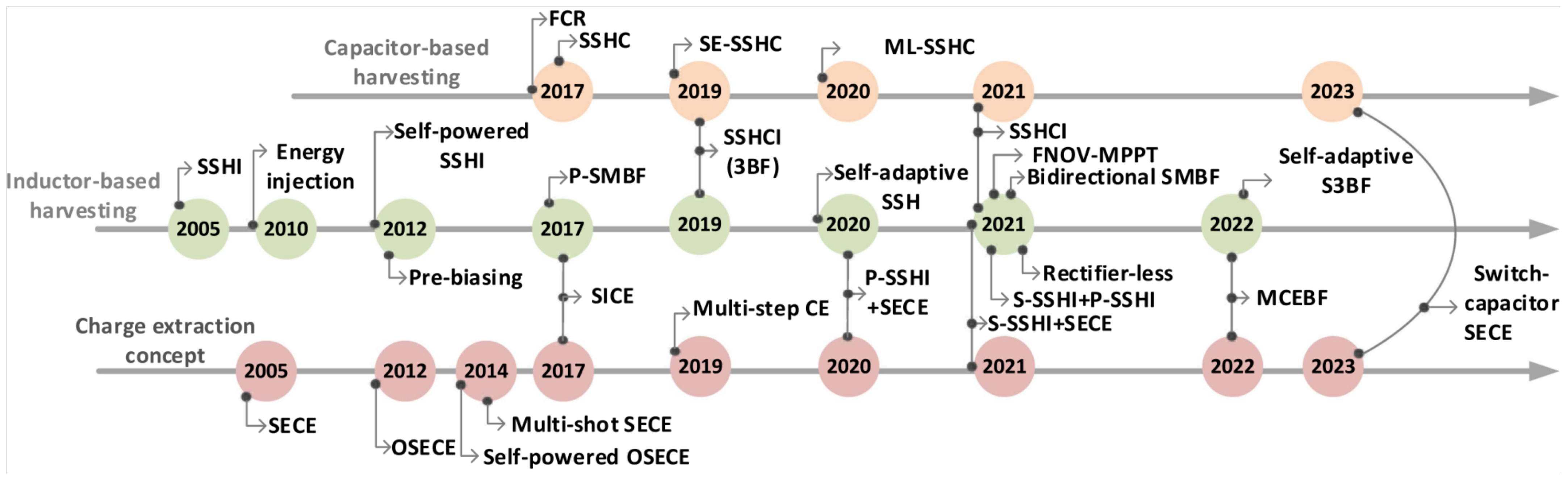
Figure 18, which illustrates the progress made over the years 2005–2023.
These metrics, rigorously defined and widely adopted within the power electronics and energy harvesting research communities, as evidenced by publications in prestigious journals such as
IEEE Transactions on Power Electronics,
IEEE Journal of Solid-State Circuits,
IEEE Transactions on Industrial Electronics, and
IEEE Transactions on Circuits and Systems I and II, provide a standardized framework for objective comparison. Specifically, MOPIR, formulated as in Equation (
5) and defined by Xie et al. [
63], normalizes the power improvement relative to the conventional full-bridge rectifier (FBR), while the conversion efficiency
, detailed in Equation (
6) and defined by Badr et al. [
64], quantifies the effectiveness of power conversion by considering power losses.
Figure 18.
Progress on the synchronous switch harvesting energy over the years of 2005–2023 [
65].
Figure 18.
Progress on the synchronous switch harvesting energy over the years of 2005–2023 [
65].
Table 1.
Comparison of Interface Circuits for Piezoelectric Energy Harvesting.
Table 1.
Comparison of Interface Circuits for Piezoelectric Energy Harvesting.
| Interface | Technology | Voc (V) | Power (µW) and Efficiency | Frequency (Hz) | Key Features/PZT | Load Depend./SP |
|---|
| FTSCR [63] | 0.18 µm CMOS | 3 | 4.84 µW, 8.14x | 57 | C = 800 pF, On-Chip, PZT5A | No, No |
| SICE [53] | Discrete | 5.2 | 380 µW, 5x | N/A | L1 = L2 = 1 H, Custom PZT | No, No |
| FCR [66] | 0.18 µm CMOS | 2–8.5 | 50.2 µW, 4.83x | 110 k | C = 1.44 nF On-Chip, MIDE V21B, V22B | Yes, No |
| SE-SSHC [2] | 0.18 µm CMOS | 2.5 | 186 µW, 8.2x | 219 | Ctotal = 4 nF, On-Chip, Custom MEMS | Yes, No |
| MSBF [67] | 0.13 µm CMOS | 1.5 | 63 µW, 4.48x | 441 | L = 47 µH, Cb = 14 nF, Cross-coupled FBR, Off-Chip, MIDE PPA-1022 | Yes, No |
| S-SSHI-phi [6] | 0.25 µm HV CMOS | 2.5 | 228.8 µW, 8.27x | 126.7 | C = 15.9 nF, Cross-coupled FBR, Mide V22B | Yes, No |
| FCR Split-Phase [5] | 0.18 µm CMOS | 3 | 33.1 µW, 9.2x | 200 | C = 22 nF, Cross-coupled P/NMOS/Frac Voc, Mide PPA-1021 | Yes, No |
| Sense/set MPPT [39] | 0.18 µm CMOS | 1.5 | 2.76 µW, 5.41x | 85 | C = 10 nF, MOS switches/Frac Voc, Mide PA-1022 | Yes, No |
| SECE tuning/sensing [8] | 0.6 µm CMOS | 3 | 275 µW, 3.31x | 56 | C = 24 nF, Cross-coupled FBR P&O, Frac Voc | Yes, No |
| VM-SECE [10] | 0.35 µm CMOS | 4 | 13.5 µW, 2.43 | 90–160 | C = 17–49 nF, Active FBR | Yes, No |
Table 2.
Comparison of Interface Circuits for Self-Powered Systems.
Table 2.
Comparison of Interface Circuits for Self-Powered Systems.
| Interface | Technology | Voc (V) | Power and Efficiency | Frequency (Hz) | Key Features/PZT | Load Depend./Year |
|---|
| P-S3BF [51] | Discrete | 15 | 470 µW, 2.87x | 24.9 | L = 47 µH, Cb = 4.7 µF, Off-Chip, PZT-5A | Yes, 2018 |
| SSHCI [48] | 0.18 µm CMOS | 3.2 | 13 µW, 5.44x | 415 | L = 100 µH, C = 2 nF, Off-Chip, Custom MEMS | Yes, 2021 |
| ML-SSHC [68] | 0.18 µm CMOS | 1.27–2.34 | 1.51–4.85 µW, 8.7x | 22 | Ctotal = 600 pF, On-Chip, VH1504C-2 | Yes, 2020 |
| SSHC [34] | 0.35 µm CMOS | 2.5 | 161.8 µW, 9.7x | 92 | C = 45 nF, Off-Chip, MIDE V21BL | Yes, 2017 |
| S-SSHI+SECE [52] | Discrete | 6 | 280 µW, 7.28x | 18 | L1 = L2 = 2.21 mH, MIDE PPA-2011 | Medium, 2020 |
| P-SSHI+SECE [52] | Discrete | 3 | 85.7 µW, 2x | 23 | L = 1.5 mH, PZT-5H | Medium, 2020 |
| S/P-SSHI [54] | Discrete | 5 | 112 µW, 3.2x | 70 | L = 1.5 mH, Custom PZT | Medium, 2021 |
| NYC-PSSHI [69] | Discrete | 3–7 | Up to 300 µW, 8.21x | 100–500 | L = 100 µH, MIDE PPA-1001 | Yes, 2018 |
| P-SSHI [20] | - | 1.8 | 11.15 µW, - | 5 | optimal load: Ropt = 400 kΩ | Yes, 2017 |
| Adapt. SSHI [45] | 0.18 µm CMOS | - | 11.15 µW, 4.6x | 5 | optimal load: Ropt = 400 kΩ | Yes, 2020 |
| ReL-SSHI [46] | 0.18 µm CMOS | 1.6–1.8 | -, 4.6x | 18.6 | - | -, 2021 |
| ZSECE [18] | Discrete | - | -, 7.93x | 18.6 | - | No, 2022 |
| BL-S-SSHI [19] | Discrete | - | -, 3x | 18.6 | voltage doubler | -, 2021 |
| MI-P-SSHI [17] | - | - | -, - | - | phase mismatch of multiple sources | -, 2022 |
| SPEDS-SSHI [16] | - | 5.2–5.8 | -, 4.6x | - | RC differential circuit, extensible | Yes, 2022 |
| CHP-AM [70] | Discrete | 16.5 | 170 µW, 1.89x | 24 | circular hole-based | Yes, 2024 |
| SP-MIHR [71] | - | 4.5–6.5 | -, 4.7x | - | multiple PZTs, arbitrary phase difference, low start-up voltage, | Yes, 2024 |
| MSP-SICE [72] | Discrete | 1.88–6.5 | 215 µW, x | 8–8.4 | mH, PZT-4 | Yes kΩ, 2024 |
| SS-TEPG [73] | - | 30.5–151 | 1.9–8.2 mW, x | 8.3–31.2 | LTC 3588-based hybridized power management (L-HPM) | Yes, 2024 |
| AR-SBC [74] | 0.18 µm HV | 3.9 | 14.1 mW @ 1 kΩ, x | 20 | self-biased comparator | Yes kΩ, 2024 |
| EP–SSHI–TEA [75] | Discrete | 6–8 | 400 µW, 3.63x | 34 | multiple PZTs | Yes, 2023 |
| SP-P-PV [76] | 180 nm CMOS | 3.3/0.6 | 189 µW, - | 43 | L1 = L2 = 2.21 mH, C1 = C2 = 220 µF, Vsto = 22 µF, PZT-5H | Yes, 2024 |
| A-pre-bias-MPPT [77] | 0.18 µm HV | 0.3–1 | 32.44 nW, 12.68x | 146 | L = 47 µH,SADPM | Yes, 2024 |
| GI-DR [78] | - | 15 | 3.17 µW, 7.63x | 20 | mF, mH, Ω, gyrator-induced, | Yes, 2024 |
| HTG [79] | - | 4.5–6.5 | 14.58 mW, 4.7x | 8 | MΩ | Yes, 2024 |
Our comparative analysis definitively demonstrates that while traditional rectifier-based circuits, such as the FBR and half-bridge rectifier, offer design simplicity, their achievable performance is fundamentally constrained by inherent limitations. These limitations primarily stem from voltage drops across rectifying diodes and suboptimal impedance matching to the piezoelectric transducer, thereby restricting the overall power extraction efficiency. Conversely, a significant paradigm shift in performance is observed with advanced interface circuits employing synchronous switching techniques. Methodologies like Synchronous Electric Charge Extraction (SECE) [
2] and Synchronous Switch Harvesting on Inductor (SSHI) schemes [
34] effectively overcome these limitations, enabling substantially higher power extraction by actively managing the charge transfer and optimizing impedance conditions. Inductor-based hybrid interface circuits, as explored in studies by Xia et al. [
52,
54,
80], further exemplify this trend. Their ease of implementation with minimal discrete components belies their capacity to achieve high MOPIR, particularly under conditions of higher input excitation, showcasing the benefits of inductive elements in resonant energy harvesting scenarios. Furthermore, leveraging CMOS technology for techniques like multiple bias flipping, as investigated by Javvaji et al. [
67], has been shown to yield MOPIR enhancements exceeding fourfold, demonstrating the effectiveness of integrated circuit implementations for advanced control. As highlighted by Badr et al. [
64], achieving high output power levels enables the implementation of self-powered, precise switching control mechanisms, such as in P-SSHI, which in turn minimizes power dissipation associated with control overhead.
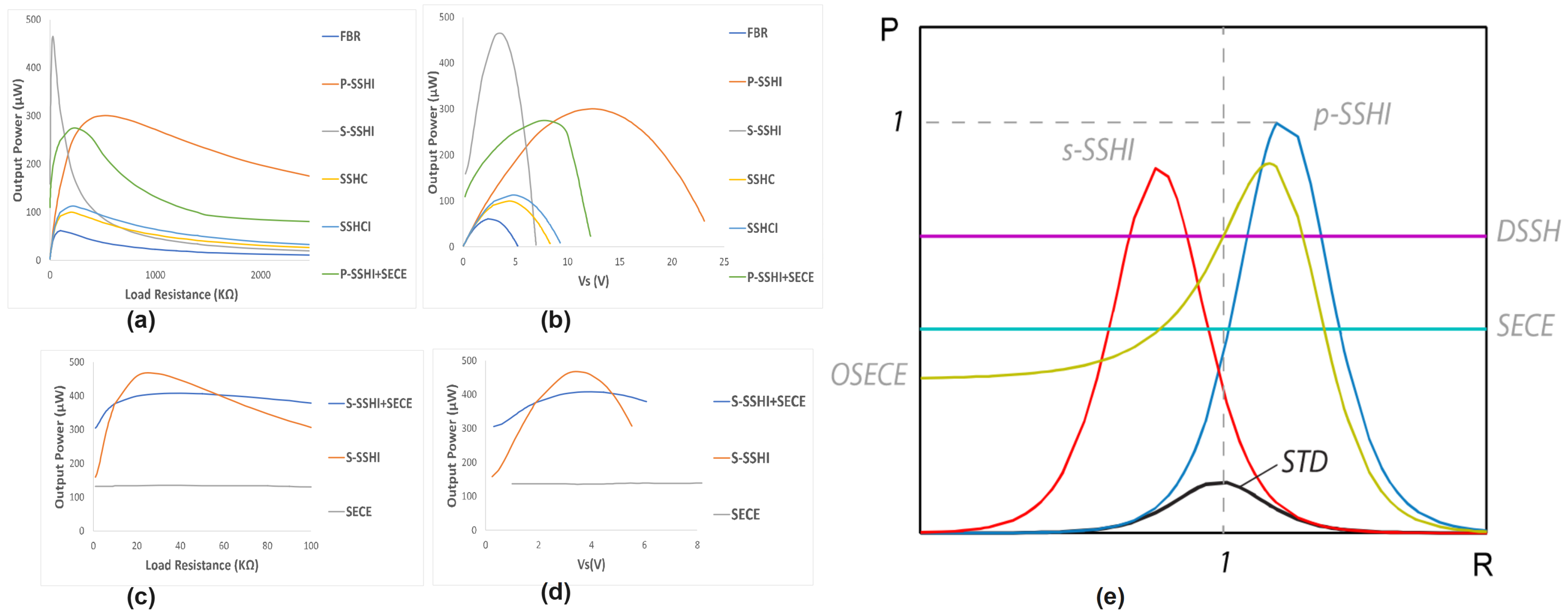
To further clarify these performance characteristics, LTspice simulations were performed using a representative piezoelectric energy harvester (PEH) model. The simulations evaluated the various interface circuits listed in
Table 1, and the top-performing configurations are summarized in
Table 3. As illustrated in
Figure 19a, these simulations underscore the critical role of Maximum Power Point Tracking (MPPT) modules, especially for SSHI-based techniques. The inherent load dependency of SSHI circuits necessitates MPPT for optimal impedance matching and maximized power extraction. The reduced power observed in SSHCI [
48] simulations, as seen in
Figure 19a, can be attributed to the increased complexity of its digital control unit required for managing more intricate switching phases, highlighting a trade-off between control sophistication and overall power efficiency. While SSHC configurations which eliminate the bulky inductor achieve inductor size reduction, this comes at the cost of lower output power due to capacitor-based configuration limitations and more complex switching requirements.
Figure 19b further clarifies that the optimal rectified voltage (
) in S-SSHI is inherently lower than that in P-SSHI configurations, a key design consideration for system integration. As anticipated from theoretical analysis, SECE demonstrates a near-linear output power response across load variations, indicating its inherent load independence, whereas hybrid techniques combining S-SSHI and SECE, as shown by Xia et al. [
52] [
Figure 19c], effectively smooth out the power output profile of S-SSHI, enhancing its robustness under varying load conditions. Furthermore, as depicted in
Figure 19d, varying the rectified voltage reveals the output power of SECE to be largely insensitive to voltage changes, contrasting with S-SSHI whose output power is significantly affected with the hybrid technique exhibiting a reduced sensitivity compared to standalone S-SSHI.
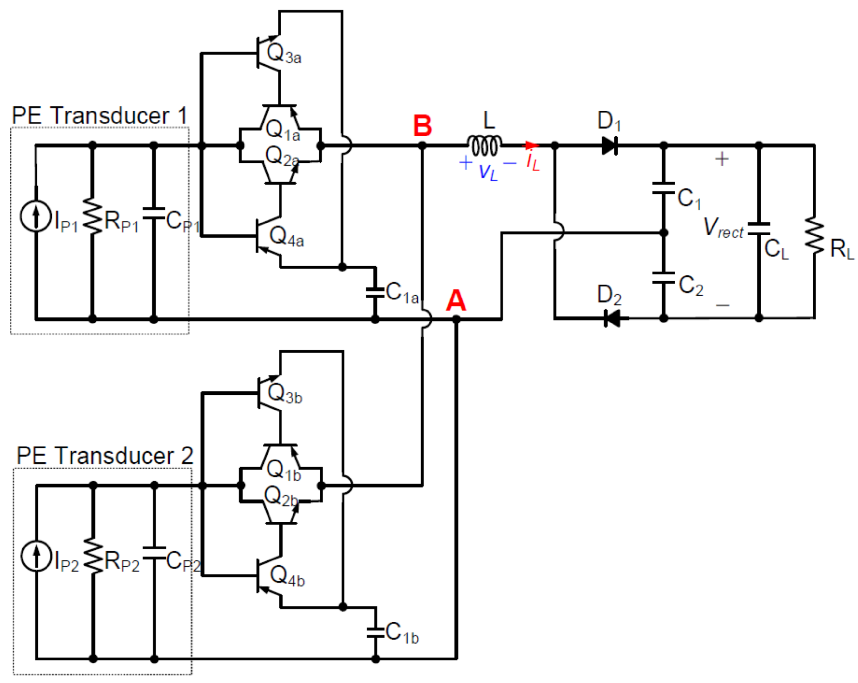
The Self-Powered Multi-Input Hybrid Rectifier (SP-MIHR) [
71] stands out as a particularly advanced solution, showcasing a superior end-to-end conversion efficiency of 67.3% and a maximum output power 1.47 times greater than classical S-SSHI circuits. Notably, the SP-MIHR also achieves a 0.5 V reduction in start-up voltage and exhibits a 4.12-fold power improvement and 1.3-fold voltage enhancement over standard multi-input energy harvesting circuits, all while maintaining a structurally simple and scalable architecture [
4]. While SSHC [
34] offers a compromise between complexity and implementation ease by using off-chip components and SSHCI [
48] reduces inductor size using a capacitor-inductor hybrid approach (albeit still with off-chip components), SE-SSHC [
2] and FTSCR [
63] represent alternative topologies prioritizing ease of implementation by eliminating the need for off-chip components altogether.
In addition to interface circuit innovations, advancements in transducer designs also play a critical synergistic role in enhancing overall energy harvesting system performance. For example, the circular hole-based piezoelectric energy harvester demonstrates a substantial 13.8% increase in open-circuit voltage, resulting in an approximate 89% improvement in harvested energy. The practical efficacy of these combined advancements is further underscored by the successful integration of such harvesters with low-power voltage regulators [
2], highlighting their suitability for real-world self-powered system implementations.
However, despite the significant performance gains achieved in laboratory settings, the scalability of these advanced interface circuits for industrial-scale piezoelectric energy harvesting remains a crucial consideration for widespread practical deployment. Maintaining the demonstrated high efficiency and performance metrics as production scales presents substantial challenges. These include mitigating the impact of component variations inherent in mass manufacturing, managing increased parasitic effects in larger circuit layouts, and ensuring the robust and consistent operation of complex control strategies in mass-produced circuits. Furthermore, the economic viability of implementing sophisticated control circuitry, particularly for techniques like SECE and SSH, needs careful evaluation against the cost-effectiveness and robustness of simpler circuit designs for different application contexts. Addressing these scalability challenges requires focused future research and development efforts aimed at optimizing designs for manufacturability, developing robust and easily implementable control strategies, and carefully selecting cost-effective components without compromising performance. Such efforts are essential to bridge the gap between laboratory-proven performance and the practical feasibility of deploying high-performance interface circuits in large-scale piezoelectric energy harvesting systems.
In conclusion, realizing truly optimal piezoelectric energy harvesting necessitates a careful balancing of inherent trade-offs [
1]. Key design considerations include circuit complexity, the precision and adaptability of calibration methodologies [
9], and the effectiveness of impedance matching strategies, including those achieved through intentional delays in switching timing as discussed in state-of-the-art reviews [
81]. These factors become particularly critical in complex systems integrating multiple piezoelectric transducers, especially those operating under diverse and asynchronous vibrational excitations. A judicious balance across these design parameters is paramount to fully unlock the potential of advanced energy harvesting interface circuits and facilitate their widespread adoption in practical self-powered applications.
7. Conclusions
The evolution of interface circuits for piezoelectric energy harvesting in self-powered systems is propelled by a continuous drive for enhanced efficiency, miniaturization, and intelligent control. This relentless pursuit is reflected in current trends focusing on advanced rectification techniques, adaptive impedance matching algorithms like Maximum Power Point Tracking (MPPT), and sophisticated energy management systems—all aimed at maximizing power extraction and storage. As highlighted in this comprehensive review of power conditioning techniques, these advancements mark a significant stride from traditional rectification towards cutting-edge strategies. Our investigation reveals that innovative circuit topologies like the SP-MIHR, SPEDS-SSHI, ZSECE, MI-P-SSHI, BL-S-SSHI and P-SSHI alongside transducer advancements such as the circular hole-based harvester are key enablers for enhanced efficiency, increased power output, and improved robustness in self-powered piezoelectric energy harvesting systems. Key findings underscore the superior performance of advanced topologies utilizing synchronous switching and dynamic impedance matching and further emphasize the multifaceted benefits of the mentioned topologies, while innovative transducer designs demonstrably amplify system performance. Further progression in this field includes System-on-Chip (SoC) integration for footprint reduction, low-power design for minimized losses, and application-specific optimizations tailored for diverse applications ranging from wearables and IoT devices to structural health monitoring. While both piezoelectric and magnetoelectric (ME) devices are employed for energy harvesting in self-powered systems, their differing transduction mechanisms necessitate distinct interface circuit designs. Piezoelectric harvesters, converting mechanical strain to electrical energy, typically generate high-voltage, low-current AC signals, optimally paired with high-impedance circuits. In contrast, magnetoelectric harvesters, which harness magnetic field variations, often produce lower voltage and current levels with lower impedance, sometimes even DC output. Consequently, directly applying a piezoelectric-specific interface circuit to an ME harvester would likely result in significant power loss and inefficient operation due to impedance mismatch and incompatible voltage/current handling. Adapting interface circuits to match the specific output characteristics, frequency response, and potential biasing needs of ME devices is therefore crucial for achieving optimal energy harvesting efficiency in self-powered systems utilizing magnetoelectric conversion. These collective advancements, including circuits tailored for specific transducer types, pave the way for viable self-powered systems. However, realizing widespread adoption requires strategically tackling persistent challenges, notably in control circuit power consumption, scalability, long-term reliability, and environmental impact. This review provides a comprehensive overview of recent advancements in interface circuits for piezoelectric energy harvesting systems, highlighting innovative designs, improved control methodologies, and enhanced power extraction techniques. Notably, the continuous development of advanced methods such as SECE, SSH, and active MPPT algorithms are addressing long-standing challenges in efficiency and reliability. However, as we discuss, scalability remains a significant hurdle for industrial-scale implementation. In addition, the integration of intelligent control strategies and the exploration of eco-friendly materials are promising directions for future research. Addressing these areas is critical to advancing the practical deployment of self-powered systems across applications ranging from wearable electronics to structural health monitoring. Future research must therefore prioritize broadening comparative analyses, optimizing low-power control, rigorous real-world validation, and addressing sustainability through life cycle assessments and eco-friendly materials. Ultimately, by overcoming these hurdles and continuing on the current trajectory of development, the field of piezoelectric energy harvesting, alongside adapted approaches for magnetoelectric systems, is poised to deliver highly efficient, robust, and adaptable interface circuits. These circuits will be crucial enablers for the widespread deployment of truly self-powered systems across diverse fields, fostering a more energy-independent and environmentally conscious future.


