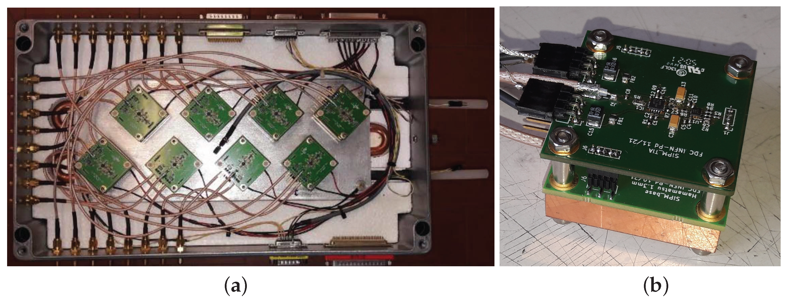
Figure 1.
(a) the dark box with 8 SiPM modules mounted over a cooling plate. (b) the SiPM module.
Figure 1.
(a) the dark box with 8 SiPM modules mounted over a cooling plate. (b) the SiPM module.
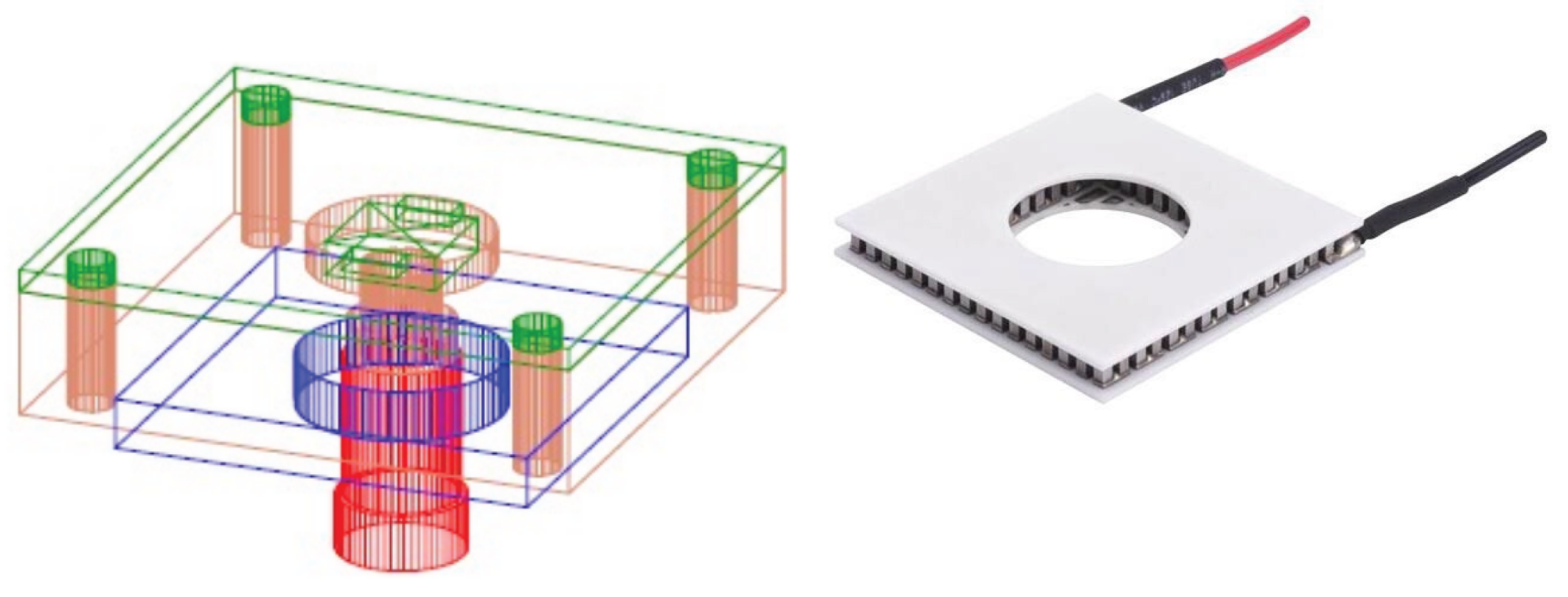
Figure 2.
On the left the scheme illustrating the positioning of the Peltier cell with respect to the copper block; the red cone in the center is the quartz fiber head illuminating the SiPM. On the right the Peltier cell with a central hole to allow the laser illumination.
Figure 2.
On the left the scheme illustrating the positioning of the Peltier cell with respect to the copper block; the red cone in the center is the quartz fiber head illuminating the SiPM. On the right the Peltier cell with a central hole to allow the laser illumination.
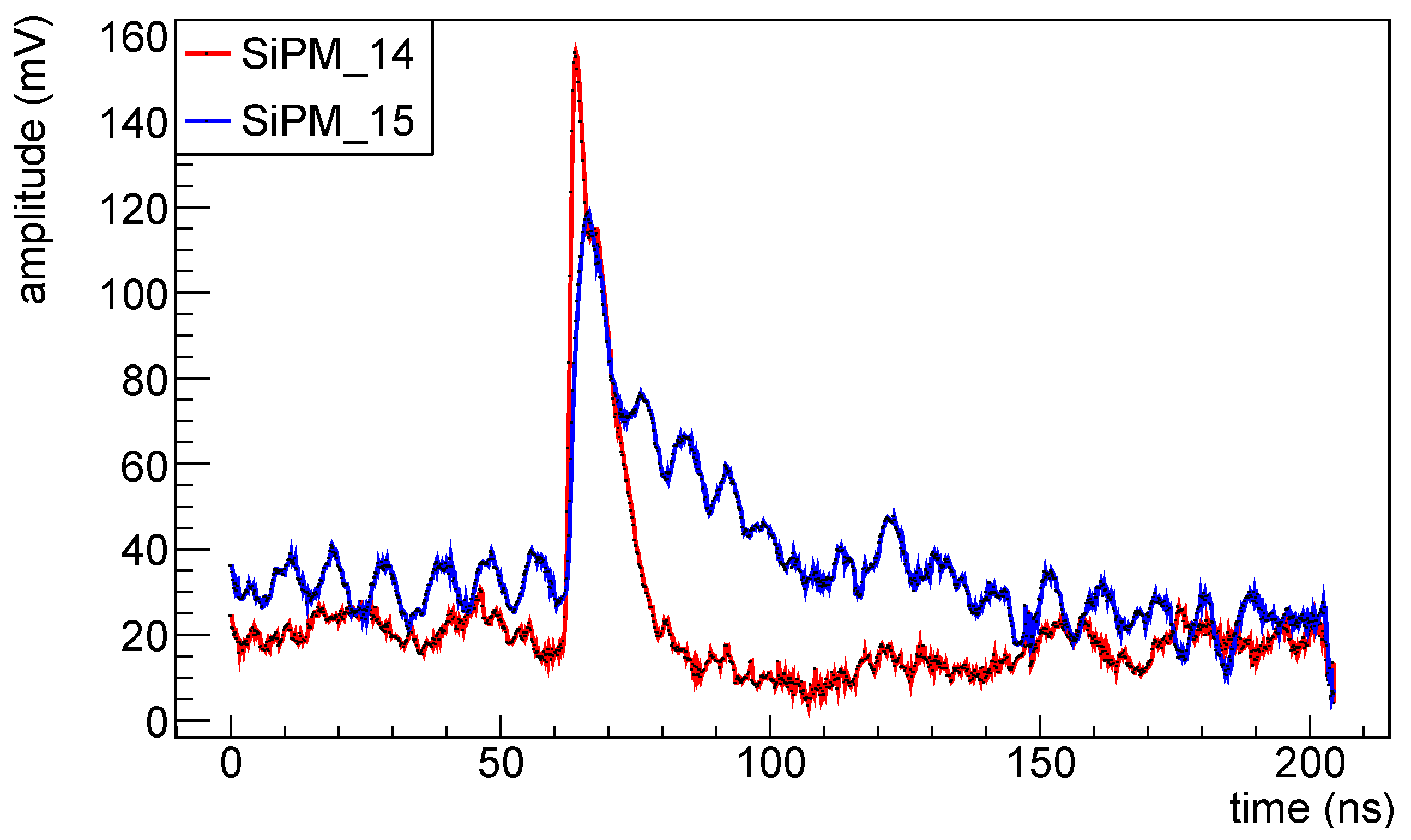
Figure 3.
Waveforms for two different SiPMs before irradiation: in red SiPM (FBK ) and in blue (Hamamatsu ).
Figure 3.
Waveforms for two different SiPMs before irradiation: in red SiPM (FBK ) and in blue (Hamamatsu ).
Figure 4.
SiPMS board irradiated inside the CN beam line.
Figure 4.
SiPMS board irradiated inside the CN beam line.
Figure 5.
Microscope picture of SiPM .
Figure 5.
Microscope picture of SiPM .
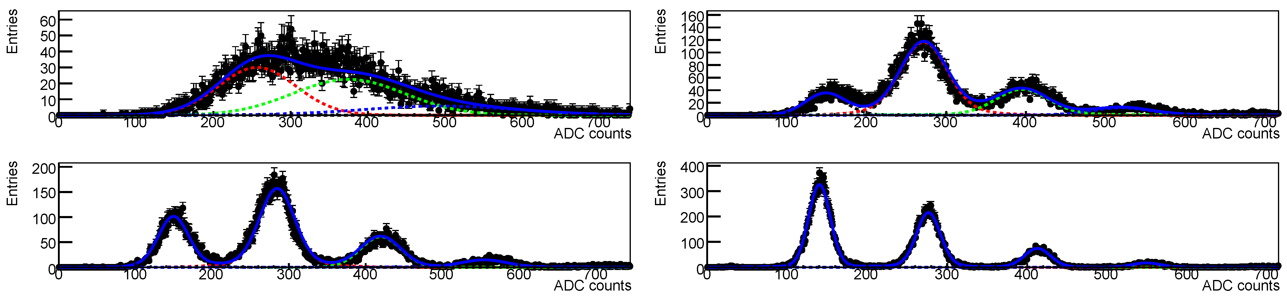
Figure 6.
Photon spectra for SiPM , after first irradiation at neq/cm2, at different temperatures. From top to bottom spectra taken at temperatures of 10 °C, −10 °C, −20 °C and −35 °C. The spectra are taken at the same overvoltage (2 V). The colored curves correspond to the different photon peak contributions to the poissonian.
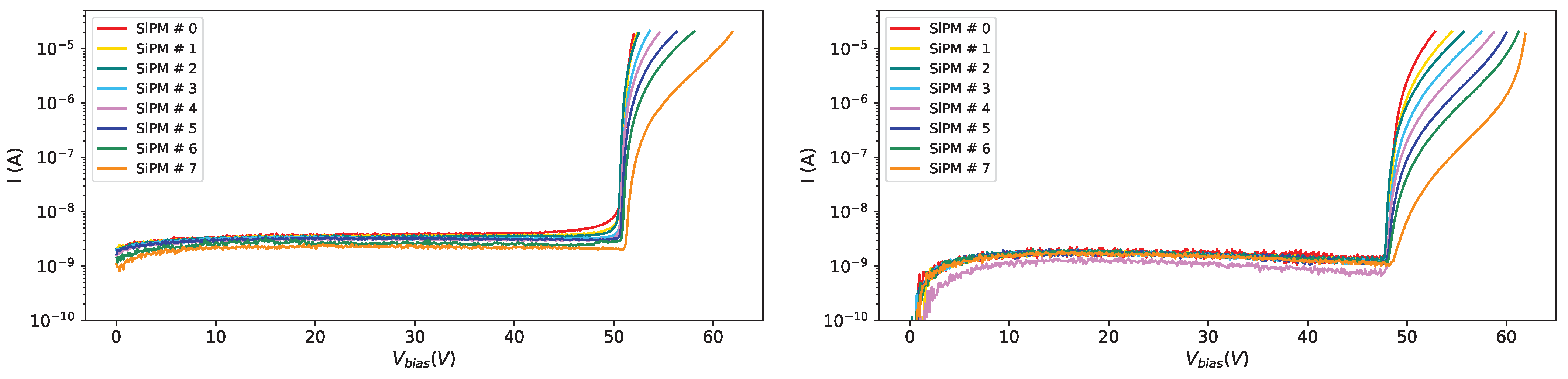
Figure 7.
IV-curves for SiPMs of set H1 after first irradiation campaign. Curves for all SiPMs, at 10 °C on the (left) and at −40 °C on the (right).
Figure 7.
IV-curves for SiPMs of set H1 after first irradiation campaign. Curves for all SiPMs, at 10 °C on the (left) and at −40 °C on the (right).
Figure 8.
IV-curves for SiPMs of set H1 after first irradiation campaign. Curves for all temperatures, for SiPM on the (left) and for SiPM on the (right).
Figure 8.
IV-curves for SiPMs of set H1 after first irradiation campaign. Curves for all temperatures, for SiPM on the (left) and for SiPM on the (right).
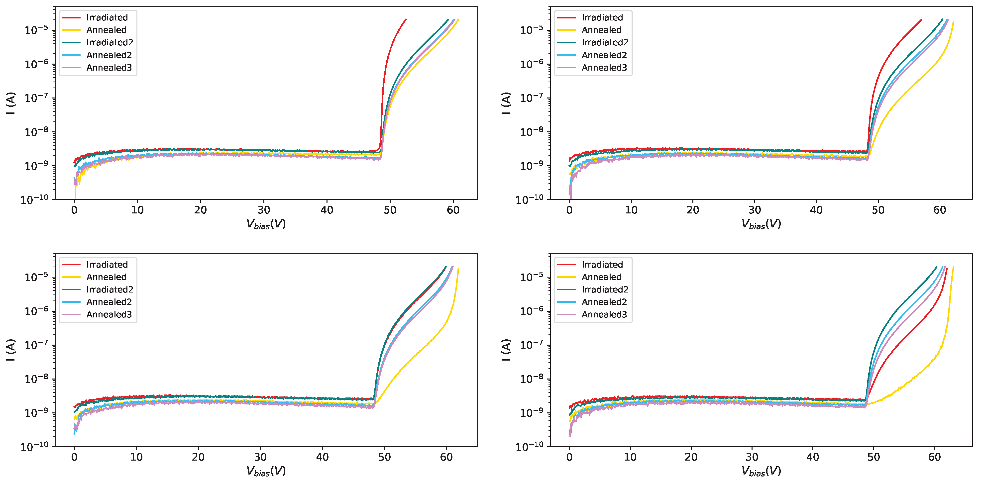
Figure 9.
IV-curves at −35 °C: in red after first irradiation, in yellow after first annealing, in teal after the second irradiation campaign, in light blue after second annealing and in magenta after third annealing; SiPM # 0 on (top left), SiPM # 3 on (top right), SiPM # 5 on (bottom left), SiPM # 7 on (bottom right).
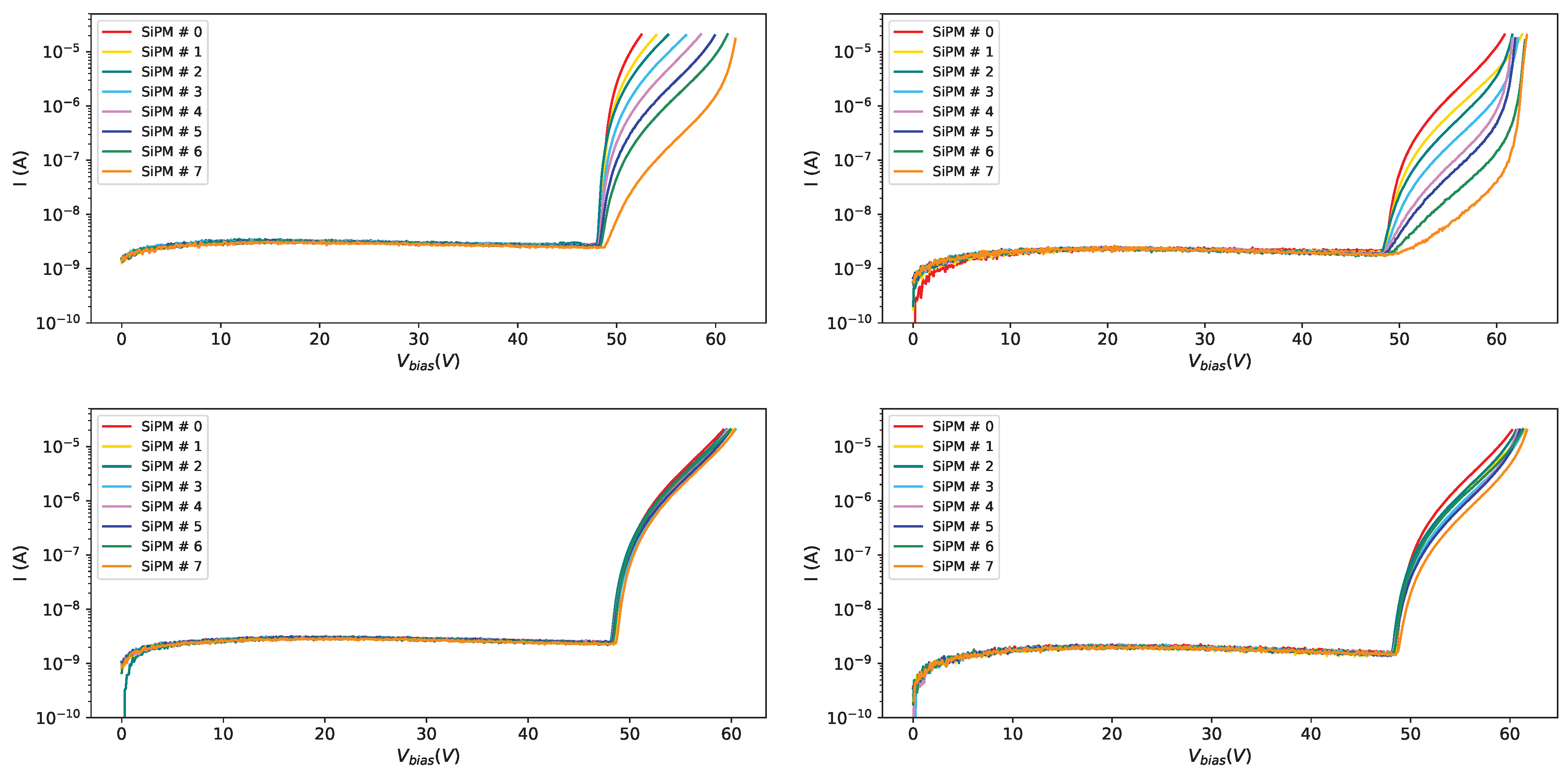
Figure 10.
IV-curves at −35 °C for set H1: after first irradiation (top left), after first annealing (top right), after second irradiation (bottom left) and after third annealing (bottom right).
Figure 10.
IV-curves at −35 °C for set H1: after first irradiation (top left), after first annealing (top right), after second irradiation (bottom left) and after third annealing (bottom right).
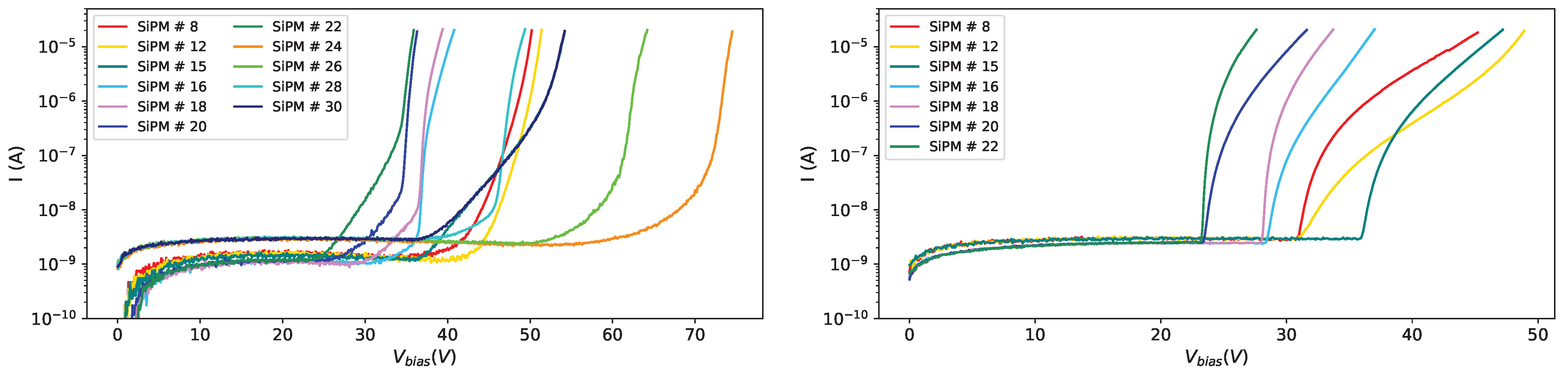
Figure 11.
IV-curves for SiPMs from different producers at temperature of 20 °C before irradiation (left) and after first irradiation at neq/cm2 (right).
Figure 11.
IV-curves for SiPMs from different producers at temperature of 20 °C before irradiation (left) and after first irradiation at neq/cm2 (right).
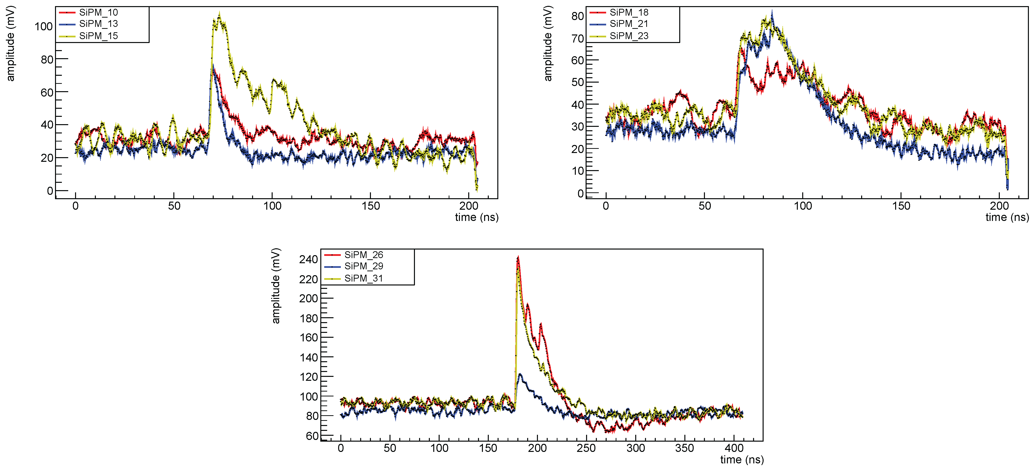
Figure 12.
Waveforms before irradiation at 10 °C. Set FBK1 (top left): red for SiPM , blue for SiPM , yellow for SiPM . Set MIX1 (top right): red for SiPM , blue for SiPM , yellow for SiPM . Set H2 (bottom): red for SiPM , blue for SiPM , yellow for SiPM .
Figure 12.
Waveforms before irradiation at 10 °C. Set FBK1 (top left): red for SiPM , blue for SiPM , yellow for SiPM . Set MIX1 (top right): red for SiPM , blue for SiPM , yellow for SiPM . Set H2 (bottom): red for SiPM , blue for SiPM , yellow for SiPM .
Figure 13.
Time vs. amplitude for Hamamatsu SiPM before irradiation.
Figure 13.
Time vs. amplitude for Hamamatsu SiPM before irradiation.
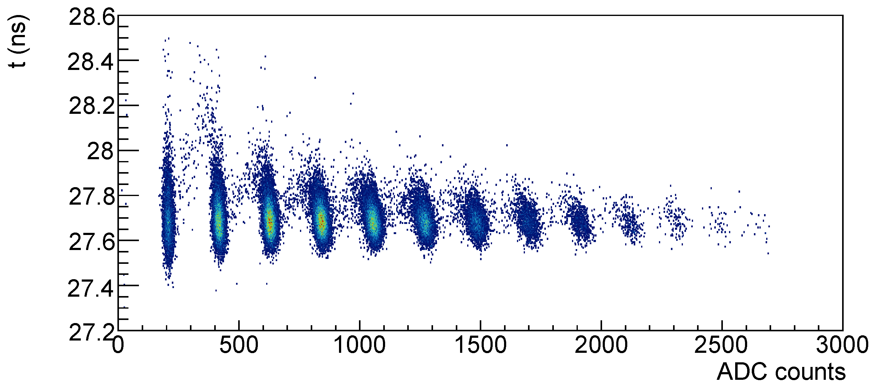
Figure 14.
Time vs. amplitude for single-photon signal (left) and for four-photons signal (right).
Figure 14.
Time vs. amplitude for single-photon signal (left) and for four-photons signal (right).
Figure 15.
Gain vs. (left) and vs. overvoltage (right) for all SiPMs of set H1 at T = −30 °C before irradiation.
Figure 15.
Gain vs. (left) and vs. overvoltage (right) for all SiPMs of set H1 at T = −30 °C before irradiation.
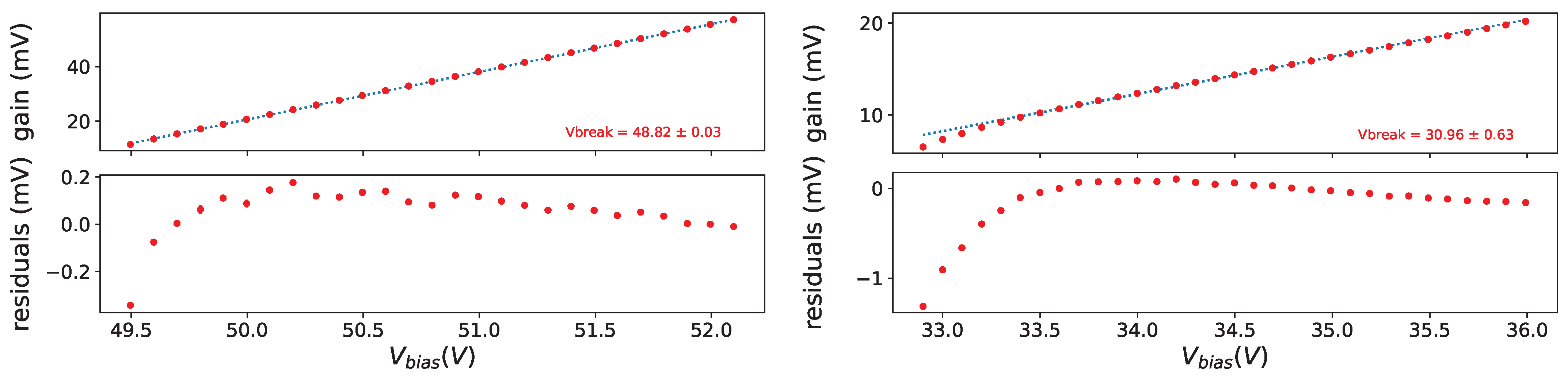
Figure 16.
Gain vs. for SiPM #7 (left) and #11 (right) at T = −30 °C before irradiation on (top), residuals of linear fit on (bottom).
Figure 16.
Gain vs. for SiPM #7 (left) and #11 (right) at T = −30 °C before irradiation on (top), residuals of linear fit on (bottom).
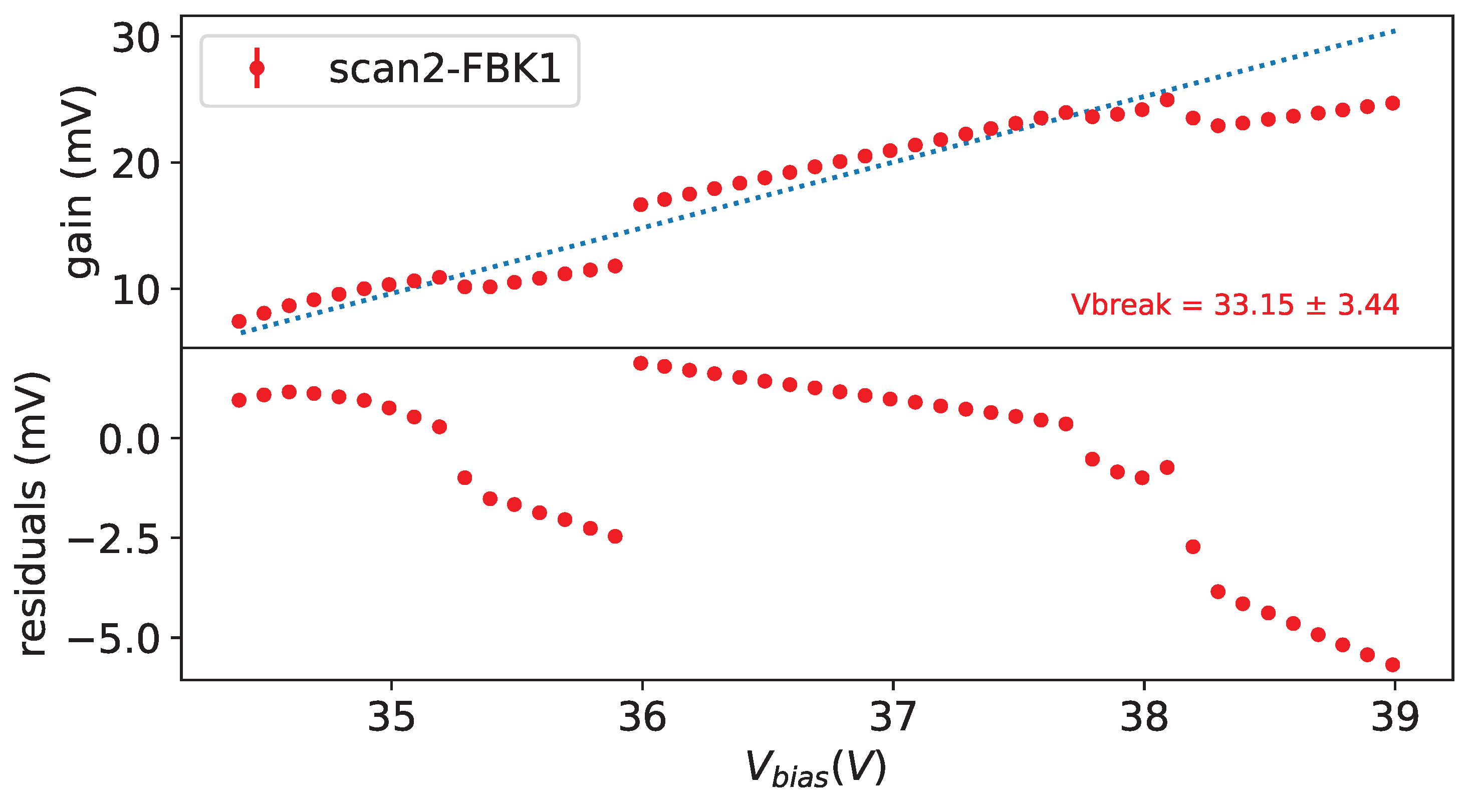
Figure 17.
Expanded view of IV-curve for SiPM at −30 °C: the teal vertical line shows the breakdown voltage obtained from the gain vs. bias voltage fit.
Figure 17.
Expanded view of IV-curve for SiPM at −30 °C: the teal vertical line shows the breakdown voltage obtained from the gain vs. bias voltage fit.
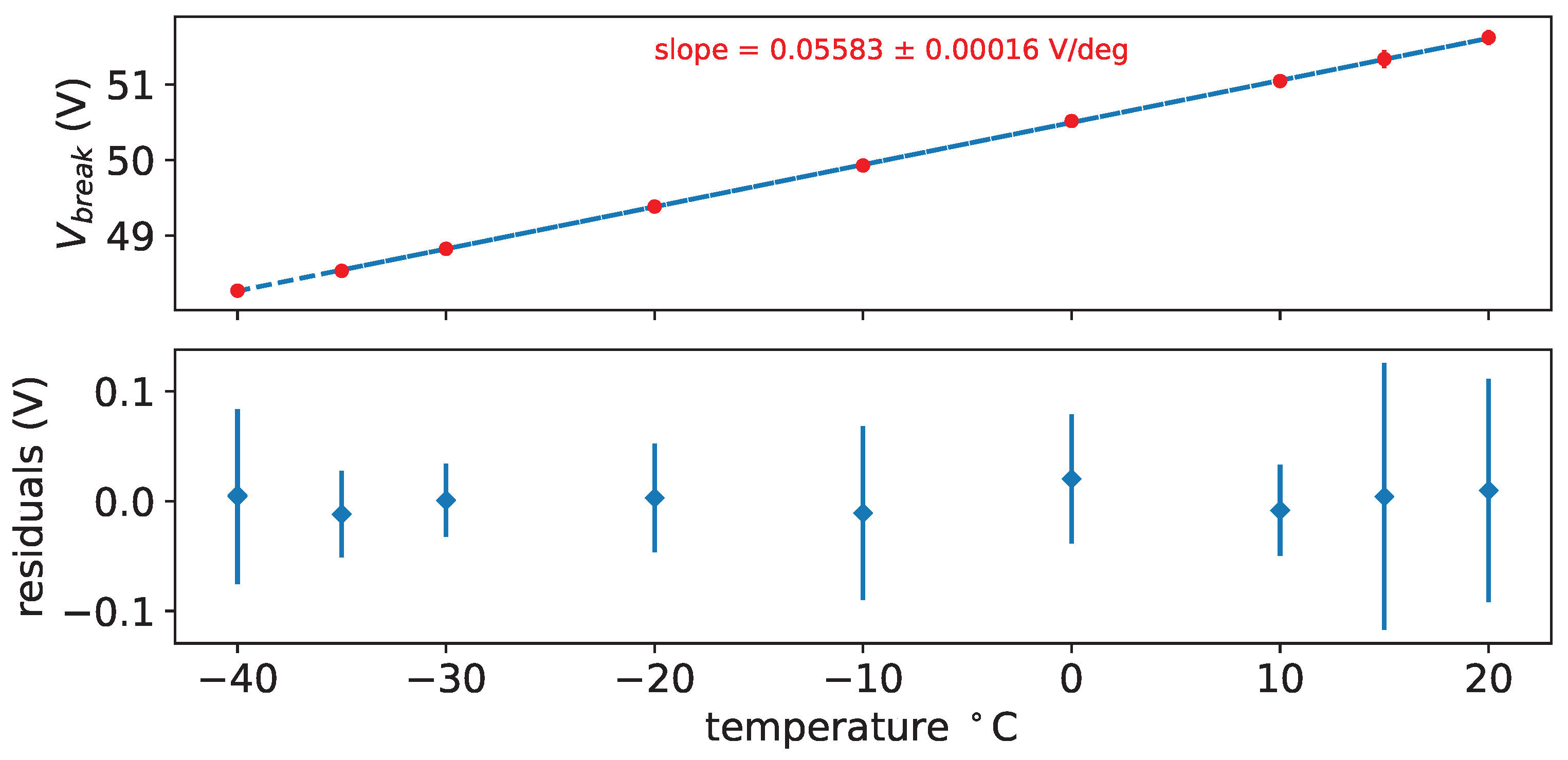
Figure 18.
Breakdown voltage (V) vs. temperature for SiPM # 7 before irradiation. In the bottom plot residuals of the fit are shown.
Figure 18.
Breakdown voltage (V) vs. temperature for SiPM # 7 before irradiation. In the bottom plot residuals of the fit are shown.
Figure 19.
Slope vs. temperature for SiPMs of set H1.
Figure 19.
Slope vs. temperature for SiPMs of set H1.
Figure 20.
Gain vs. for SiPM FBK before irradiation at T = 10 °C. On the top plot the blue dots show the interpolated line.
Figure 20.
Gain vs. for SiPM FBK before irradiation at T = 10 °C. On the top plot the blue dots show the interpolated line.
Figure 21.
Gain vs. for SiPM FBK at T = −35 °C, before first irradiation (red), after first irradiation (orange), after annealing (teal) and after second irradiation (blue).
Figure 21.
Gain vs. for SiPM FBK at T = −35 °C, before first irradiation (red), after first irradiation (orange), after annealing (teal) and after second irradiation (blue).
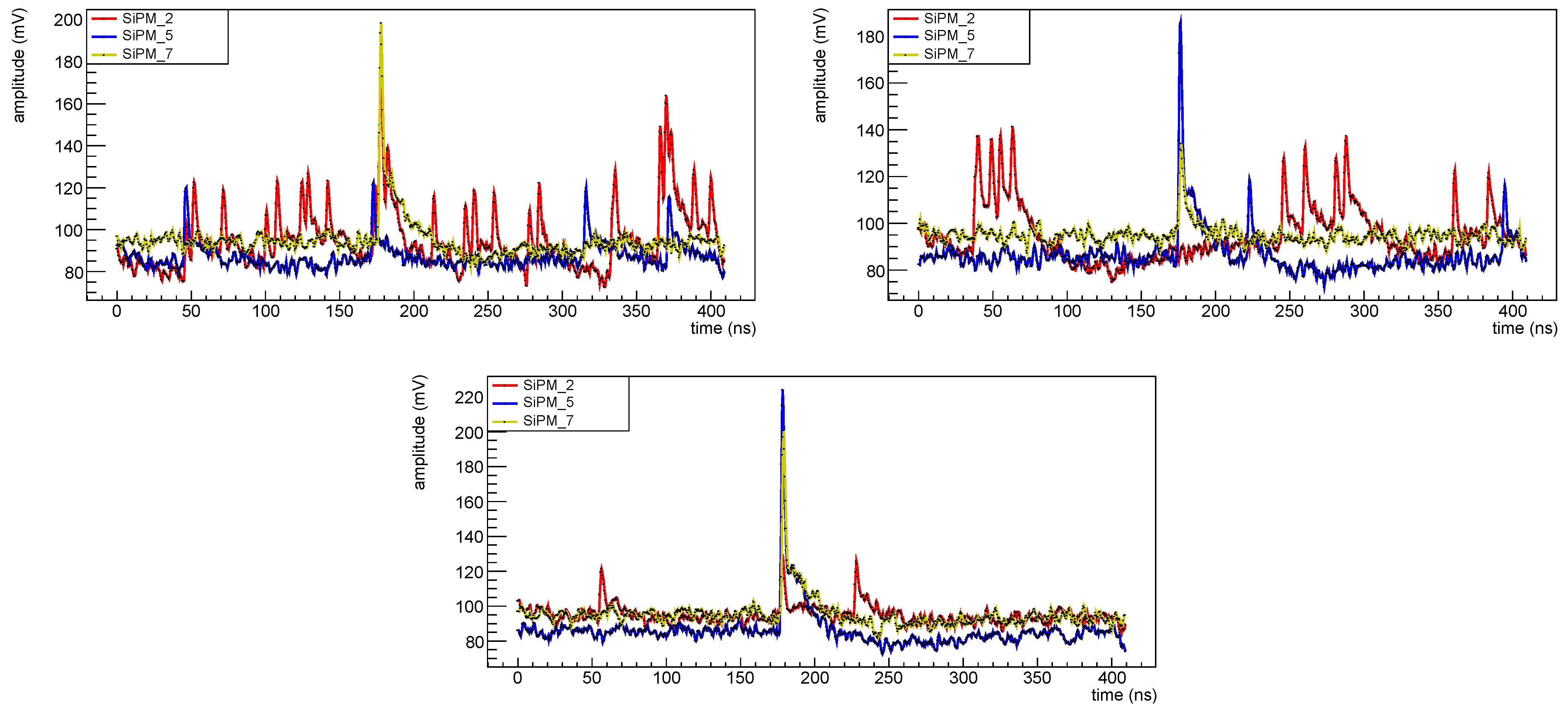
Figure 22.
Waveforms for SiPM # 2 (red), 5 (blue) and 7 (yellow), of set H1, after first irradiation campaign: on the (top left) at 10 °C, on the (top right) at −10 °C and on the (bottom) at −30 °C. These waveforms were taken all at an overvoltage of 2 V.
Figure 22.
Waveforms for SiPM # 2 (red), 5 (blue) and 7 (yellow), of set H1, after first irradiation campaign: on the (top left) at 10 °C, on the (top right) at −10 °C and on the (bottom) at −30 °C. These waveforms were taken all at an overvoltage of 2 V.
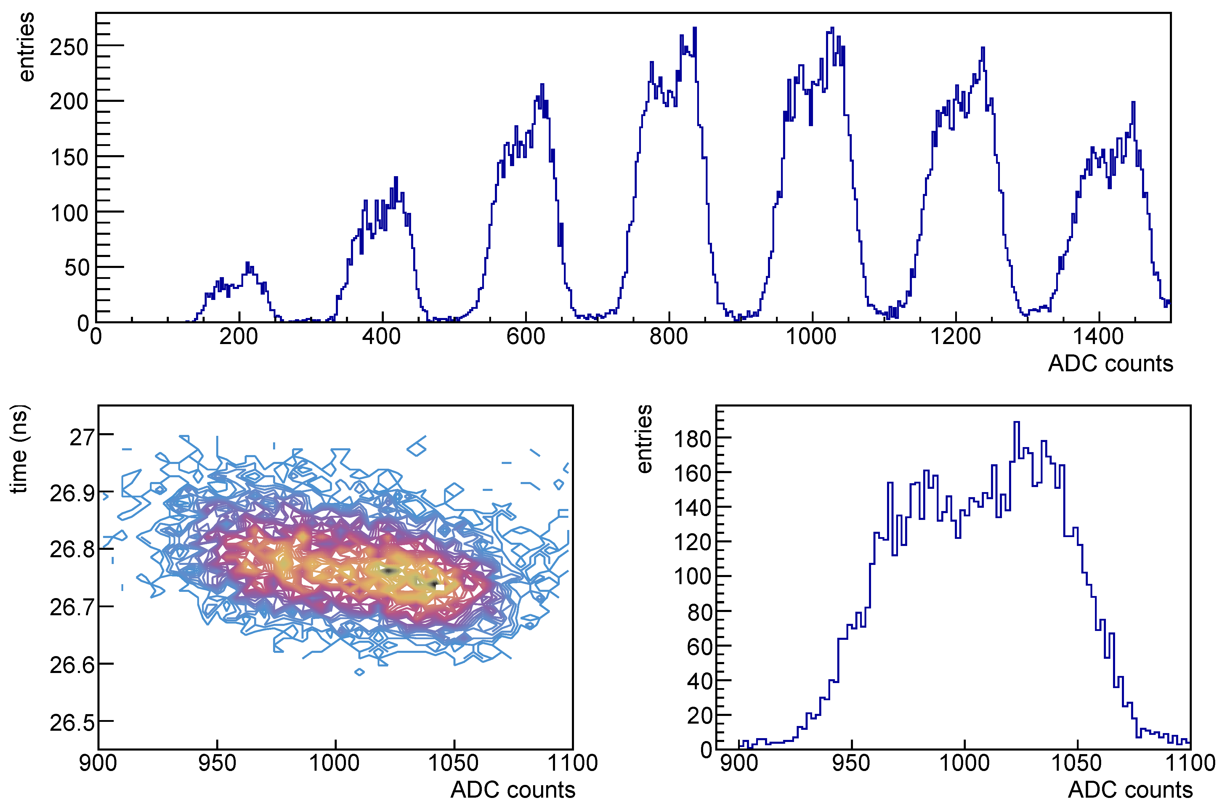
Figure 23.
SiPM at 0 °C: on (top) amplitude spectrum, on (bottom) plots relative to the five photon signal: on the (left) the time vs. amplitude and on the (right) the amplitude.
Figure 23.
SiPM at 0 °C: on (top) amplitude spectrum, on (bottom) plots relative to the five photon signal: on the (left) the time vs. amplitude and on the (right) the amplitude.
Figure 24.
Time vs. amplitude distributions for SiPM # 4 at 20 °C in blue and at −30 °C in red. Both distributions are taken at the same overvoltage.
Figure 24.
Time vs. amplitude distributions for SiPM # 4 at 20 °C in blue and at −30 °C in red. Both distributions are taken at the same overvoltage.
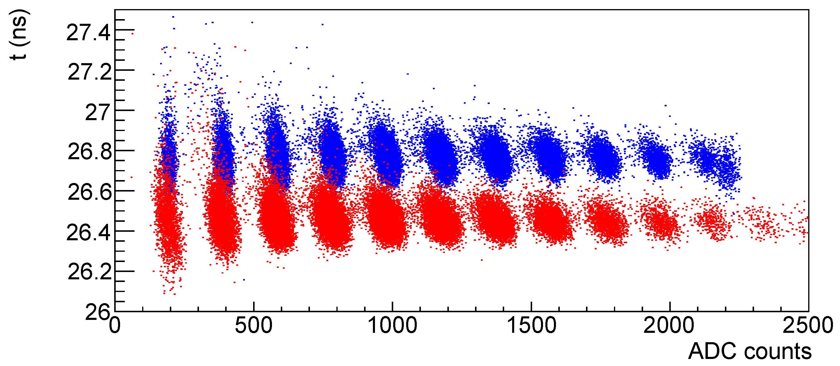
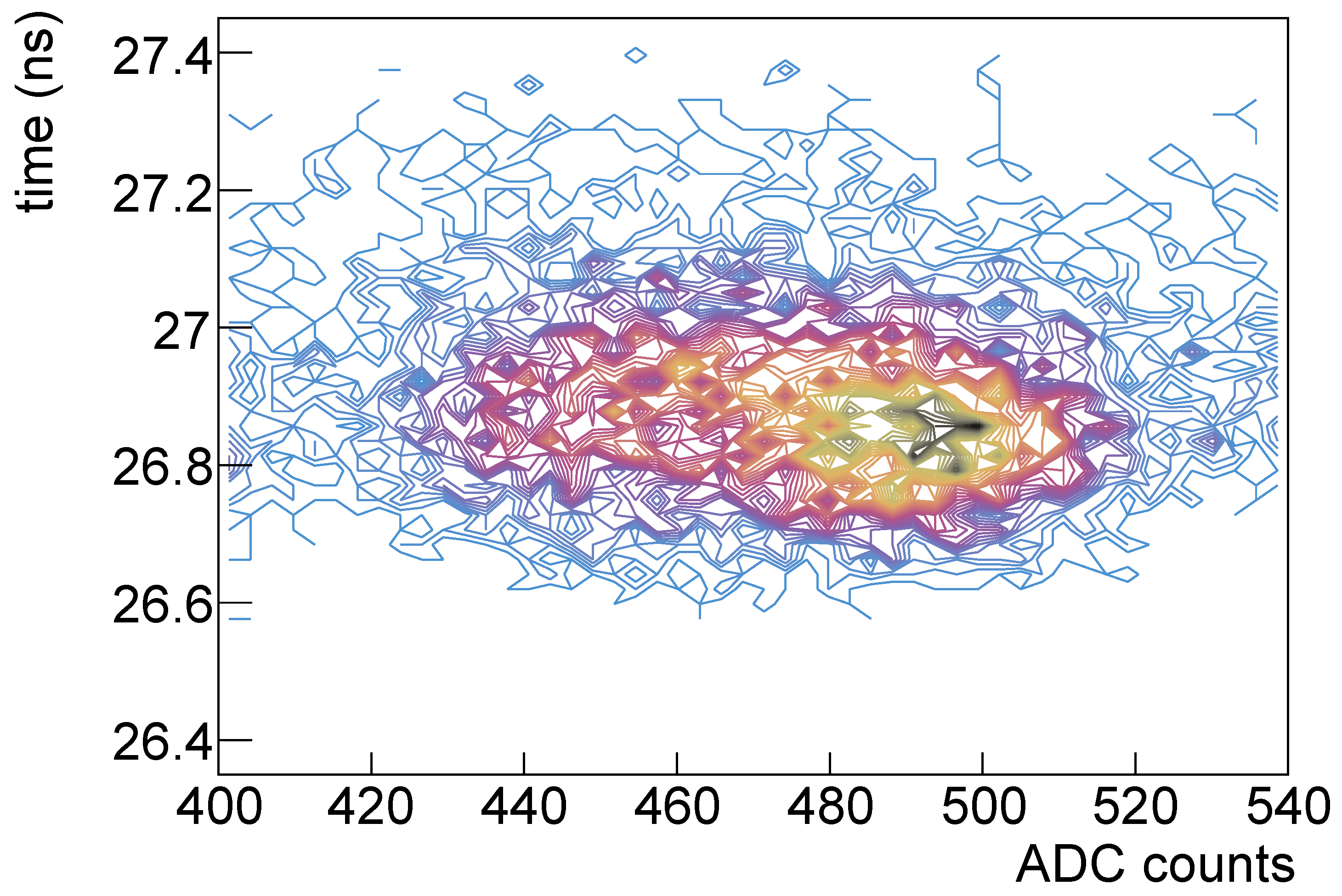
Figure 25.
SiPM at 0 °C: time (ns) vs. amplitude (ADC).
Figure 25.
SiPM at 0 °C: time (ns) vs. amplitude (ADC).
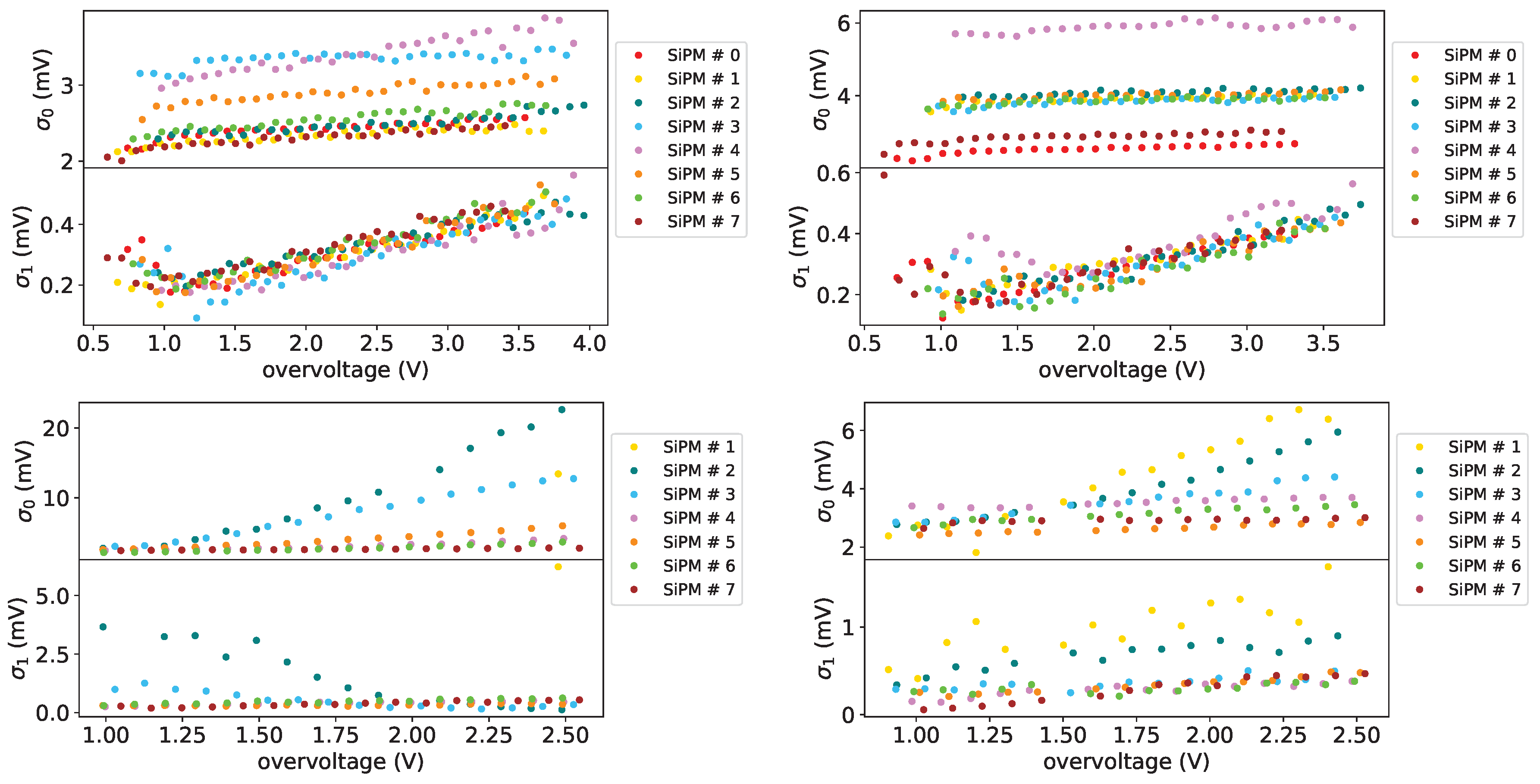
Figure 26.
Photon peak width parameters for device set H1, top plots before irradiation, at 10 °C on the (left) and −20 °C on the (right); bottom plots after first irradiation, at 10 °C on the (left) and −20 °C on the (right). On (top) panel the constant term , on (bottom) panel the variable term .
Figure 26.
Photon peak width parameters for device set H1, top plots before irradiation, at 10 °C on the (left) and −20 °C on the (right); bottom plots after first irradiation, at 10 °C on the (left) and −20 °C on the (right). On (top) panel the constant term , on (bottom) panel the variable term .
Figure 27.
Photon peak widths parameters (in mV) for SiPM #12 (set FBK1) as a function of the overvoltage (in V) for different temperatures: on the (top left) before irradiation, on the (top right) after first irradiation on the (bottom) after first annealing. On top panel the constant term, on bottom panel the variable term.
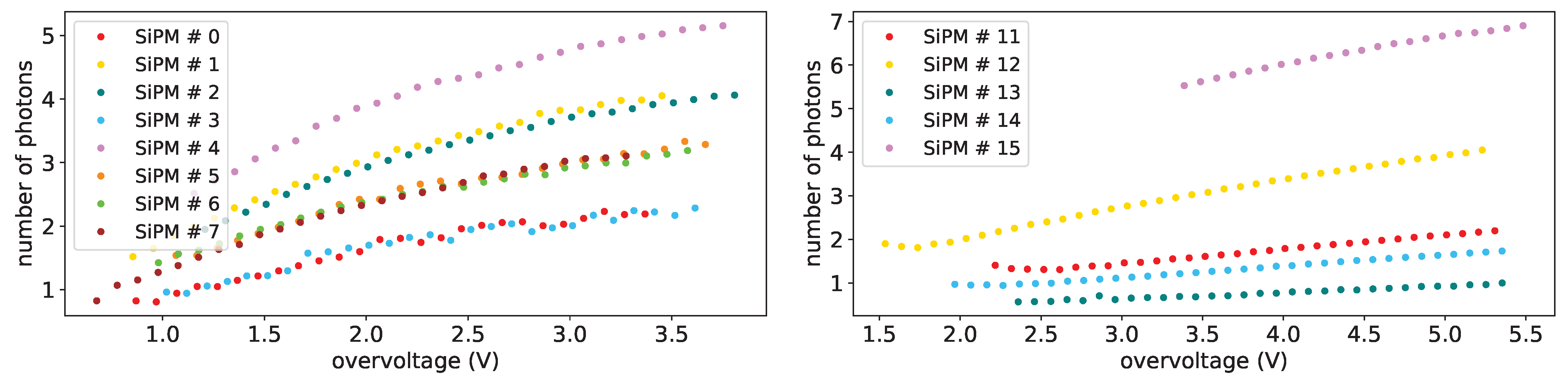
Figure 28.
Average number of photons vs. overvoltage at T = −30 °C before irradiation for H1 set on lef and set FBK1 on (right).
Figure 28.
Average number of photons vs. overvoltage at T = −30 °C before irradiation for H1 set on lef and set FBK1 on (right).
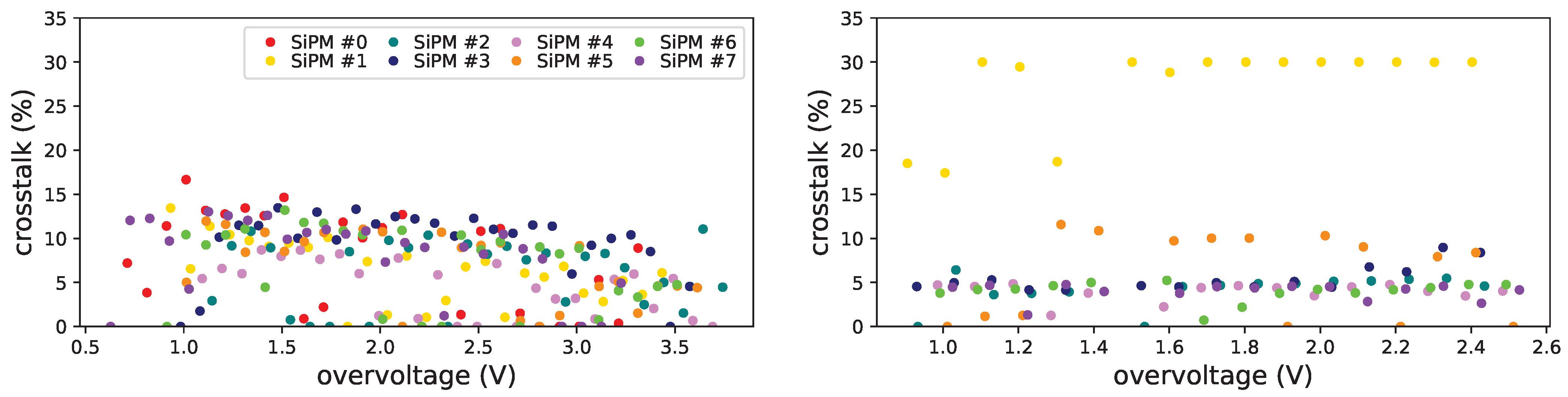
Figure 29.
Prompt crosstalk vs. overvoltage for SiPMs of set H1 at −20 °C, before irradiation (left), after irradiation (right). Data could not be extracted after irradiation for SiPM at this temperature. The legend is the same for the two plots. Zero values come from unreliable fits.
Figure 29.
Prompt crosstalk vs. overvoltage for SiPMs of set H1 at −20 °C, before irradiation (left), after irradiation (right). Data could not be extracted after irradiation for SiPM at this temperature. The legend is the same for the two plots. Zero values come from unreliable fits.
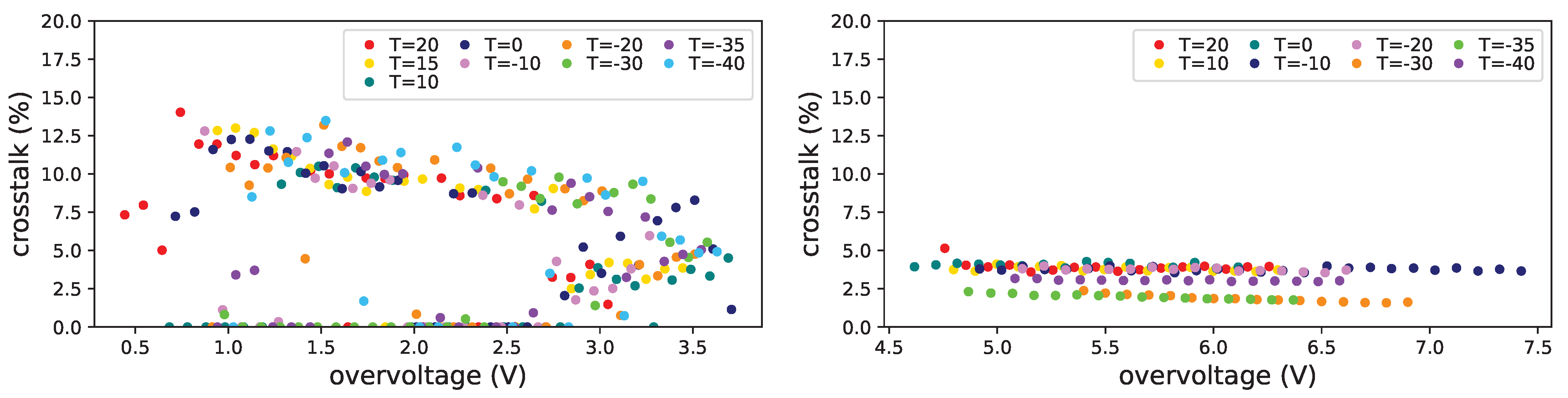
Figure 30.
Prompt crosstalk as a function of overvoltage at different temperatures for Hamamatsu SiPM (left) and for FBK (right) before irradiation. Zero values come from unreliable fits.
Figure 30.
Prompt crosstalk as a function of overvoltage at different temperatures for Hamamatsu SiPM (left) and for FBK (right) before irradiation. Zero values come from unreliable fits.
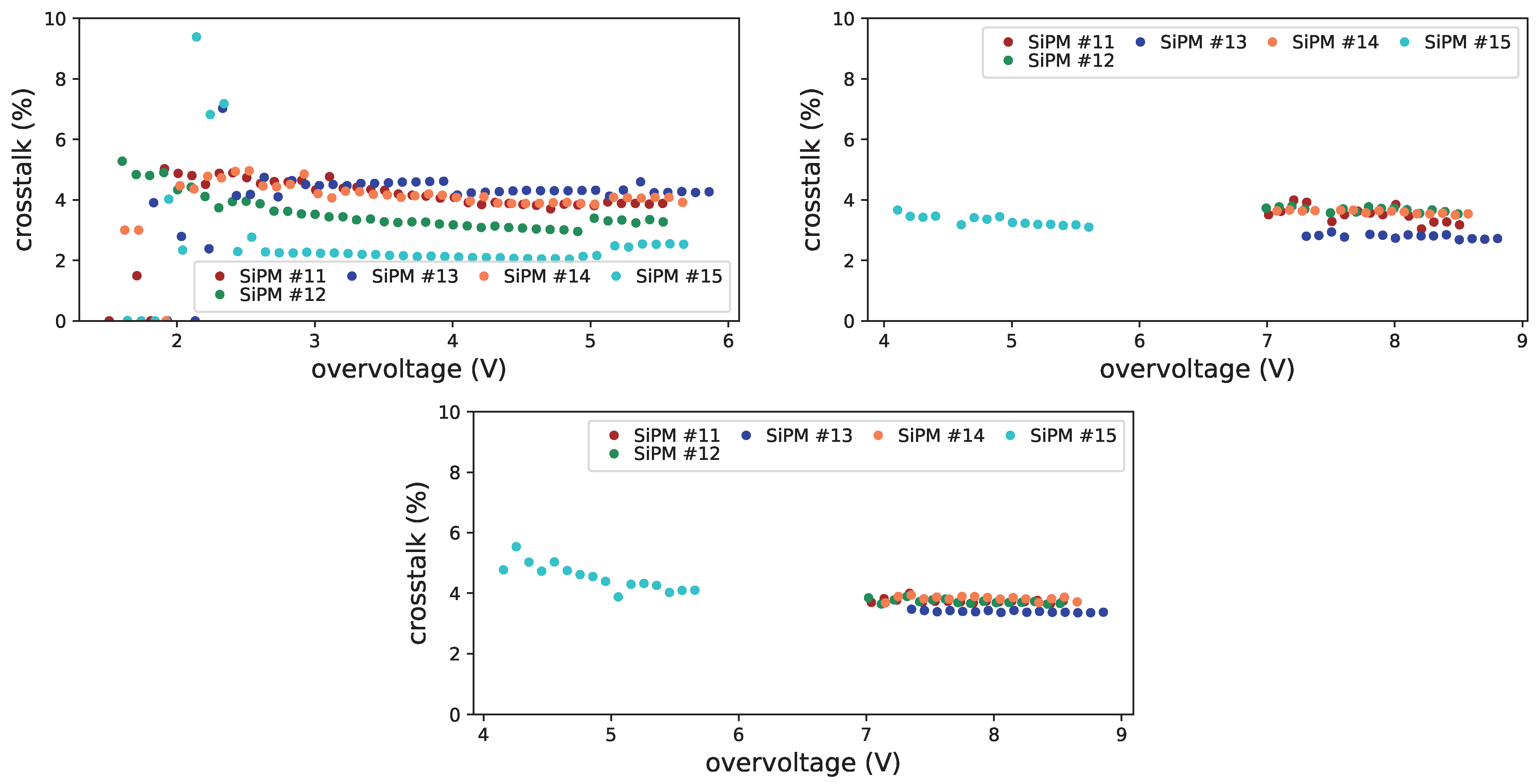
Figure 31.
Prompt crosstalk vs. overvoltage for FBK1 SiPMs at −20 °C, before irradiation (top left), after first irradiation (top right) and after first annealing (bottom). Zero values come from unreliable fits.
Figure 31.
Prompt crosstalk vs. overvoltage for FBK1 SiPMs at −20 °C, before irradiation (top left), after first irradiation (top right) and after first annealing (bottom). Zero values come from unreliable fits.
Figure 32.
Time distributions for one photon (left) two photon (center) and more than two photon signals. The distribution is fitted with two gaussian distributions: in red the global fit, in blue and green the two gaussian contributions are shown. Distributions obtained for SiPM at an overvoltage of 2 V and at 0 °C before irradiation.
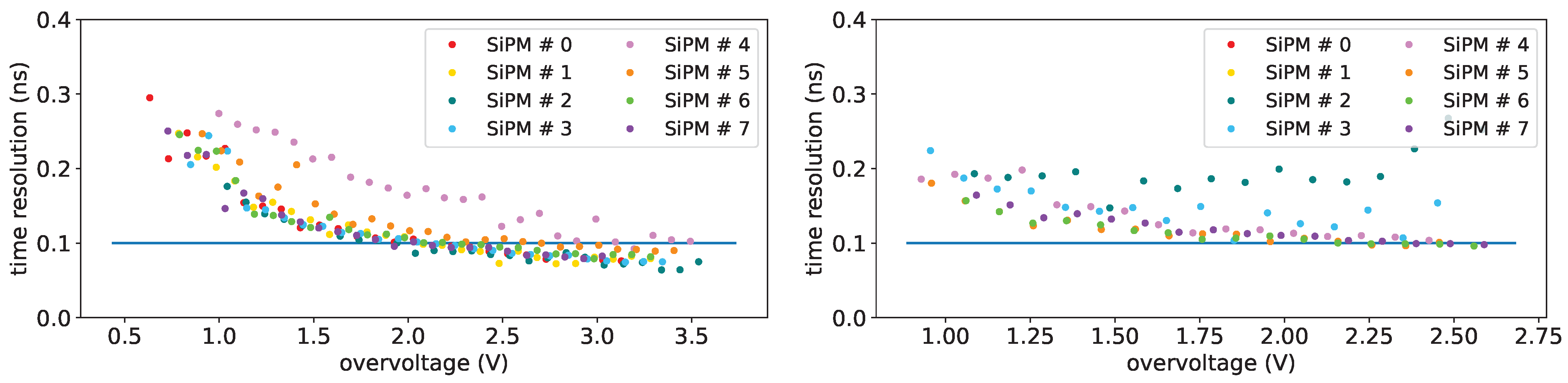
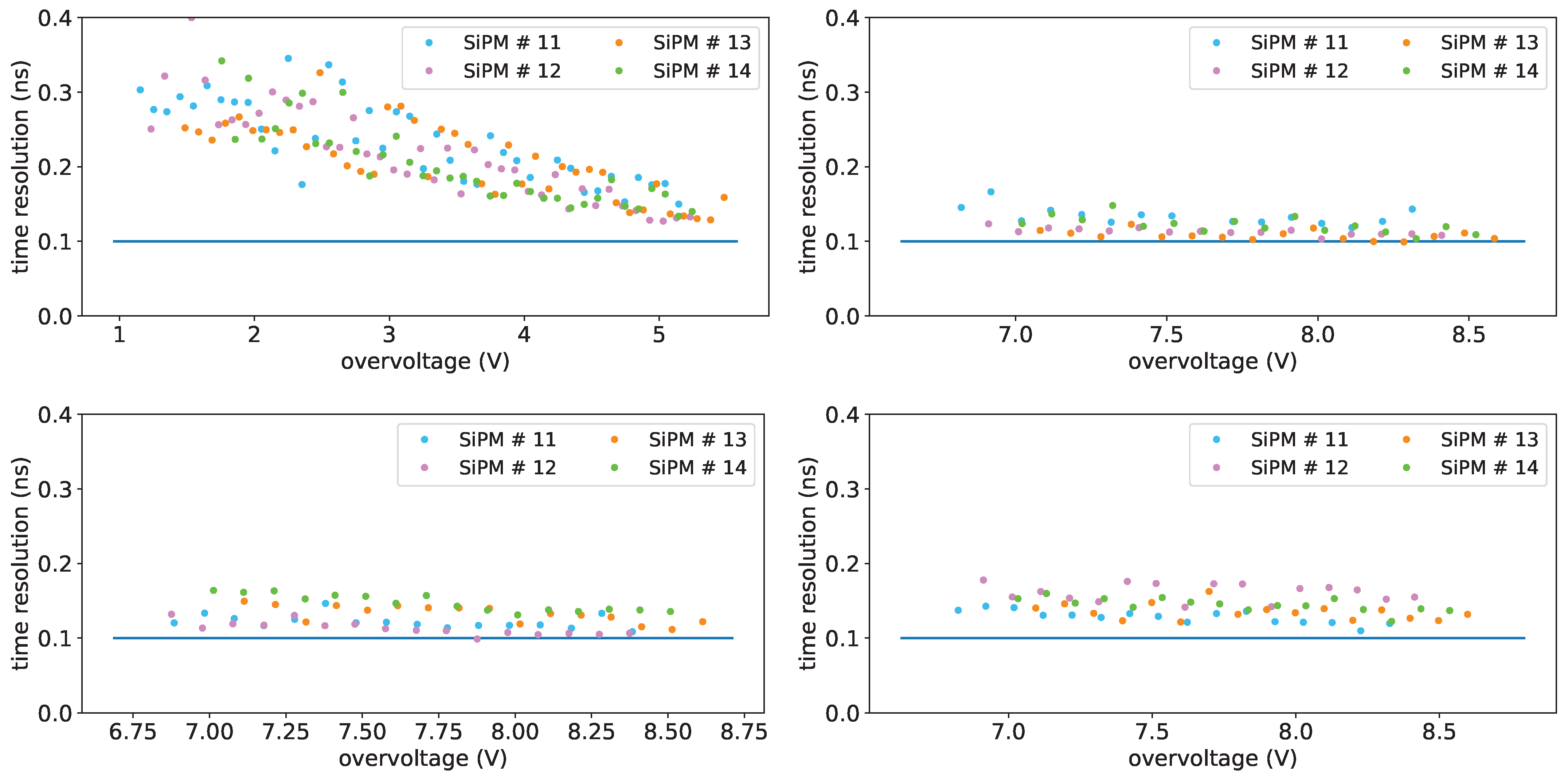
Figure 33.
Single-photon time resolution vs. overvoltage for set H1 at a temperature of −10 °C before irradiation on (left) and after on (right). Horizontal line: reference for 100 ps.
Figure 33.
Single-photon time resolution vs. overvoltage for set H1 at a temperature of −10 °C before irradiation on (left) and after on (right). Horizontal line: reference for 100 ps.
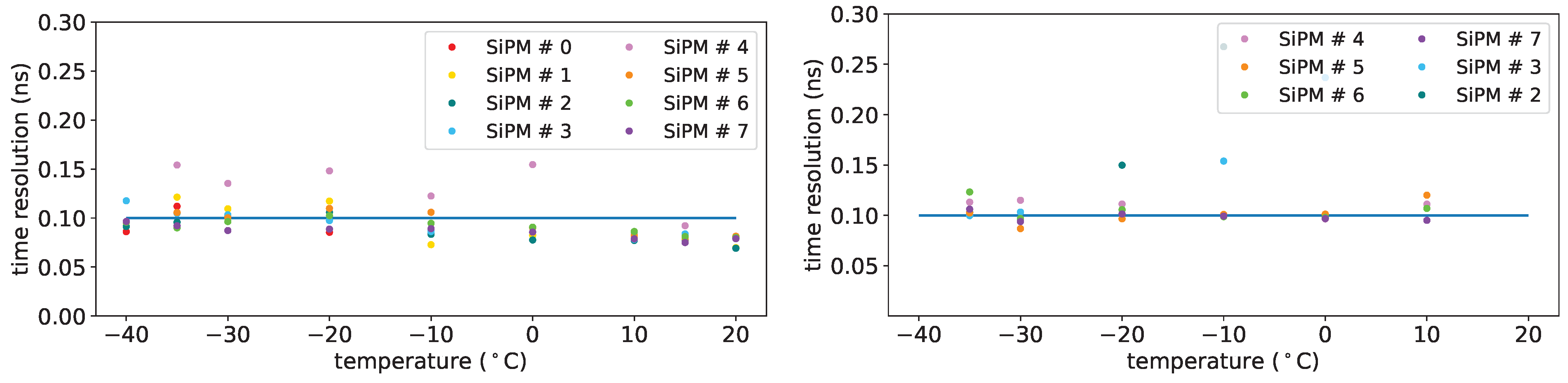
Figure 34.
Single-photon time resolution vs. temperature for set H1 at an overvoltage of 2.5 V before on (left) and after on (right) first irradiation. Horizontal line: reference for 100 ps.
Figure 34.
Single-photon time resolution vs. temperature for set H1 at an overvoltage of 2.5 V before on (left) and after on (right) first irradiation. Horizontal line: reference for 100 ps.
Figure 35.
Single-photon time sigma vs. overvoltage for FBK devices of set FBK1 at a temperature of −30 °C. Before irradiation on (top left), after first irradiation on (bottom left), after first annealing on (top right) and after second irradiation on (bottom right). Horizontal scales are not the same: after first data taking the overvoltage range was moved upwards. Horizontal line: reference for 100 ps.
Figure 36.
Single-photon time sigma for FBK devices before irradiation (top left, overvoltage 5 V), after first irradiation (top right, overvoltage 8 V), after first annealing (bottom left, overvoltage 8 V) and after second irradiation (bottom right, overvoltage 8 V). Horizontal line: reference for 100 ps.
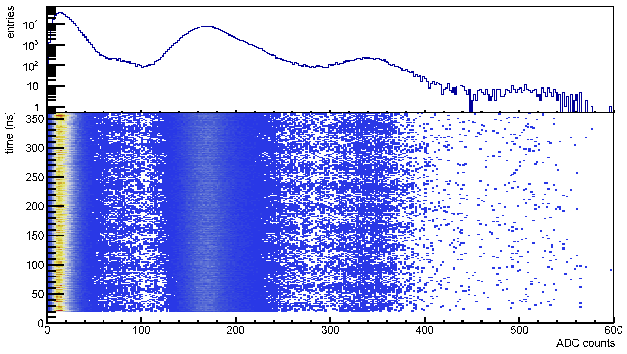
Figure 37.
Dark count rate plots: on (top) amplitude spectra (ADC counts), on (bottom) the scatter plot of the signal time (ns) vs. the amplitude.
Figure 37.
Dark count rate plots: on (top) amplitude spectra (ADC counts), on (bottom) the scatter plot of the signal time (ns) vs. the amplitude.
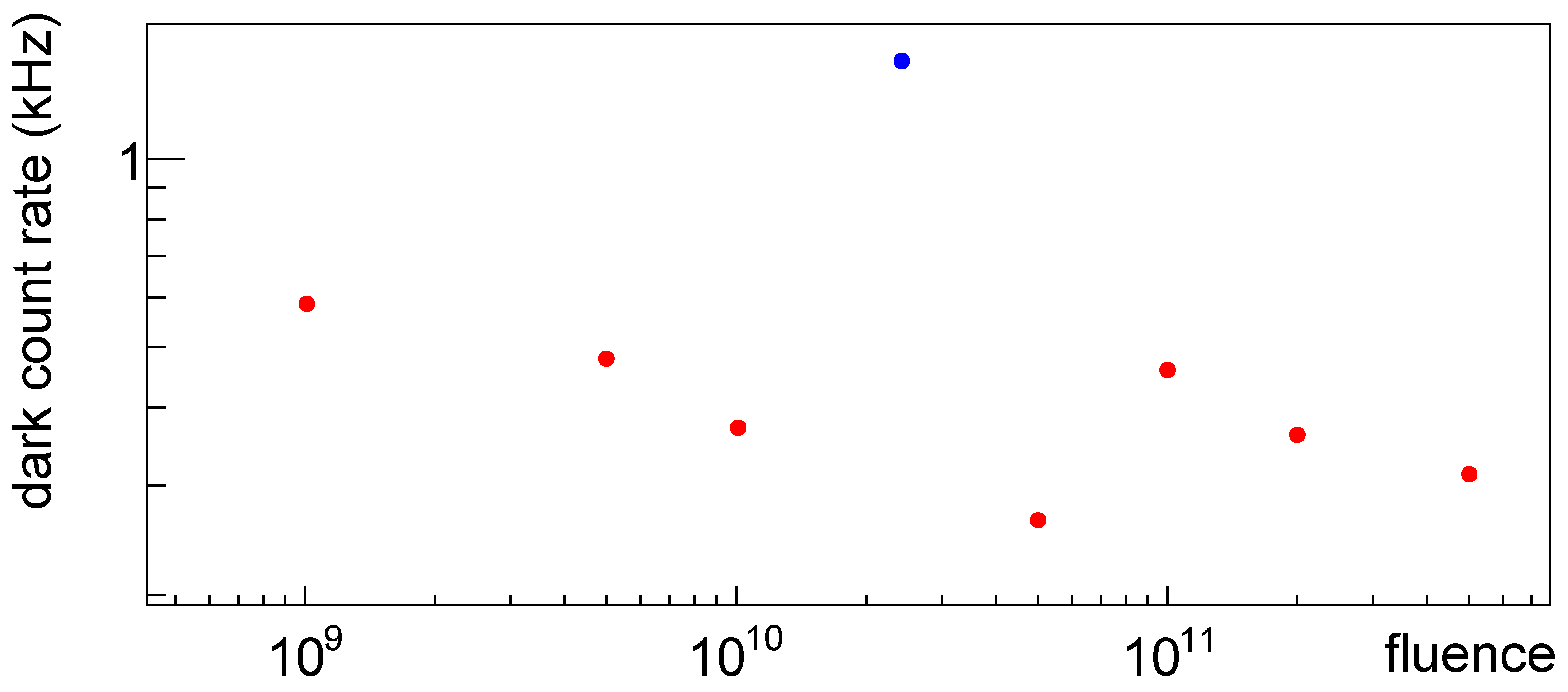
Figure 38.
Dark count rate for SiPMs of set H1 at −20 °C and at an overvoltage of 2 V plotted vs. fluence of first irradiation. In blue DCR for SiPM , in red for the others.
Figure 38.
Dark count rate for SiPMs of set H1 at −20 °C and at an overvoltage of 2 V plotted vs. fluence of first irradiation. In blue DCR for SiPM , in red for the others.
Figure 39.
Dark count rate for SiPM set H1 plotted vs. fluence of first irradiation at various temperatures.
Figure 39.
Dark count rate for SiPM set H1 plotted vs. fluence of first irradiation at various temperatures.
Figure 40.
Dark count rate for SiPMs of set H1 plotted vs. fluence of first irradiation at −20 °C before irradiation at an overvoltage of 2 V. In blue DCR for SiPM , in red for the others.
Figure 40.
Dark count rate for SiPMs of set H1 plotted vs. fluence of first irradiation at −20 °C before irradiation at an overvoltage of 2 V. In blue DCR for SiPM , in red for the others.
Figure 41.
Dark count rate for SiPM plotted vs. temperature after first irradiation at an overvoltage of 2 V. Rates in linear scale on top, in log10 scale on bottom.
Figure 41.
Dark count rate for SiPM plotted vs. temperature after first irradiation at an overvoltage of 2 V. Rates in linear scale on top, in log10 scale on bottom.
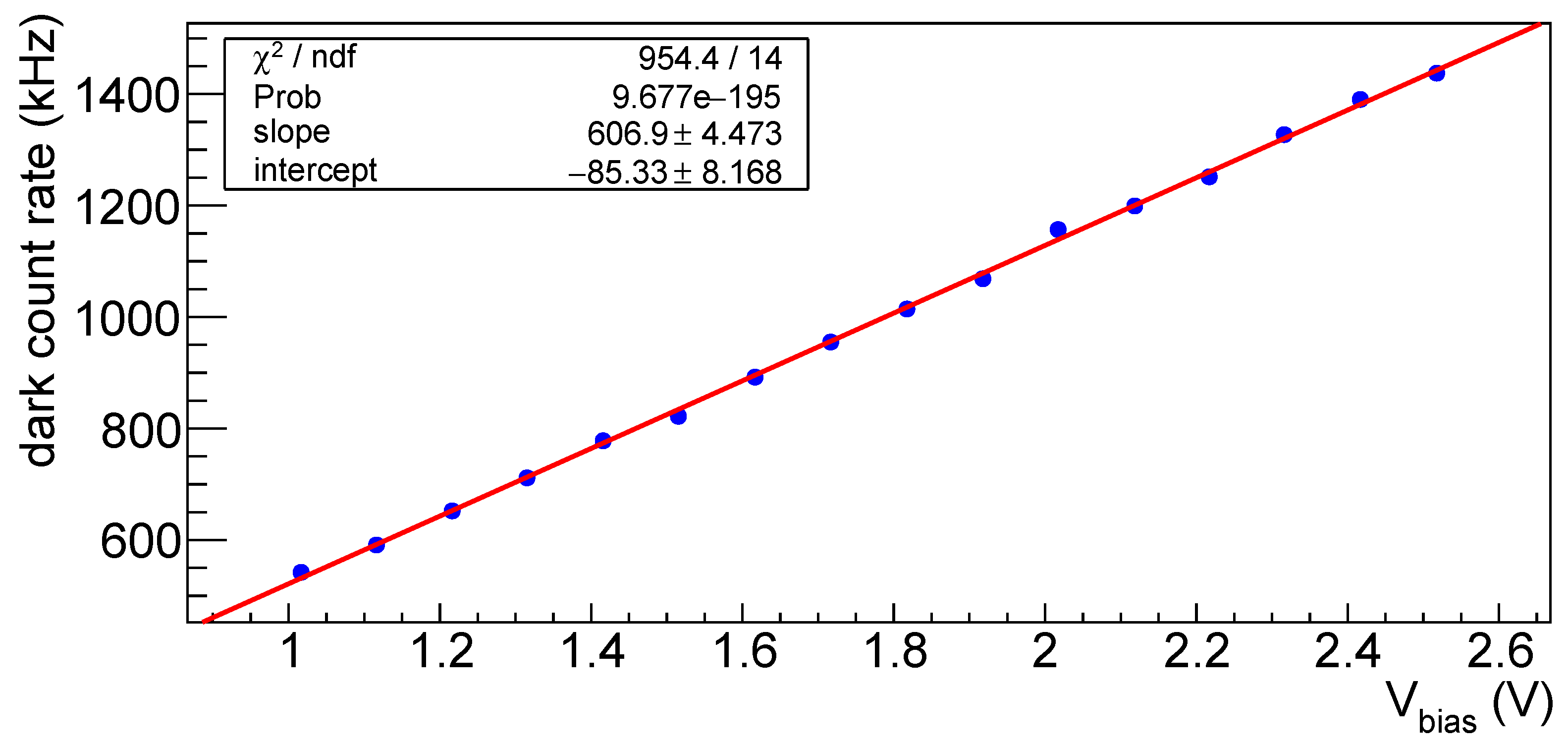
Figure 42.
Dark count rate for SiPM vs. overvoltage after first irradiation at t = −20 °C. In the box on top left of the plot the results of the linear fit are shown as an example.
Figure 42.
Dark count rate for SiPM vs. overvoltage after first irradiation at t = −20 °C. In the box on top left of the plot the results of the linear fit are shown as an example.
Table 1.
SiPM sets.
| Set | ID | Model | Set | ID | Model |
|---|
| H1 | 0 | Hamamatsu S13360-1350PE | MIX1 | 16 | Ketek PM3315-WL |
| 1 | Hamamatsu S13360-1350PE | 17 | Ketek PM3315-WL |
| 2 | Hamamatsu S13360-1350PE | 18 | Ketek PM3335-WL |
| 3 | Hamamatsu S13360-1350PE | 19 | Ketek PM3335-WL |
| 4 | Hamamatsu S13360-1350PE | 20 | OnSemi 10035 |
| 5 | Hamamatsu S13360-1350PE | 21 | OnSemi 10035 |
| 6 | Hamamatsu S13360-1350PE | 22 | OnSemi 30035 |
| 7 | Hamamatsu S13360-1350PE | 23 | OnSemi 30035 |
| FBK1 | 8 | FBK NUV-HD-RH-3015 | H2 | 24 | Hamamatsu S13360-3025PE |
| 9 | FBK NUV-HD-RH-3015 | 25 | Hamamatsu S13360-3025PE |
| 10 | FBK NUV-HD-RH-3015 | 26 | Hamamatsu S13360-3050PE |
| 11 | FBK NUV-HD-RH-1015 | 27 | Hamamatsu S13360-3050PE |
| 12 | FBK NUV-HD-RH-1015 | 28 | Hamamatsu S14160-3015PS |
| 13 | FBK NUV-HD-RH-1015 | 29 | Hamamatsu S14160-3015PS |
| 14 | FBK NUV-HD-RH-1015 | 30 | Hamamatsu S14160-3050HS |
| 15 | Hamamatsu S14160-3050HS | 31 | Hamamatsu S14160-3050HS |
Table 2.
SiPM geometrical characteristics.
Table 2.
SiPM geometrical characteristics.
| Model | Size (mm2) | Pixel (μm) |
|---|
| Hamamatsu S13360-1350PE | | 50 |
| Hamamatsu S14160-3050HS | | 50 |
| Hamamatsu S13360-3050PE | | 50 |
| Hamamatsu S13360-3025PE | | 25 |
| Hamamatsu S14160-3015PS | | 15 |
| Ketek PM3315-WL | | 15 |
| Ketek PM3335-WL | | 35 |
| OnSemi 10035 | | 35 |
| OnSemi 30035 | | 35 |
| FBK NUV-HD-RH-1015 | | 15 |
| FBK NUV-HD-RH-3015 | | 15 |
Table 3.
Integrated neutron fluences (neq/cm2) for SiPMs of set H1 obtained in the two irradiation campaigns.
Table 3.
Integrated neutron fluences (neq/cm2) for SiPMs of set H1 obtained in the two irradiation campaigns.
| SiPM ID | November 2022 | April 2024 |
|---|
| 0 | 5.07 × 10¹¹ | 9.97 × 10⁹ |
| 1 | 2.03 × 10¹¹ | 1.01 × 10¹⁰ |
| 2 | 1.01 × 10¹¹ | 1.00 × 10¹⁰ |
| 3 | 5.07 × 10¹⁰ | 9.99 × 10⁹ |
| 4 | 2.45 × 10¹⁰ | 9.99 × 10⁹ |
| 5 | 1.02 × 10¹⁰ | 9.99 × 10⁹ |
| 6 | 5.06 × 10⁹ | 1.00 × 10¹⁰ |
| 7 | 1.03 × 10⁹ | 1.00 × 10¹⁰ |
Table 4.
Integrated neutron fluences (neq/cm2) for SiPMs of set FBK1 obtained in the two irradiation campaigns.
Table 4.
Integrated neutron fluences (neq/cm2) for SiPMs of set FBK1 obtained in the two irradiation campaigns.
| SiPM ID | July 2023 | April 2024 |
|---|
| 8 | 1.01 × 10¹⁰ | 9.99 × 10⁹ |
| 9 | 4.98 × 10⁹ | 1.00 × 10¹⁰ |
| 10 | 1.01 × 10⁹ | 1.00 × 10¹⁰ |
| 11 | 2.00 × 10¹⁰ | 9.99 × 10⁹ |
| 12 | 1.00 × 10¹⁰ | 9.99 × 10⁹ |
| 13 | 5.00 × 10⁹ | 1.00 × 10¹⁰ |
| 14 | 1.04 × 10⁹ | 1.00 × 10¹⁰ |
| 15 | 9.94 × 10⁸ | 1.00 × 10¹⁰ |
Table 5.
Integrated neutron fluences (neq/cm2) for SiPMs of set MIX1 obtained in the two irradiation campaigns.
Table 5.
Integrated neutron fluences (neq/cm2) for SiPMs of set MIX1 obtained in the two irradiation campaigns.
| SiPM ID | July 2023 | April 2024 |
|---|
| 16 | 1.00 × 10¹⁰ | 1.01 × 10¹⁰ |
| 17 | 1.03 × 10⁹ | 1.00 × 10¹⁰ |
| 18 | 1.00 × 10¹⁰ | 9.99 × 10⁹ |
| 19 | 1.00 × 10⁹ | 1.00 × 10¹⁰ |
| 20 | 1.00 × 10¹⁰ | 9.99 × 10⁹ |
| 21 | 1.12 × 10⁹ | 1.00 × 10¹⁰ |
| 22 | 1.00 × 10¹⁰ | 9.98 × 10⁹ |
| 23 | 1.05 × 10⁹ | 1.00 × 10¹⁰ |
Table 6.
Breakdown voltage (V) before first irradiation for SiPMs of set H1.
Table 6.
Breakdown voltage (V) before first irradiation for SiPMs of set H1.
| T (°C) | SiPM # 0 | SiPM # 1 | SiPM # 2 | SiPM # 3 | SiPM # 4 | SiPM # 5 | SiPM # 6 | SiPM # 7 |
|---|
| 20 | 51.54 ± 0.14 | 51.39 ± 0.24 | 51.14 ± 0.30 | 51.26 ± 0.23 | 51.12 ± 0.14 | 51.22 ± 0.22 | 51.32 ± 0.19 | 51.62 ± 0.10 |
| 15 | 51.24 ± 0.09 | 51.07 ± 0.09 | 50.76 ± 0.09 | 50.94 ± 0.07 | 50.80 ± 0.08 | 50.93 ± 0.05 | 51.01 ± 0.12 | 51.34 ± 0.12 |
| 10 | 50.94 ± 0.09 | 50.81 ± 0.29 | 50.51 ± 0.10 | 50.66 ± 0.12 | 50.51 ± 0.08 | 50.63 ± 0.11 | 50.74 ± 0.10 | 51.05 ± 0.04 |
| 0 | 50.42 ± 0.08 | 50.29 ± 0.04 | 49.97 ± 0.07 | 50.15 ± 0.03 | 50.02 ± 0.14 | 50.13 ± 0.06 | 50.22 ± 0.02 | 50.52 ± 0.06 |
| −10 | 49.84 ± 0.11 | 49.70 ± 0.07 | 49.38 ± 0.08 | 49.57 ± 0.06 | 49.44 ± 0.15 | 49.54 ± 0.06 | 49.63 ± 0.07 | 49.93 ± 0.08 |
| −20 | 49.29 ± 0.04 | 49.16 ± 0.05 | 48.85 ± 0.06 | 49.03 ± 0.03 | 48.90 ± 0.08 | 49.00 ± 0.01 | 49.09 ± 0.01 | 49.38 ± 0.05 |
| −30 | 48.73 ± 0.03 | 48.60 ± 0.10 | 48.29 ± 0.01 | 48.46 ± 0.05 | 48.29 ± 0.07 | 48.44 ± 0.03 | 48.52 ± 0.03 | 48.82 ± 0.03 |
| −35 | 48.44 ± 0.08 | 48.32 ± 0.02 | 48.00 ± 0.02 | 48.19 ± 0.02 | 48.05 ± 0.04 | 48.15 ± 0.05 | 48.24 ± 0.03 | 48.53 ± 0.04 |
| −40 | 48.16 ± 0.07 | 48.05 ± 0.04 | 47.73 ± 0.02 | 47.91 ± 0.03 | - | - | 47.96 ± 0.03 | 48.27 ± 0.03 |
Table 7.
Gain variation over bias voltage (mV/V) before first irradiation for SiPMS of set H1.
Table 7.
Gain variation over bias voltage (mV/V) before first irradiation for SiPMS of set H1.
| T (°C) | SiPM # 0 | SiPM # 1 | SiPM # 2 | SiPM # 3 | SiPM # 4 | SiPM # 5 | SiPM # 6 | SiPM # 7 |
|---|
| 20 | 16.66 ± 0.03 | 16.58 ± 0.05 | 17.64 ± 0.07 | 18.24 ± 0.06 | 16.89 ± 0.03 | 17.66 ± 0.05 | 17.56 ± 0.05 | 17.69 ± 0.02 |
| 15 | 16.46 ± 0.02 | 16.15 ± 0.02 | 16.91 ± 0.02 | 17.86 ± 0.02 | 16.57 ± 0.02 | 17.50 ± 0.01 | 17.32 ± 0.03 | 17.65 ± 0.03 |
| 10 | 16.30 ± 0.02 | 16.33 ± 0.07 | 16.99 ± 0.02 | 17.83 ± 0.03 | 16.47 ± 0.02 | 17.40 ± 0.03 | 17.42 ± 0.02 | 17.51 ± 0.01 |
| 0 | 16.36 ± 0.02 | 16.36 ± 0.01 | 17.09 ± 0.02 | 18.02 ± 0.01 | 16.88 ± 0.03 | 17.71 ± 0.01 | 17.60 ± 0.00 | 17.71 ± 0.01 |
| −10 | 16.29 ± 0.02 | 16.25 ± 0.02 | 17.02 ± 0.02 | 17.87 ± 0.02 | 16.82 ± 0.03 | 17.59 ± 0.03 | 17.60 ± 0.02 | 17.58 ± 0.02 |
| −20 | 16.31 ± 0.01 | 16.15 ± 0.01 | 17.12 ± 0.01 | 17.85 ± 0.01 | 16.77 ± 0.02 | 17.48 ± 0.00 | 17.57 ± 0.00 | 17.53 ± 0.01 |
| −30 | 16.23 ± 0.01 | 16.14 ± 0.02 | 17.14 ± 0.00 | 17.78 ± 0.01 | 16.52 ± 0.02 | 17.44 ± 0.01 | 17.43 ± 0.01 | 17.50 ± 0.01 |
| −35 | 16.13 ± 0.02 | 16.03 ± 0.01 | 16.99 ± 0.00 | 17.71 ± 0.01 | 16.62 ± 0.01 | 17.28 ± 0.01 | 17.37 ± 0.01 | 17.33 ± 0.01 |
| −40 | 16.11 ± 0.02 | 15.96 ± 0.01 | 16.98 ± 0.00 | 17.62 ± 0.0 | - | - | 17.30 ± 0.01 | 17.31 ± 0.02 |
Table 8.
Thermal coefficient of breakdown voltage before irradiation. The average value is .
Table 8.
Thermal coefficient of breakdown voltage before irradiation. The average value is .
| SiPM # | Slope (V/°C) |
|---|
| 0 | 0.05585 ± 0.00019 |
| 1 | 0.05567 ± 0.00025 |
| 2 | 0.05578 ± 0.00028 |
| 3 | 0.05581 ± 0.00023 |
| 4 | 0.05533 ± 0.00040 |
| 5 | 0.05550 ± 0.00023 |
| 6 | 0.05630 ± 0.00015 |
| 7 | 0.05583 ± 0.00016 |
Table 9.
Breakdown voltage (V) before first irradiation, set FBK1. It was not possible to extract any useful data from the FBK SiPMs.
Table 9.
Breakdown voltage (V) before first irradiation, set FBK1. It was not possible to extract any useful data from the FBK SiPMs.
| T (°C) | SiPM # 11 | SiPM # 12 | SiPM # 13 | SiPM # 14 | SiPM # 15 |
|---|
| 20 | - | 32.44 ± 0.04 | 32.12 ± 0.06 | 32.33 ± 0.06 | 37.94 ± 0.03 |
| 10 | - | 32.11 ± 0.03 | 31.87 ± 0.06 | 32.03 ± 0.06 | 37.54 ± 0.04 |
| 0 | - | 31.77 ± 0.03 | 31.55 ± 0.03 | 31.72 ± 0.04 | 37.15 ± 0.11 |
| −10 | 31.55 ± 0.08 | 31.45 ± 0.02 | 31.21 ± 0.10 | 31.42 ± 0.04 | 36.76 ± 0.01 |
| −20 | - | 31.11 ± 0.02 | 30.94 ± 0.10 | 31.08 ± 0.04 | 36.39 ± 0.05 |
| −30 | 30.85 ± 0.07 | 30.79 ± 0.03 | 30.55 ± 0.06 | 30.78 ± 0.06 | 36.10 ± 0.05 |
| −35 | 30.76 ± 0.18 | 30.62 ± 0.01 | 30.43 ± 0.10 | 30.61 ± 0.02 | 35.88 ± 0.04 |
| −40 | 30.81 ± 0.19 | 30.46 ± 0.02 | 30.78 ± 0.17 | 30.54 ± 0.54 | 35.66 ± 0.04 |
Table 10.
Gain variation over bias voltage (mV/V) before first irradiation for set FBK1.
Table 10.
Gain variation over bias voltage (mV/V) before first irradiation for set FBK1.
| T (°C) | SiPM # 11 | SiPM # 12 | SiPM # 13 | SiPM # 14 | SiPM # 15 |
|---|
| 20 | - | 4.308 ± 0.020 | 4.210 ± 0.009 | 4.054 ± 0.009 | 6.195 ± 0.014 |
| 10 | - | 4.270 ± 0.015 | 4.118 ± 0.009 | 4.038 ± 0.012 | 6.394 ± 0.016 |
| 0 | - | 4.105 ± 0.031 | 4.149 ± 0.010 | 4.013 ± 0.008 | 6.443 ± 0.024 |
| −10 | 3.279 ± 0.005 | 4.085 ± 0.011 | 3.984 ± 0.011 | 3.944 ± 0.014 | 6.226 ± 0.027 |
| −20 | - | 4.100 ± 0.022 | 3.993 ± 0.010 | 3.925 ± 0.011 | 6.342 ± 0.014 |
| −30 | 3.924 ± 0.006 | 4.144 ± 0.008 | 4.076 ± 0.003 | 4.040 ± 0.008 | 6.325 ± 0.011 |
| −35 | 3.89 ± 0.01 | 4.083 ± 0.016 | 3.998 ± 0.004 | 3.974 ± 0.007 | 6.261 ± 0.018 |
| −40 | 4.10 ± 0.02 | 3.906 ± 0.015 | 3.829 ± 0.014 | 3.844 ± 0.009 | 6.101 ± 0.023 |
Table 11.
Breakdown voltage (V) after first irradiation, set FBK1.
Table 11.
Breakdown voltage (V) after first irradiation, set FBK1.
| T (°C) | SiPM # 11 | SiPM # 12 | SiPM # 13 | SiPM # 14 | SiPM # 15 |
|---|
| 20 | 32.58 ± 1.53 | 31.85 ± 0.25 | 31.83 ± 0.08 | 32.12 ± 0.10 | - |
| 10 | 31.45 ± 0.54 | 31.77 ± 0.13 | 31.66 ± 0.03 | 31.81 ± 0.06 | 37.38 ± 0.25 |
| 0 | 26.10 ± 8.80 | 31.32 ± 0.21 | 31.19 ± 0.25 | 31.43 ± 0.13 | 37.00 ± 0.13 |
| −10 | 31.45 ± 0.13 | 31.28 ± 0.22 | 30.93 ± 0.07 | 31.11 ± 0.03 | 36.67 ± 0.05 |
| −20 | 31.05 ± 0.04 | 30.80 ± 0.06 | 30.66 ± 0.07 | 30.82 ± 0.03 | 36.34 ± 0.05 |
| −30 | 30.70 ± 0.09 | 30.56 ± 0.11 | 30.43 ± 0.04 | 30.46 ± 0.08 | 35.96 ± 0.06 |
| −35 | 30.49 ± 0.07 | 30.43 ± 0.08 | 30.31 ± 0.06 | 30.23 ± 0.19 | 35.79 ± 0.10 |
| −40 | 30.39 ± 0.19 | 30.22 ± 0.13 | 30.20 ± 0.14 | 30.23 ± 0.08 | 35.67 ± 0.17 |
Table 12.
Breakdown voltage (V) after first annealing, set FBK1.
Table 12.
Breakdown voltage (V) after first annealing, set FBK1.
| T (°C) | SiPM # 11 | SiPM # 12 | SiPM # 13 | SiPM # 14 | SiPM # 15 |
|---|
| 20 | 32.32 ± 0.14 | 32.18 ± 0.04 | 32.07 ± 0.10 | 32.12 ± 0.07 | 38.09 ± 0.19 |
| 10 | 31.95 ± 0.06 | 31.84 ± 0.02 | 31.59 ± 0.07 | 31.82 ± 0.08 | 37.67 ± 0.10 |
| 0 | 31.60 ± 0.03 | 31.52 ± 0.04 | 31.26 ± 0.01 | 31.45 ± 0.07 | 37.25 ± 0.12 |
| −10 | 31.24 ± 0.04 | 31.10 ± 0.24 | 30.99 ± 0.04 | 31.12 ± 0.11 | 36.88 ± 0.06 |
| −20 | 30.94 ± 0.08 | 30.83 ± 0.02 | 30.64 ± 0.06 | 30.82 ± 0.04 | 36.60 ± 0.10 |
| −30 | 30.63 ± 0.05 | 30.64 ± 0.09 | 30.42 ± 0.14 | 30.52 ± 0.07 | 36.31 ± 0.17 |
| −35 | 30.38 ± 0.17 | 30.44 ± 0.34 | 30.30 ± 0.05 | 30.42 ± 0.12 | 36.22 ± 0.41 |
Table 13.
Breakdown voltage (V) after second irradiation, set FBK1.
Table 13.
Breakdown voltage (V) after second irradiation, set FBK1.
| T (°C) | SiPM # 11 | SiPM # 12 | SiPM # 13 | SiPM # 14 | SiPM # 15 |
|---|
| 20 | 31.88 ± 0.37 | 31.07 ± 0.22 | 31.65 ± 0.05 | 31.45 ± 0.64 | - |
| 10 | 31.51 ± 0.56 | 31.42 ± 0.21 | 31.49 ± 0.06 | 31.76 ± 0.10 | - |
| 0 | 31.48 ± 0.11 | 31.46 ± 0.08 | 31.37 ± 0.10 | 31.37 ± 0.16 | - |
| −10 | 31.12 ± 0.30 | 31.07 ± 0.07 | 30.90 ± 0.10 | 31.06 ± 0.02 | - |
| −20 | 30.95 ± 0.03 | 31.06 ± 0.25 | 30.62 ± 0.13 | 30.80 ± 0.08 | - |
| −30 | 30.67 ± 0.01 | 30.58 ± 0.08 | 30.40 ± 0.09 | 30.43 ± 0.05 | - |
| −35 | 30.39 ± 0.22 | 30.47 ± 0.08 | 30.37 ± 0.14 | 30.33 ± 0.08 | 36.02 ± 0.49 |
Table 14.
Breakdown voltage (V) before and after first irradiation for SiPMs # 1, 3, 5 and 7 (see
Table 3) for irradiation levels).
Table 14.
Breakdown voltage (V) before and after first irradiation for SiPMs # 1, 3, 5 and 7 (see
Table 3) for irradiation levels).
| | SiPM # 1 | SiPM # 3 | SiPM # 5 | SiPM # 7 |
|---|
| T (°C) | Before | Irradiated | Before | Irradiated | Before | Irradiated | Before | Irradiated |
|---|
| 10 | 50.81 ± 0.29 | - | 50.66 ± 0.12 | 51.12 ± 2.16 | 50.63 ± 0.11 | 50.71 ± 0.15 | 51.05 ± 0.04 | 51.09 ± 0.14 |
| 0 | 50.29 ± 0.04 | - | 50.15 ± 0.03 | 50.22 ± 0.13 | 50.13 ± 0.06 | 50.12 ± 0.12 | 50.52 ± 0.06 | 50.49 ± 0.08 |
| −10 | 49.70 ± 0.07 | - | 49.57 ± 0.06 | 49.62 ± 0.10 | 49.54 ± 0.06 | 49.55 ± 0.13 | 49.93 ± 0.08 | 49.92 ± 0.14 |
| −20 | 49.16 ± 0.05 | 48.81 ± 1.93 | 49.03 ± 0.03 | 49.02 ± 0.06 | 49.00 ± 0.01 | 48.96 ± 0.09 | 49.38 ± 0.05 | 49.34 ± 0.07 |
| −30 | 48.60 ± 0.10 | 48.55 ± 0.36 | 48.46 ± 0.05 | 48.45 ± 0.16 | 48.44 ± 0.03 | 48.43 ± 0.03 | 48.82 ± 0.03 | 48.78 ± 0.08 |
| −35 | 48.32 ± 0.02 | 48.31 ± 0.29 | 48.19 ± 0.02 | 48.20 ± 0.10 | 48.15 ± 0.05 | 48.15 ± 0.10 | 48.53 ± 0.04 | 48.51 ± 0.06 |
Table 15.
Breakdown voltage (V) before first irradiation, set H2.
Table 15.
Breakdown voltage (V) before first irradiation, set H2.
| T (°C) | SiPM # 24 | SiPM # 25 | SiPM # 26 | SiPM # 27 | SiPM # 28 | SiPM # 29 | SiPM # 30 | SiPM # 31 |
|---|
| 20 | 51.01 ± 0.04 | 51.42 ± 0.64 | 51.72 ± 0.01 | 51.75 ± 0.02 | 37.62 ± 1.02 | 27.71 ± 102.27 | 37.83 ± 0.07 | 38.41 ± 0.78 |
| 10 | 50.24 ± 0.15 | 50.88 ± 1.70 | 51.13 ± 0.09 | 51.16 ± 0.07 | 36.95 ± 1.28 | 33.95 ± 17.12 | 37.45 ± 0.03 | 37.92 ± 0.07 |
| 0 | 49.72 ± 0.15 | 49.98 ± 0.31 | 50.51 ± 0.02 | 50.57 ± 0.04 | 36.80 ± 0.85 | 39.58 ± 2.05 | 37.04 ± 0.04 | 37.51 ± 0.06 |
| −10 | 49.03 ± 0.40 | 51.66 ± 1.86 | 49.94 ± 0.01 | 50.04 ± 0.34 | 38.06 ± 0.57 | 38.30 ± 0.49 | 36.68 ± 0.05 | 37.10 ± 0.05 |
| −20 | 48.59 ± 0.30 | 50.06 ± 1.55 | 49.35 ± 0.06 | 49.43 ± 0.12 | 37.16 ± 0.40 | 38.06 ± 0.46 | 36.23 ± 0.04 | 37.03 ± 0.33 |
| −30 | 48.40 ± 0.61 | 48.94 ± 1.30 | 48.76 ± 0.08 | 48.80 ± 0.05 | 37.06 ± 0.34 | 42.83 ± 10.59 | 35.87 ± 0.04 | 36.29 ± 0.26 |
| −35 | 47.90 ± 0.32 | 48.10 ± 4.37 | 48.46 ± 0.07 | 48.55 ± 0.05 | 36.59 ± 0.75 | 42.84 ± 8.16 | 35.66 ± 0.03 | 36.08 ± 0.07 |
Table 16.
Gain variation over bias voltage (mV/V) before first irradiation for set H2.
Table 16.
Gain variation over bias voltage (mV/V) before first irradiation for set H2.
| T | SiPM # 24 | SiPM # 25 | SiPM # 26 | SiPM # 27 | SiPM # 28 | SiPM # 29 | SiPM # 30 | SiPM # 31 |
|---|
| 20 | 1.920 ± 0.001 | 1.989 ± 0.016 | 6.249 ± 0.001 | 6.550 ± 0.001 | 0.675 ± 0.012 | 0.265 ± 0.510 | 6.240 ± 0.008 | 3.260 ± 0.045 |
| 10 | 1.870 ± 0.004 | 2.009 ± 0.044 | 6.244 ± 0.007 | 6.530 ± 0.006 | 0.655 ± 0.014 | 0.452 ± 0.136 | 6.233 ± 0.003 | 5.590 ± 0.007 |
| 0 | 1.872 ± 0.004 | 1.889 ± 0.008 | 6.202 ± 0.001 | 6.523 ± 0.003 | 0.668 ± 0.010 | 0.976 ± 0.033 | 6.208 ± 0.004 | 5.475 ± 0.006 |
| −10 | 1.844 ± 0.010 | 2.416 ± 0.058 | 6.197 ± 0.001 | 6.557 ± 0.030 | 0.792 ± 0.007 | 0.823 ± 0.007 | 6.216 ± 0.006 | 3.295 ± 0.003 |
| −20 | 1.862 ± 0.007 | 2.124 ± 0.043 | 6.181 ± 0.005 | 6.504 ± 0.011 | 0.740 ± 0.005 | 0.825 ± 0.006 | 6.121 ± 0.004 | 5.804 ± 0.034 |
| −30 | 1.916 ± 0.015 | 2.008 ± 0.035 | 6.144 ± 0.007 | 6.421 ± 0.005 | 0.760 ± 0.004 | 2.261 ± 0.387 | 6.112 ± 0.004 | 5.489 ± 0.026 |
| −35 | 1.878 ± 0.008 | 1.886 ± 0.110 | 6.121 ± 0.006 | 6.426 ± 0.004 | 0.732 ± 0.009 | 2.197 ± 0.288 | 6.075 ± 0.003 | 5.481 ± 0.007 |
Table 17.
Variation of darkcount rate for SiPMs of set H1 with irradiation after first campaign at −10 °C.
Table 17.
Variation of darkcount rate for SiPMs of set H1 with irradiation after first campaign at −10 °C.
Fluence
(neq/cm2) | DCR Variation
(kHz/V) |
|---|
| 5.07 × 10¹¹ | 32.8 × 10³ |
| 2.03 × 10¹¹ | 17.2 × 10³ |
| 1.01 × 10¹¹ | 9.70 × 10³ |
| 5.07 × 10¹⁰ | 5.14 × 10³ |
| 2.45 × 10¹⁰ | 0.62 × 10³ |
| 1.02 × 10¹⁰ | 1.21 × 10³ |
| 5.06 × 10⁹ | 0.60 × 10³ |
| 1.03 × 10⁹ | 0.13 × 10³ |
Table 18.
Variation of darkcount rate for SiPM of set H1 after first irradiation.
Table 18.
Variation of darkcount rate for SiPM of set H1 after first irradiation.
| Temperature (°C) | DCR Variation (kHz/V) |
|---|
| 10 | 17.4 × 10³ |
| 0 | 9.6 × 10³ |
| −10 | 5.1 × 10³ |
| −20 | 2.6 × 10³ |
| −30 | 1.4 × 10³ |
| −35 | 0.9 × 10³ |


