Article

Numerical Study of a Dual-Mode Optical Sensor for Temperature and Refractive Index Sensing with Enhanced Temperature Range

by
Muhammad Favad Qadir
1,2,
Muhammad Zakwan
3,
Saleem Shahid
4,*,
Ahsan Sarwar Rana
1,
Muhammad Mahmood Ali
5 and
Wolfgang Bösch
4
1
Department of Electrical and Computer Engineering, Air University, Islamabad 44230, Pakistan
2
Faculty of Engineering and Computing, Department of Electrical Engineering, National University of Modern Languages, Islamabad 44000, Pakistan
3
Institute of Avionics and Aeronautics, Air University, Islamabad 44230, Pakistan
4
Institute of Microwave and Photonic Engineering, Graz University of Technology, 8010 Graz, Austria
5
Department of Mechatronic Engineering, Atlantic Technological University, F91 YW50 Sligo, Ireland
*
Author to whom correspondence should be addressed.
Sensors 2025, 25(13), 3999; https://doi.org/10.3390/s25133999
Submission received: 4 May 2025 / Revised: 12 June 2025 / Accepted: 25 June 2025 / Published: 26 June 2025
(This article belongs to the Section Optical Sensors)

Abstract

This study presents a photonic integrated optical sensor based on a dual-polarization microring resonator with angular gratings on a silicon-on-insulator (SOI) waveguide, enabling simultaneous and precise refractive index (RI) and temperature measurements. Due to the distinct energy distributions for transverse electric ( TE ) and transverse magnetic ( TM ) modes in SOI waveguides, these modes show distinct sensitivity responses to the variation in ambient RI and temperature. Simultaneous measurements of both temperature and RI are enabled by exciting both these transverse modes in the microring resonator structure. Furthermore, incorporating angular gratings into the microring resonator’s inner sidewall extends the temperature measurement range by mitigating free spectral range limitations. This work presents a novel approach to dual-polarization microring resonators with angular gratings, offering an enhanced temperature measurement range and detection limit in optical sensing applications requiring an extended temperature range. The proposed structure is able to yield a simulated temperature measurement range of approximately 35 nm with a detection limit as low as 2.99 × 10 5 . The achieved temperature sensitivity is 334 pm/°C and RI sensitivity is 13.33 nm/RIU for the TE 0 mode, while the TM 0 mode exhibits a temperature sensitivity of 260 pm/°C and an RI sensitivity of 76.66 nm/RIU.

1. Introduction

In optical sensing, the simultaneous measurement of multiple parameters is a significant area of ongoing research, with numerous structures based on fiber optics and integrated optics employed to achieve the accurate detection of these parameters. Temperature and RI are among the most critical parameters due to their interdependence, necessitating simultaneous and precise measurements. Various structures, including optical fibers [1,2,3,4,5] and planar waveguides [6], have been utilized for this purpose. Recent advancements have introduced complex configurations, such as those involving artificial neural networks [7,8], plasmon resonance [9], interferometers [10,11], the Fabry–Perot cavity, [12,13,14], fiber SPR [15], and photonic crystal-based nanobeam cavities [16,17]. However, optical microcavities like microring resonators (MRRs) stand out due to their simplicity and robustness. In MRRs, the resonating wavelength shifts in response to the variations in ambient temperature and RI; however, this shift is constrained by the free spectral range (FSR) [18], limiting the simultaneous sensing range for RI and temperature.
Expanding the sensing range is crucial for comprehensive environmental monitoring and industrial applications, where the accurate detection of diverse and dynamic changes in RI and temperature is essential. Given that these parameters are often interdependent, their variations can significantly impact system performance and safety. A broader sensing range allows integrated optical sensors to provide more detailed and reliable data, enhancing decision-making processes and operational efficiency. Although numerous studies have explored methods to extend the measurement range of MRR-based sensors by incorporating angular gratings [19], cascaded ring resonators [20], and variations in the effective group index [21], there has been little focus on improving the accuracy of these sensors under varying temperature conditions [1]. However, by simultaneously measuring the RI and temperature in an MRR sensor, the accuracy of these parameters can be improved.
This study presents a dual-polarization angular-grating microring resonator (DP AG-MRR) designed for the precise detection of both RI and temperature over an extended measurement range. Unlike the dual-resonance approach utilized in metal-clad ridge waveguide (MCRW) structures, which is primarily focused on RI sensing [22], the proposed DP AG-MRR employs a simplified silicon-on-insulator (SOI) platform capable of simultaneously measuring both RI and temperature. The dual-mode excitation of TE 0 and TM 0 is made possible through a directional coupler-like bend access waveguide, whereas the extended temperature measurement capability is enabled by embedding angular gratings in the sidewalls of the MRR, which predominantly induce the Bragg effect for the TE 0 mode. For simplicity of design in the coupling section, a directional coupler-like bend waveguide is employed instead of more complex asymmetric coupling designs. The effectiveness of the designed DP AG-MRR sensor is evaluated using the 2.5D VarFDTD method. The sensor’s response to temperature and RI changes is characterized by the differential energy distributions of the fundamental TE 0 and TM 0 modes in the SOI waveguide, resulting in distinct spectral peaks for each polarization.

2. Materials and Methods

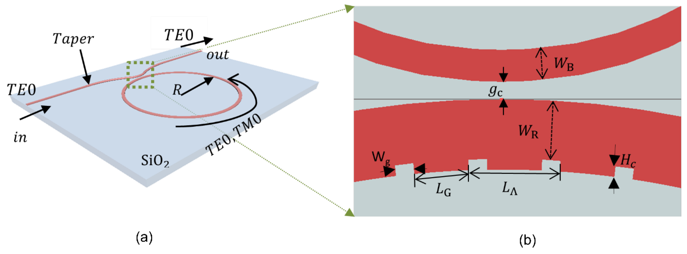
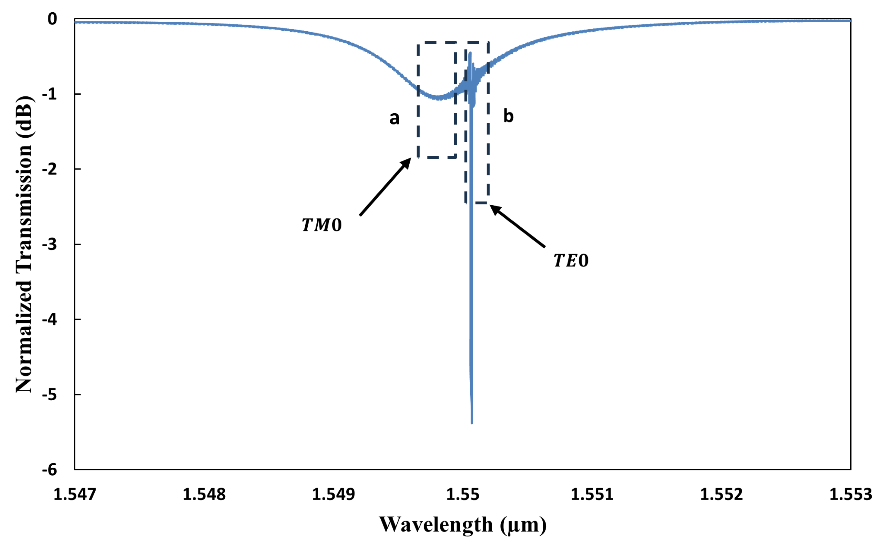
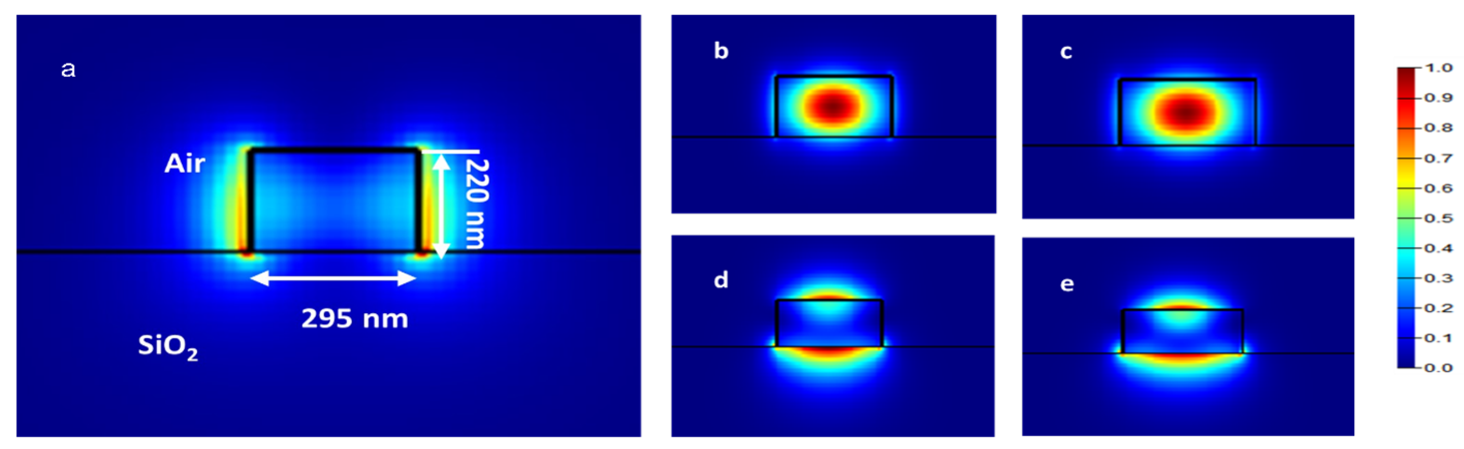
2.1. Structure Design and Working Principle

To construct the optical sensor, an SOI-based photonic platform was utilized, featuring a silicon device layer with a thickness of 220 nm and an insulator layer of 2 µm, topped with air cladding. The refractive indices of the silicon device, insulator layer, and air cladding were 3.48, 1.44, and 1.0, respectively. Figure 1a illustrates a schematic of the proposed structure.
In the design of the optical sensor, the input bus waveguide width was set at 500 nm to facilitate single-mode TE 0 propagation. Near the coupling section, a narrower bus waveguide width W B of approximately 295 nm was employed to enhance coupling efficiency with the ring waveguide. An adiabatic taper section bridges the bus waveguides at the input and the coupling sections. The ring waveguide itself was approximately 550 nm wide, supporting efficient propagation of both TE 0 and TM 0 modes. It features a bend radius of 10 µm, with reference to the circle’s center of the ring waveguide. At the coupling section, the gap between the ring and bus waveguides g c was approximately 0.16 µm. The angular grating dimensions with length L G , height H c , and grating gap W g were 0.568 µm, 0.045 µm, and 0.042 µm, respectively, with a grating period ( L Λ ) of about 0.61 µm, as depicted in Figure 1b. The waveguide sections with widths W R + H c and W R were 595 nm and 550 nm, respectively. The duty cycle D of the grating was selected at approximately 93%. The overall device dimensions were less than 42 μ m × 25 μ m .
The operating principle of the microring resonator is predicated on the simultaneous excitation of the TE 0 and TM 0 modes within the microring cavity. This can be achieved by exciting a continuous-wave broadband light source. The input waveguide, with a thickness of 500 nm, supports only the TE 0 mode, after which the light enters the taper section and couples with the ring waveguide. The width of the ring waveguide was set to 550 nm, enabling the simultaneous support of both TE 0 and TM 0 modes, as shown in Figure 2. Furthermore, it was constructed to accommodate fabrication imperfections. Even with usual deviations during fabrication [23], the mode coupling efficiency was maintained, and both TE 0 and TM 0 modes could be excited and propagated without significant degradation. To mitigate alignment sensitivities, a taper was employed to ensure a gradual transition for stable coupling into the microring waveguide. The taper’s position relative to the ring waveguide was also optimized to facilitate the efficient coupling of both TE 0 and TM 0 modes.
To simplify the phase-matching conditions in the coupling section, a directional coupler-like structure was employed, featuring a zero coupling length and a coupling gap of approximately 0.16 µm. For the optical microring resonator, the resonance condition is described as follows:
m λ res = n eff · L
where m denotes the azimuthal mode number associated with the longitudinal resonances ( m = 1, 2, 3, …), λ res represents the resonating wavelength, and n eff · L signifies the effective optical length of the microring resonator. To achieve this dual mode propagation, the width of the ring waveguide was set at 550 nm when the cladding was air, as shown in Figure 2. This shows that TE 1 modes also propagate in ring waveguides, but they exhibit poor mode confinement within the ring waveguide and tend to diminish over time. Consequently, only the TE 0 and TM 0 modes persisted, as illustrated in Figure 1a.
The coupling strength between the fundamental TE 0 mode of the bus waveguide and that of the ring waveguide was notably higher compared to that between the TE 0 mode of the bus waveguide and TM 0 mode of the ring waveguide. This discrepancy arises because coupling between identical polarization modes is inherently more efficient than between different polarization modes. Figure 3 displays the power coupling ratio of the TE 0 mode in the bus waveguide to both the TE 0 and TM 0 modes supported by the ring waveguide and highlights the distinct extinction ratios attributable to their differing power coupling efficiencies.
For sensing applications, where shifts in the resonance wavelength are critical, the sensing range is governed by the free spectral range (FSR), which corresponds to the spectral spacing between successive longitudinal modes of the ring resonator. However, this range is subject to certain limitations, as shown below:
δ λ res < FSR
where δ λ res indicates the variation in the resonance wavelength. To enhance the measurement range, this shift must be greater than the FSR between the longitudinal modes. To achieve this shift, the incorporation of angular gratings on the inner sidewall of the microring resonator has been proposed. This modification enables selective wavelength operation independent of the FSR and hence facilitates the measurement of target parameters over an expanded range. Our target is to achieve the dominant mode that is able to measure a larger temperature range while measuring RI simultaneously. So, we designed the angular gratings on the inner wall of the microring resonator in such a way that they will facilitate Bragg reflection predominantly for the TE 0 mode and not for the TM 0 mode. Consequently, the device’s response selectively filters out side modes surrounding the dominant mode for TE 0 polarization, leading to a more pronounced resonance for the TE 0 mode relative to the TM 0 mode, as shown in Figure 4. This figure illustrates the simulated normalized power transmission of the dual-polarization angular-grating microring resonator (DP AG-MRR) when the cladding is air. The transmission spectrum is quantified as the ratio of the output-to-input power integrals. The observed variations in the extinction ratios for the TE 0 and TM 0 modes are attributed to their distinct power coupling ratios, as discussed previously. The FSR for the TE 0 mode is extended to approximately 35 nm due to the suppression of side modes. The FSR for the TM 0 mode is approximately 7.6 nm, displaying no dominant mode.
Figure 5 shows dual resonances visible in the output transmission spectrum corresponding to the TE 0 and TM 0 modes. Figure 6a illustrates the normalized electric field profile of the TE 0 mode in the input waveguide, positioned near the coupling region. Additionally, the mode profiles for the TE 0 and TM 0 polarizations, corresponding to the relative widths of the waveguides, are depicted in Figure 6b–e.
The proposed dual-polarization microring resonator with angular gratings (DP AG-MRR) could be fabricated on a 220 nm thick silicon-on-insulator wafer by following a standard fabrication process for silicon photonic devices. The process would begin with spin-coating a 250–300 nm thick electron beam photoresist layer and then defining the microring resonator and waveguide structures using electron beam lithography. This patterned layout is subsequently transferred onto the silicon device layer using inductively coupled plasma reactive ion etching (ICP-RIE), using an C4F8 and SF6 gas mixture [24,25]. Given that manufacturing tolerances can impact the performance of conventional microring resonators [23], careful process calibration would be essential. Lastly, grating couplers could be incorporated at the input/output waveguide facets using an overlay exposure and a shallow etch to facilitate efficient fiber-to-chip coupling [26]. A potential approach for experimentally evaluating the proposed device is to couple light from a tunable laser or a continuous-wave (CW) broadband source, typically operating near 1550 nm, into the chip via polarization-sensitive grating couplers. The chip’s output transmission spectrum can then be recorded using an optical spectrum analyzer [27].

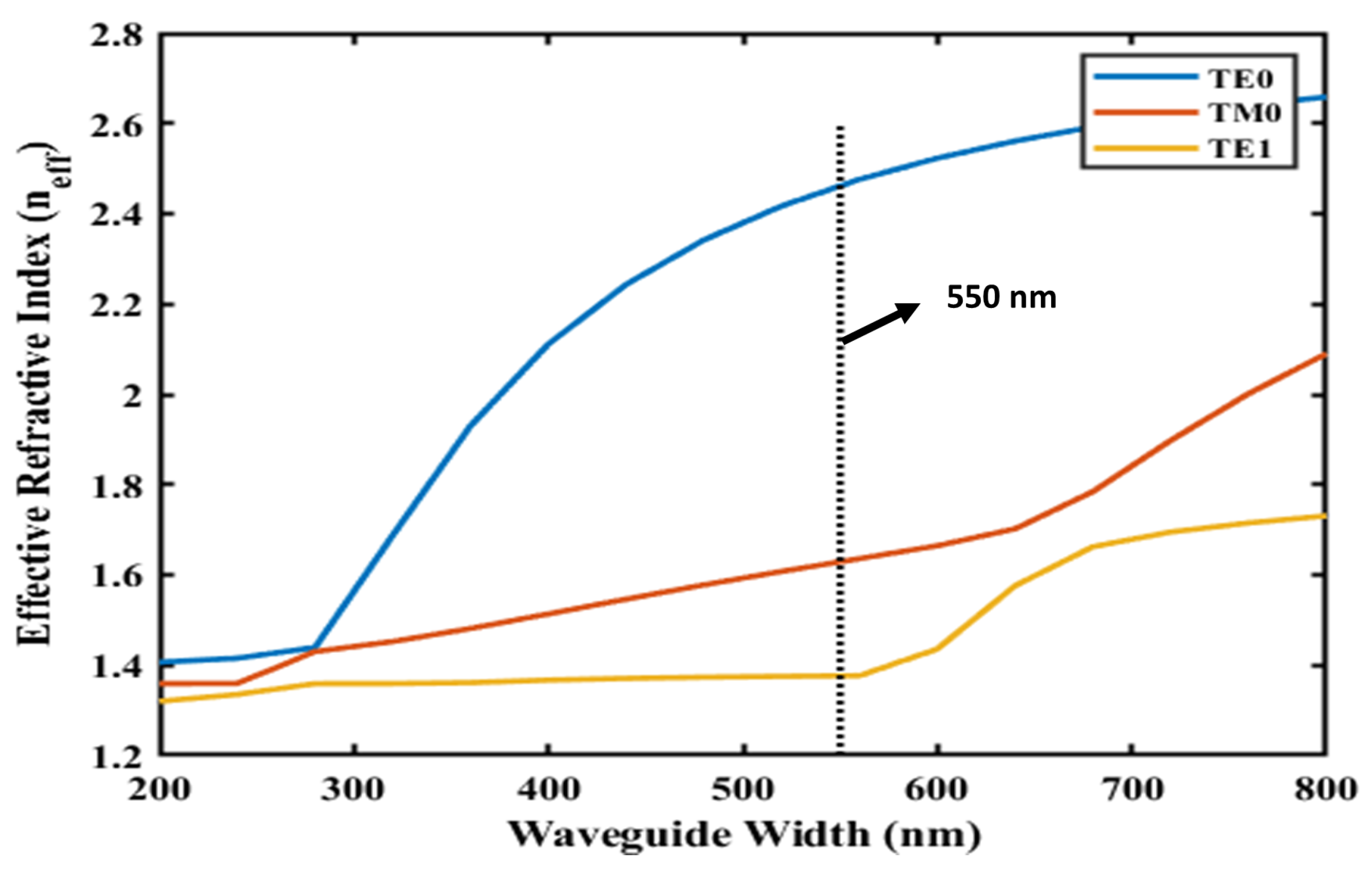
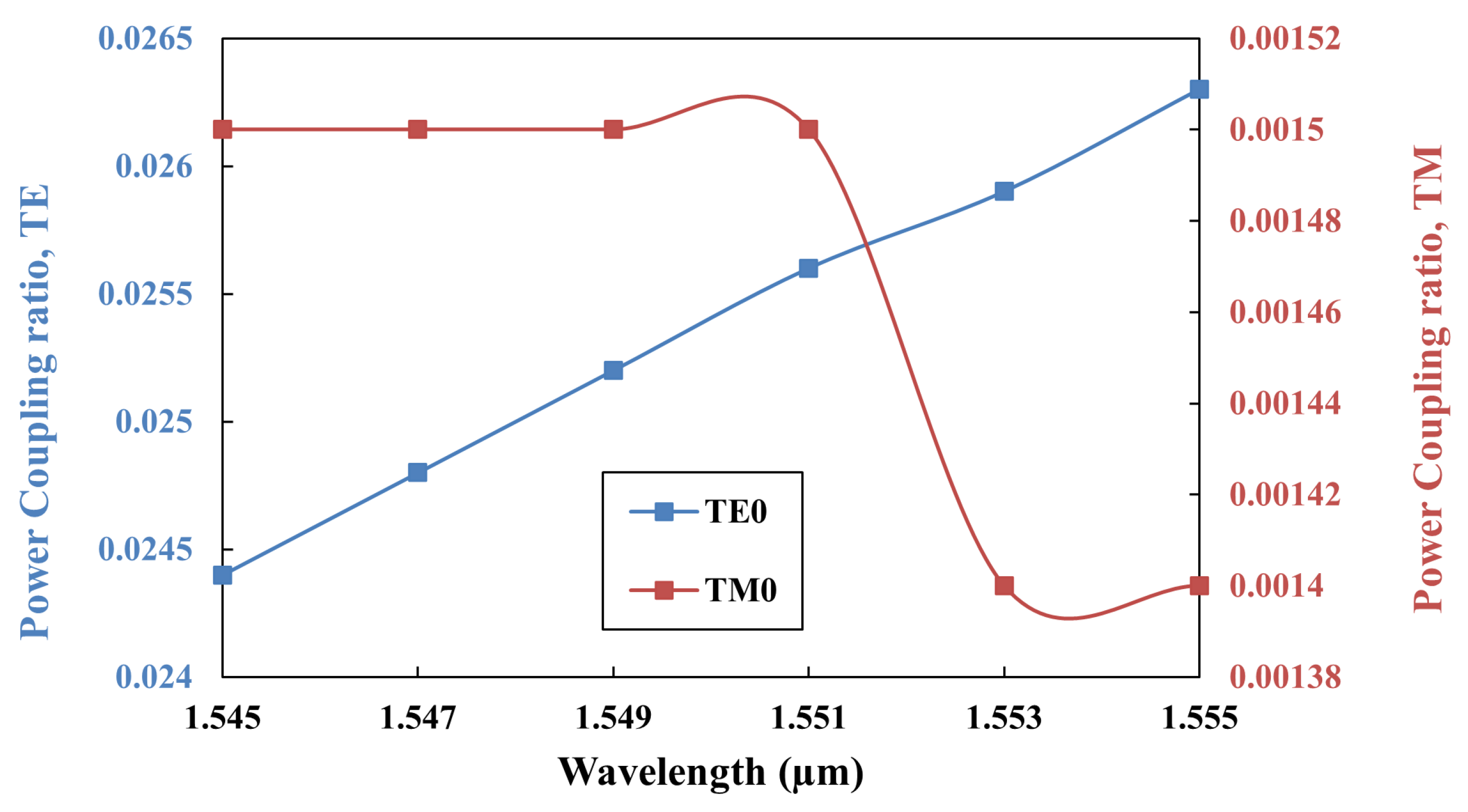
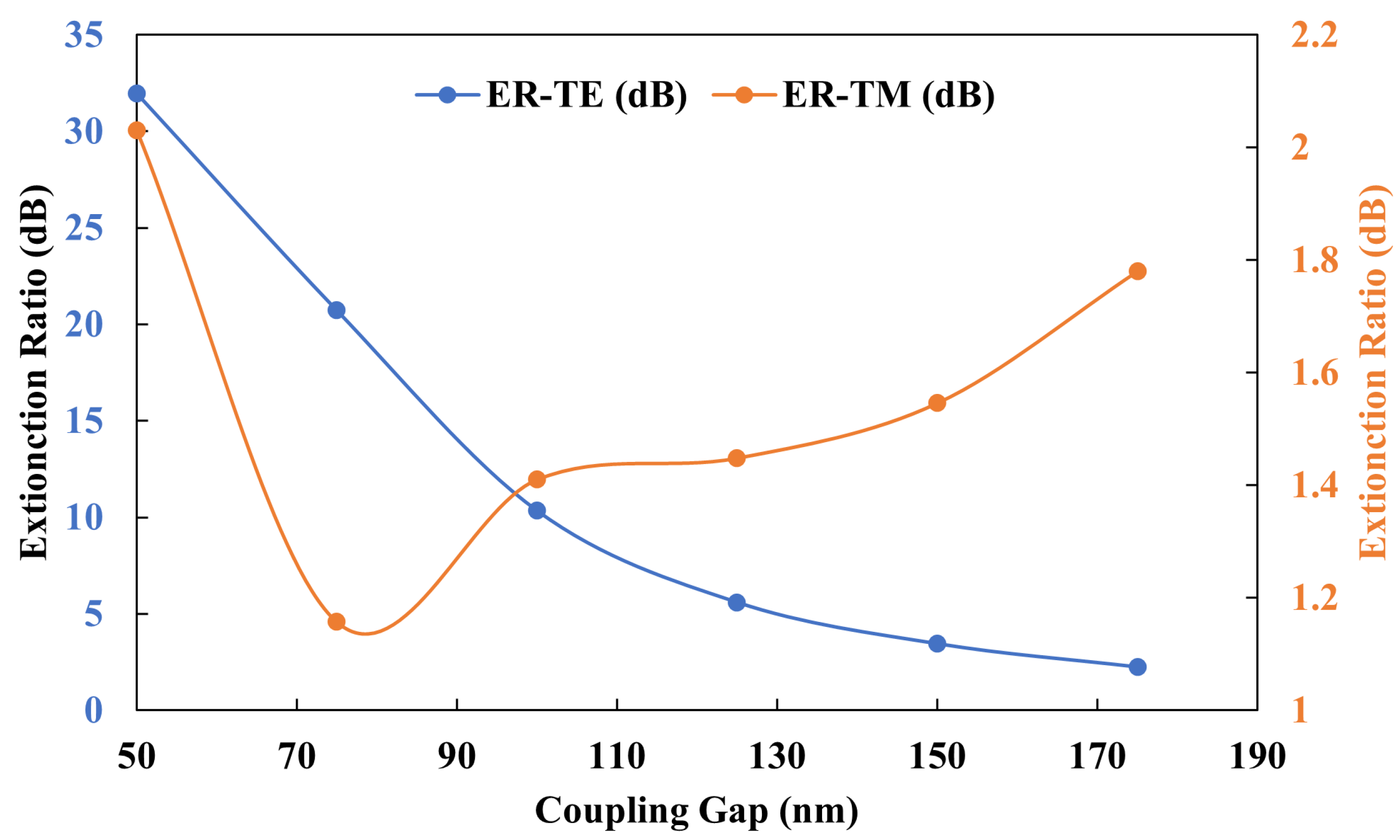
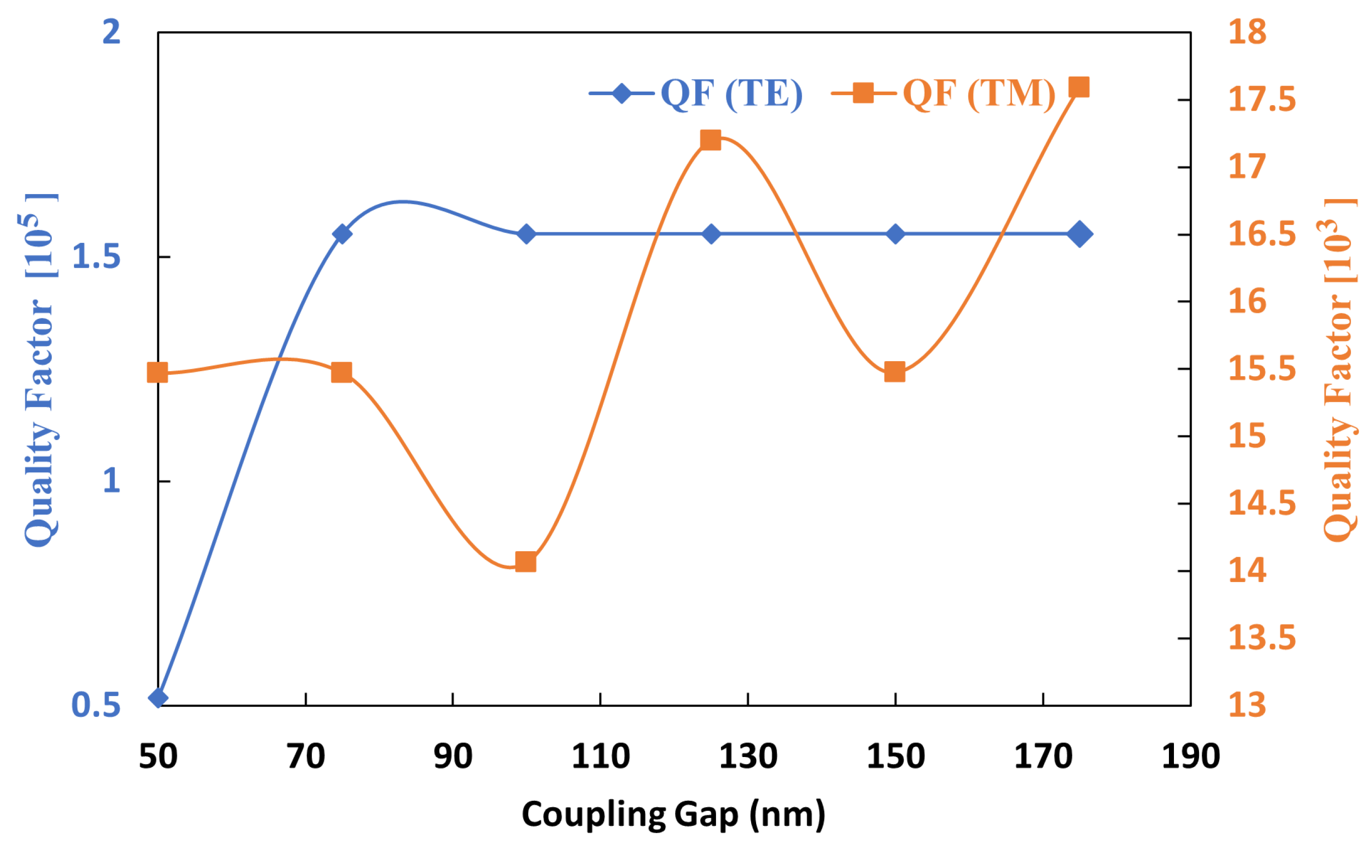
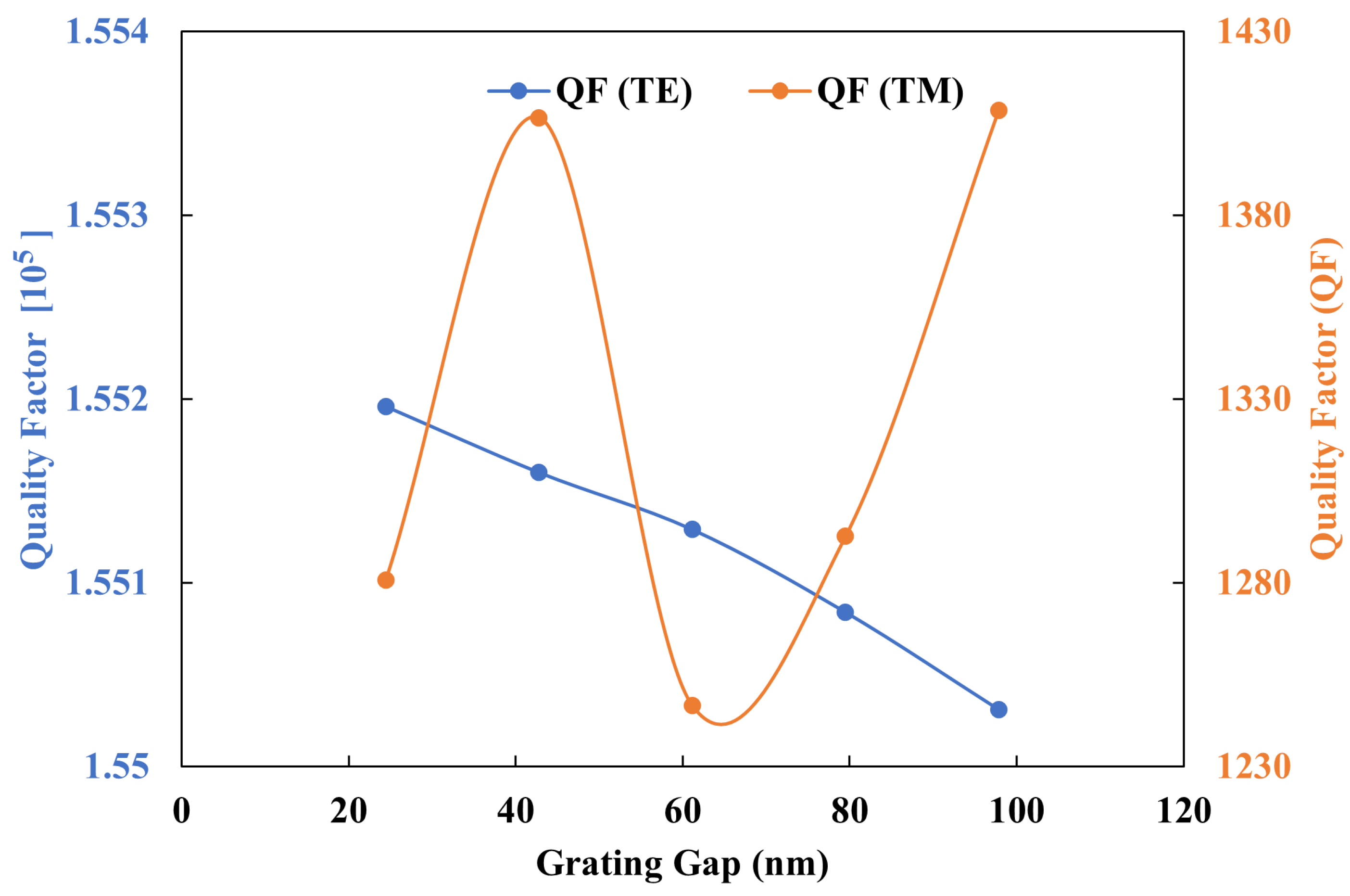
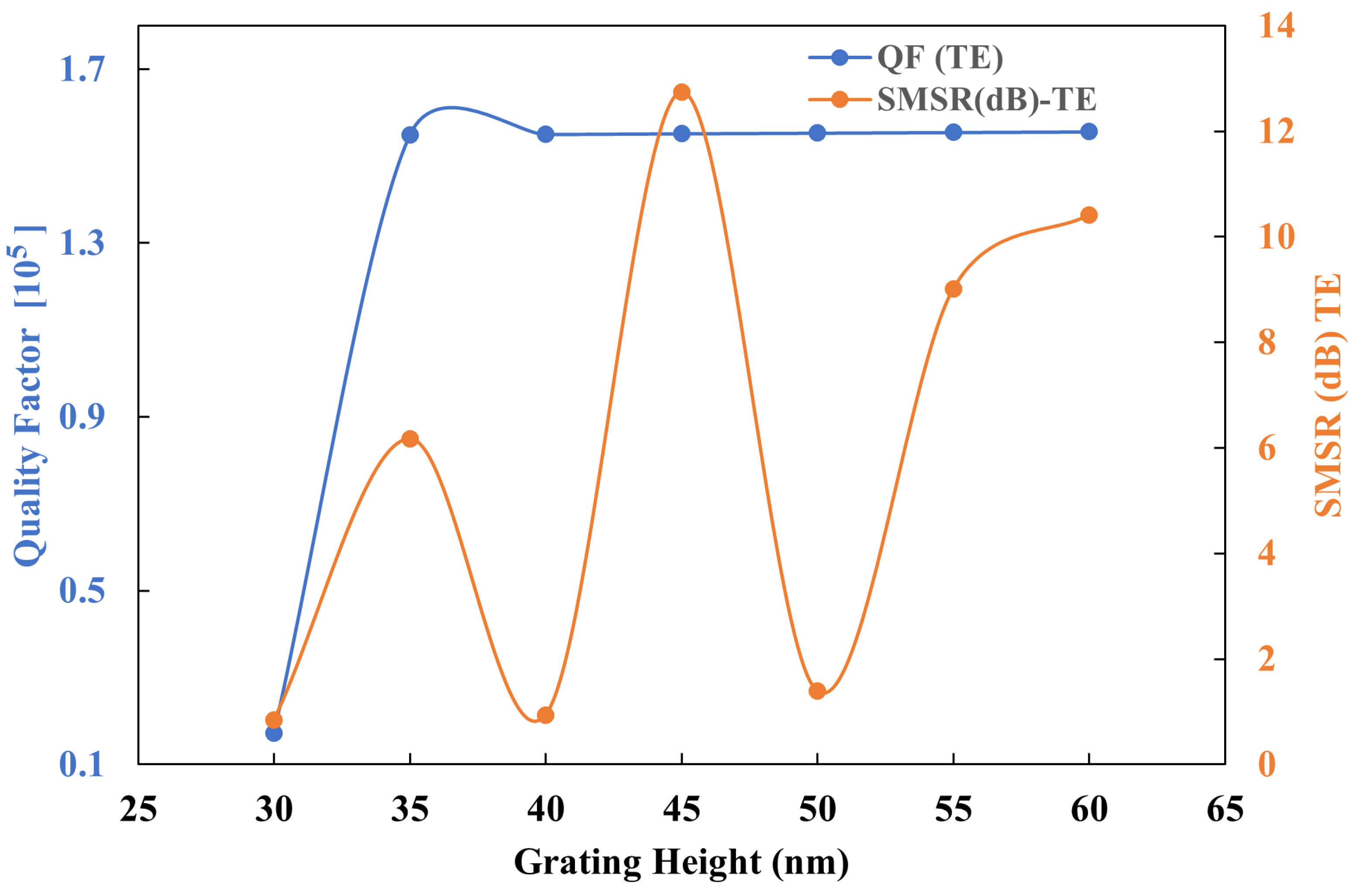
2.2. Parametric Analysis

The device’s performance was optimized through the application of the 2.5-dimensional variational finite-difference time-domain (var-FDTD) approach. For broadband simulations, the variational effective index method was employed. Mesh accuracy was maintained at a value of 4, with a minimum mesh step size of 0.00025 µm selected to effectively balance precision, memory requirements, and simulation duration. The mesh resolution is defined by a minimum step size of 250 pm. In the x, y, and z dimensions, perfectly matched layer (PML) boundaries were employed to absorb incident light with minimal reflection. To further enhance simulation robustness, a stabilized PML profile along the x-axis was implemented, supplemented with additional layers. This configuration utilizes a stretched coordinate PML, improving absorption efficiency and reducing reflection at the boundaries.
The dual-polarization angular-grating microring resonator (DP AG-MRR) was evaluated by injecting light from a fundamental TE-mode source into the input port of the bus waveguide, as described in [28]. Structural parameters, including g c = 160 nm, H c = 40 nm, and D = 93 % , were meticulously optimized. The device demonstrated a pronounced resonant peak for the TE 0 mode at the operational wavelength of 1550 nm, within a spectral range of 1500–1600 nm. The conventional ring resonator featured a free spectral range (FSR) of approximately 9.5 nm, whereas the FSR for the dominant and secondary peaks of the DP AG-MRR was about 35 nm, nearly threefold that of the conventional design for the TE 0 mode.

2.3. Quality Factor, Extinction Ratio, and Side-Mode Suppression

The extinction ratio (ER) and quality factor are critical metrics for assessing the detection capabilities of optical sensors, particularly in terms of sensitivity and detection limits. To attain enhanced sensitivity and minimal detection limits, it is imperative to rigorously evaluate the ER and QF of the proposed sensor. The quality factor is defined as
Q = λ Δ λ
where λ denotes the resonant wavelength, and Δ λ represents the full width at half maximum (FWHM) of the resonance. To achieve a superior quality factor ( Q F ) , it is crucial to minimize losses, which in the DP AG-MRR primarily arise from propagation and coupling. The coupling length is effectively set to zero by opting for a ring-shaped rather than racetrack-shaped resonator, as demonstrated in [29], thereby reducing losses to a minimal extent. The scattering losses due to angular gratings are below 13% [30]. The excess bending losses for a 550 nm wide ring waveguide are less than 0.009 dB/90° [31] for a bend radius of 10 µm, which accounts for mode mismatch losses. A bent waveguide with a width of 295 nm was utilized to optimize coupling, with a coupling gap g c of approximately 160 nm. Other parameters such as the D and H c were also carefully selected at 93% and 40 nm, respectively.
The dependence of the extinction ratio on the coupling gap g c is depicted in Figure 7. Within this figure, it is evident that the ER for the TE 0 mode decreases as g c increases. Conversely, the extinction ratio for the TM 0 mode exhibits a more gradual variation. A g c of 160 nm was strategically selected to facilitate clear differentiation between the extinction ratios of the TE 0 and TM 0 modes.
The relationship between quality factor Q F and coupling gap g c is illustrated in Figure 8. The Q F for the TM 0 mode exhibits minimal variation and remains nearly constant, while Q F for the TE 0 mode shows a rapid increase at lower g c values before stabilizing at higher values. A g c of approximately 160 nm was selected to optimize the Q F , achieving an elevated level of approximately 1.55 × 10 5 , which is particularly advantageous for targeted TE 0 mode temperature sensing.
The duty cycle is a key design parameter in the development of the dual-polarization angular-grating microring resonator (DP AG-MRR). The higher duty cycle generally increases the grating strength, which in turn enhances coupling efficiency and side-mode suppression. However, excessively high duty cycles may result in increased coupling between TE and TM modes, consequently reducing side-mode suppression. Figure 9 illustrates the relationship between the Q F and W g for the transverse electric and transverse magnetic modes. It is observed that an increase in the duty cycle corresponds to an increase in Q F , albeit with a concomitant decrease in the grating gap W g . Given the complexity of fabricating smaller grating heights, a trade-off between Q F and the grating gap is necessary. Consequently, a duty cycle of 93% with a grating height H c of about 45 nm was selected. The duty cycle for the TM 0 mode displays a non-linear relationship and is not the focus of this study. However, it is noteworthy that the maximum Q F for the TM 0 mode occurs at a 93% duty cycle.
The influence of grating height on the Q F and side-mode suppression ratio (SMSR) for the TE 0 mode was evaluated by varying the grating height from 30 nm to 60 nm. As illustrated in Figure 10, the optimal SMSR is achieved at a grating height of 45 nm, which is critical for distinguishing between the TE 0 and TM 0 modes. Notably, the Q F remains relatively constant for the TM 0 mode throughout this range. g c and D are maintained at 160 nm and 93%, respectively.
The effect of fabrication tolerance [23] on the the features of traditional DP AG-MRR is presented in Figure 11 and Figure 12. For the proposed device, the effects associated with the angular grating parameters such as W g , H c , and coupling gap g c are discussed. The optimal device parameters, corresponding to a D of 93%, include a W g of 0.042 µm, H c of 0.045 µm, and g c of 0.16 µm. With these parameters, the Q F is 1.55 × 10 5 , and the E R is 3 dB for the target TE 0 mode. Figure 11 and Figure 12 illustrate the effects of changes in W g , g c , and H c on the deviations Q F and E R from their optimal values. From Figure 11, it is observed that the variation in Q F and E R is less than 20% for the change in W g and g c . The deviation in Q F and E R is consistent for these variations. However, as the tolerance of Δ H c increases, the deviation in Δ Q F also increases, exhibiting opposite behavior for lower tolerance values. The variation in E R from lower to higher tolerance in Δ H c is inconsistent, which can be attributed to the dual-mode overlapping behavior of TE 0 and TM 0 modes. To achieve better results and minimize fabrication tolerance, advanced fabrication technologies with precision on the scale of a few nanometers are required.

3. Results and Discussion

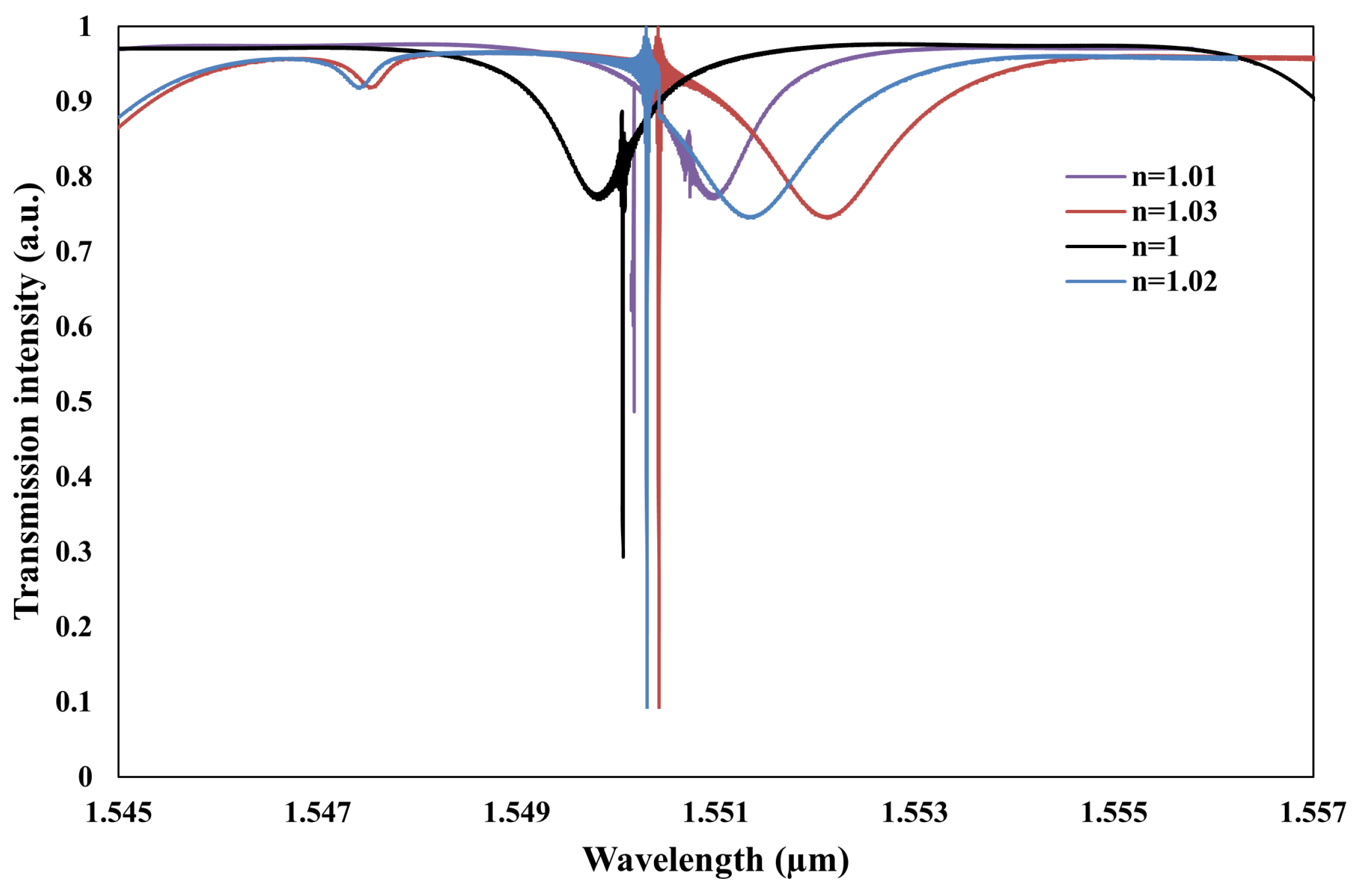
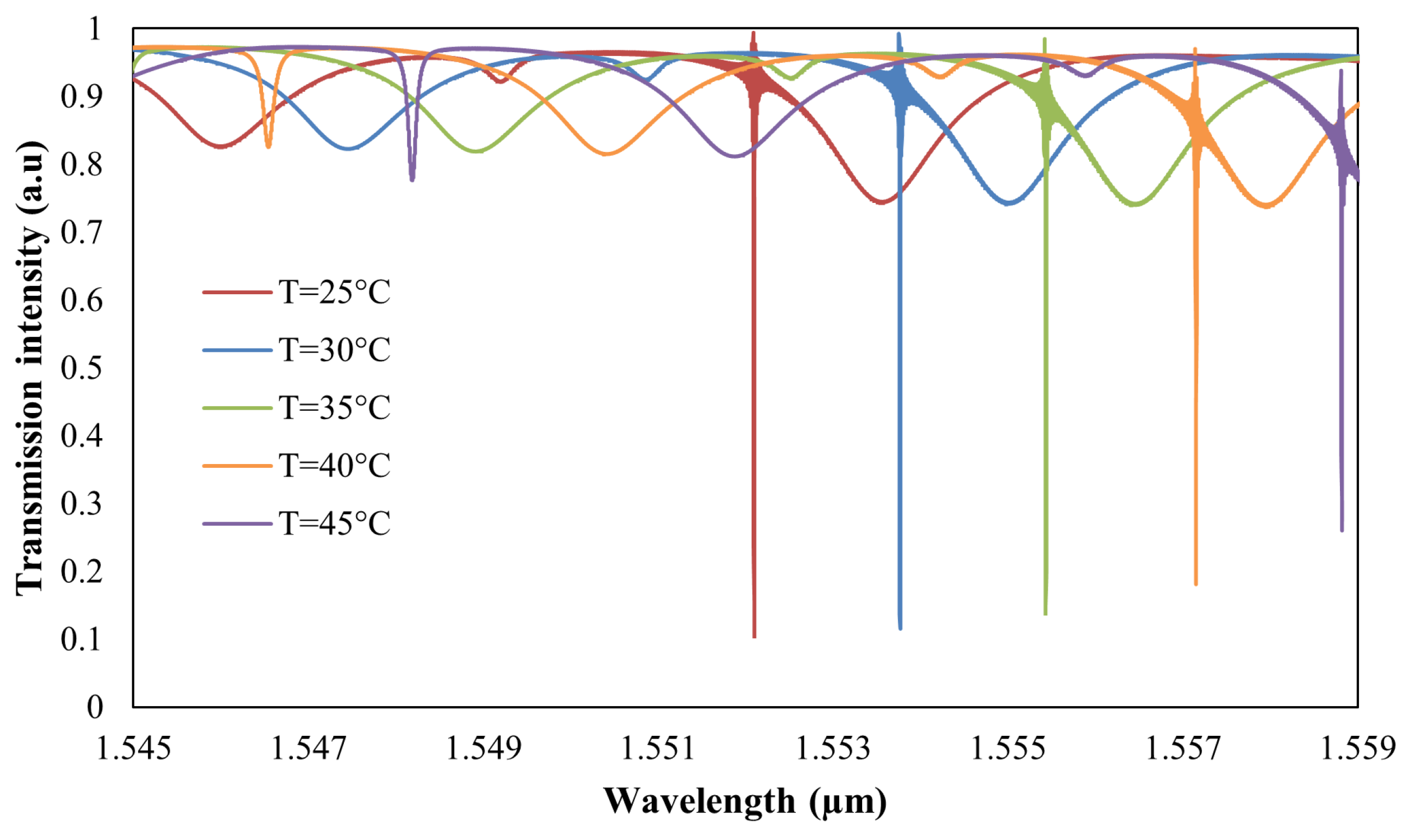
3.1. Resonant Wavelength Shift

Figure 13 presents the simulated transmission spectra for environments of air (n = 1) and chemical gases (n = 1 to 1.03). The analysis indicates a resonance wavelength shift of 2.4 nm for the TM 0 mode, which is limited by the FSR and is not the primary focus of this study. In contrast, a smaller shift of 0.36 nm is observed for the TE 0 mode. Notably, the TM 0 mode exhibits greater light confinement within the cladding region compared to the waveguide region. As depicted in Figure 6, the sensitivities for different polarization types are quantified as S RI , TM 0 = 76.66 nm / RIU and S RI , TE 0 = 13.33 nm / RIU .
Figure 14 presents the variation in the resonance wavelength of the TE 0 mode with respect to temperature, observed with air cladding. The spectral shift of the resonance wavelength corresponding to the TE 0 is recorded at 1.67 nm, which is greater than the 1.30 nm shift observed for the TM 0 mode. This variation is due to the significantly higher thermo-optic coefficient of silicon 1.8 × 10 4 × K 1  [17], in contrast to that of air cladding 9.8 × 10 7 × K 1  [32]. Consequently, the temperature sensitivity of the TE 0 mode, quantified at S T , TE 0 = 334 pm / ° C exceeds that of the TM 0 mode, which is measured at S T , TM 0 = 260 pm / ° C . Furthermore, the sensitivity ratios for the RI, S RI , TM 0 S RI , TE 0 = 5.75 and temperature S T , TM 0 S T , TE 0 = 0.78 differ significantly, facilitating the simultaneous detection of both parameters. Notably, the RI sensitivity is relatively low, indicating that the dual-resonance approach is well-suited for applications where temperature measurement is of primary importance. To enhance RI sensitivity while maintaining temperature sensing capabilities, a viable approach is to incorporate a dual-polarization, subwavelength-based structure. This method will be explored and presented in our future work.

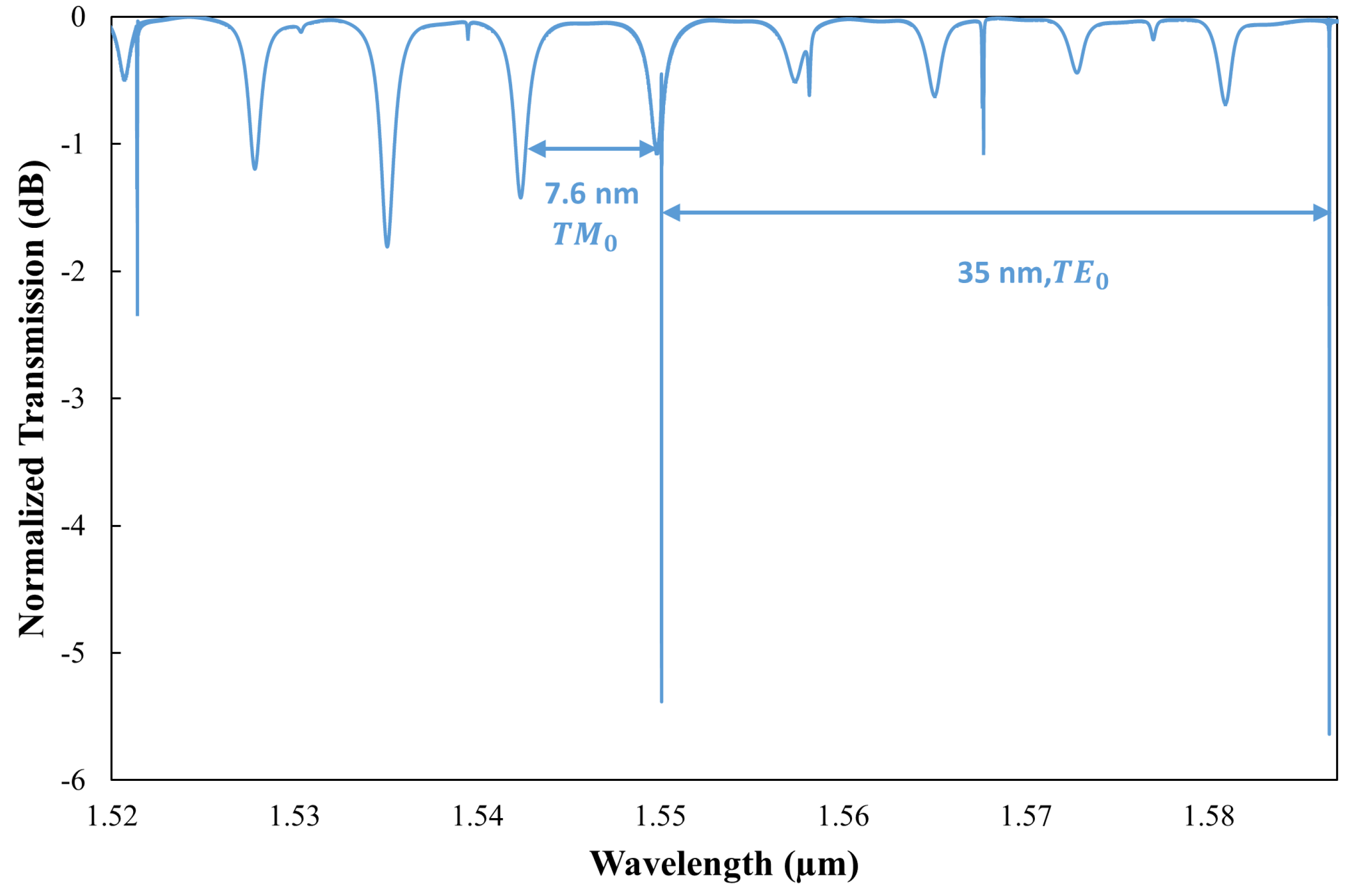
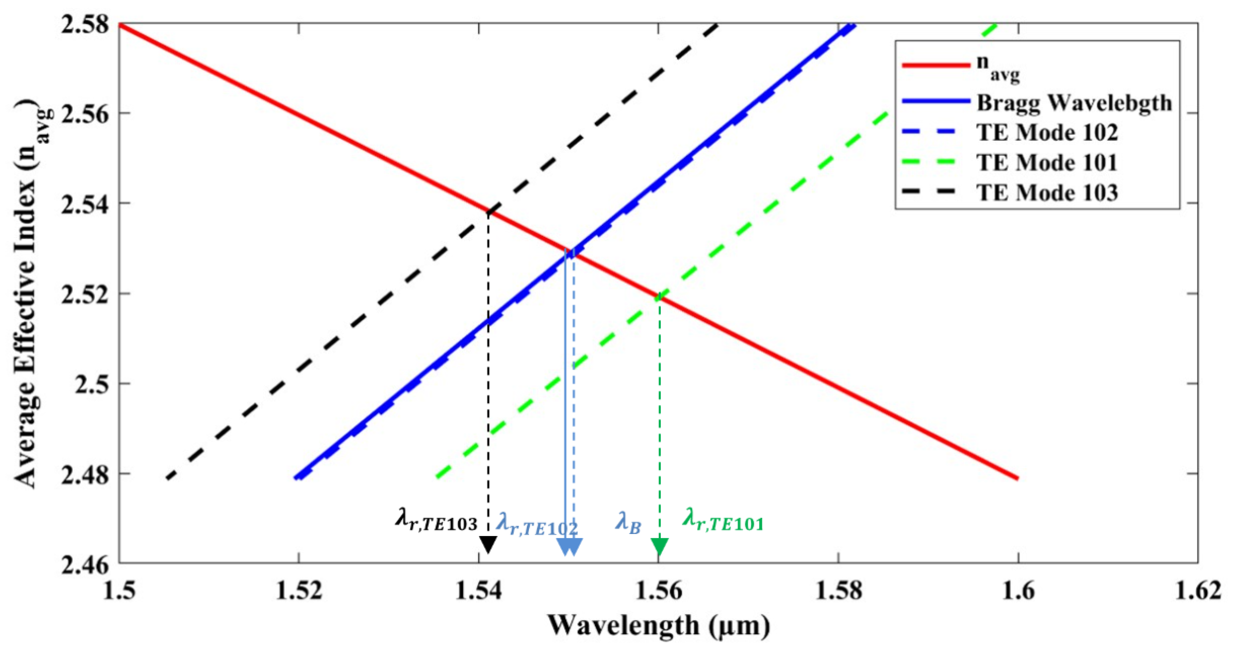
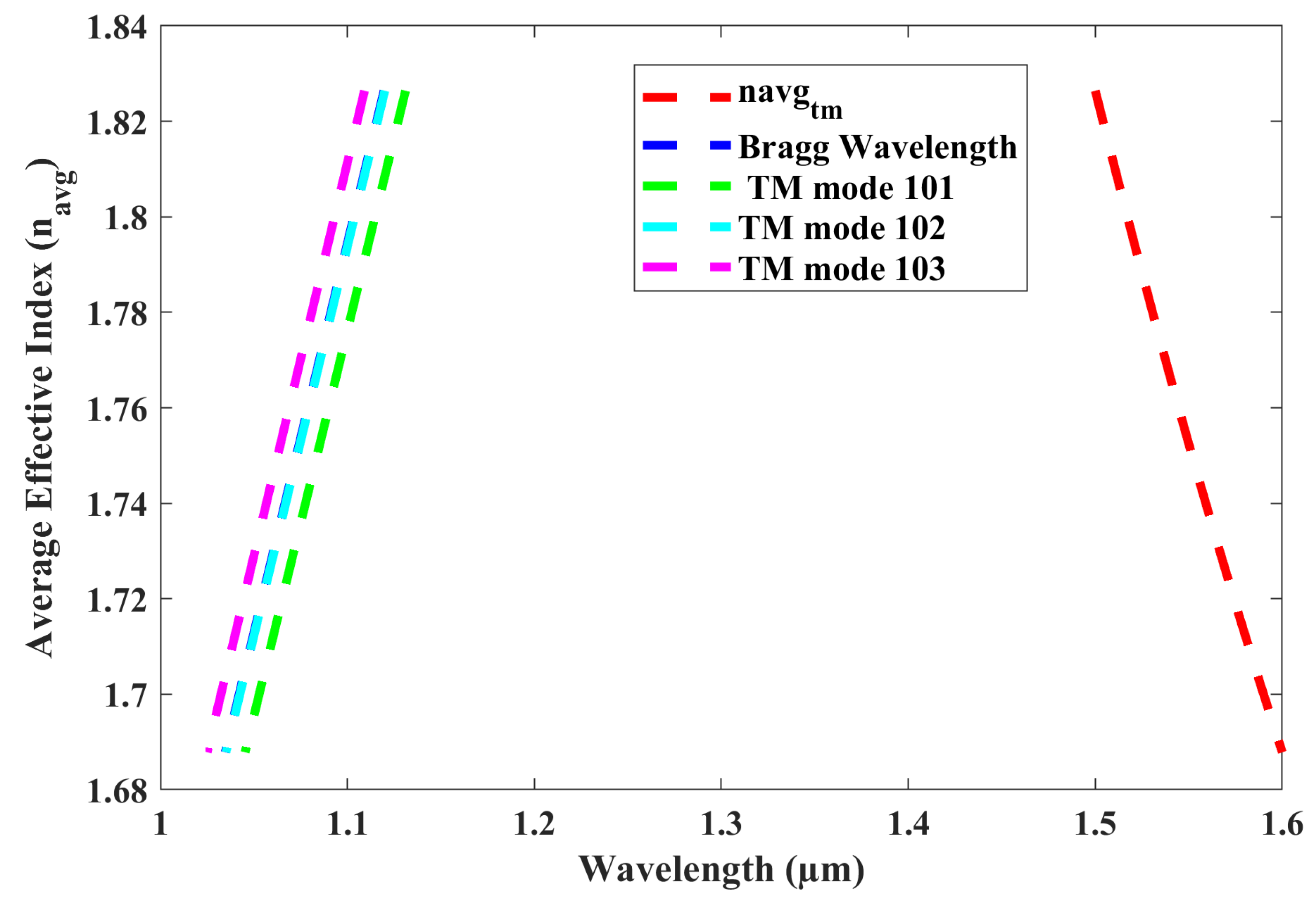
3.2. Wavelength Selection

Wavelength selectivity for the fundamental TE 0 mode was investigated using eigensolver analysis [33]. This analysis was applied to waveguide sections with widths W R + H c and W R , with widths of 595 nm and 550 nm, respectively, as depicted in Figure 1b. To demonstrate wavelength selectivity, Figure 15 features a solid red line representing the equivalent wavelength of the dual-polarization angular-grating microring resonator (DP AG-MRR), calculated using Rytov’s formula [34], as below:
n avg 2 = D · n eff 1 2 + ( 1 D ) · n eff 2 2
Here, n eff 1 and n eff 2 represent the effective refractive indices of the waveguide segments with widths W R + H c and W R , respectively. The solid blue line in the diagram represents the Bragg wavelength, intersecting the red line at 1550 nm. The dashed black, blue, and green lines correspond to mode numbers 103, 102, and 101, respectively. The wavelengths for modes 101 and 103 are significantly divergent from the Bragg wavelengths; therefore, only the mode proximate to the Bragg wavelength, specifically mode number 102 (dashed blue line), will be selected as the dominant mode. The wavelength selectivity of the TM 0 mode will be explored in our forthcoming research, which will include investigations into the dual-polarization angular-grating microring resonator (DP-AG MRR). Figure 16 demonstrates that angular gratings have no impact on the TM 0 mode, resulting in no wavelength selection from the TM 0 mode. The dashed red line represents the average effective index of the waveguide, which corresponds to the same wavelength range as the TE 0 mode, as both modes propagate within the same ring waveguide. The dashed blue line in Figure 16 indicates the Bragg wavelength within the 1.03 to 1.12 µm range, which is significantly different from the 1.5 to 1.6 µm wavelength range. Although mode 102 is close to the Bragg wavelength for the TM 0 mode, it is not selected because it does not intersect with the dashed red line representing the average effective index of the waveguide. This behavior is evident in the transmission spectrum shown in Figure 4. Notably, this study marks the first successful demonstration of a dominant TE 0 mode using angular gratings within a dual-polarization microring resonator. Table 1 provides a comparative analysis of the current study on the simultaneous detection of RI and temperature through MRR-based optical sensing.

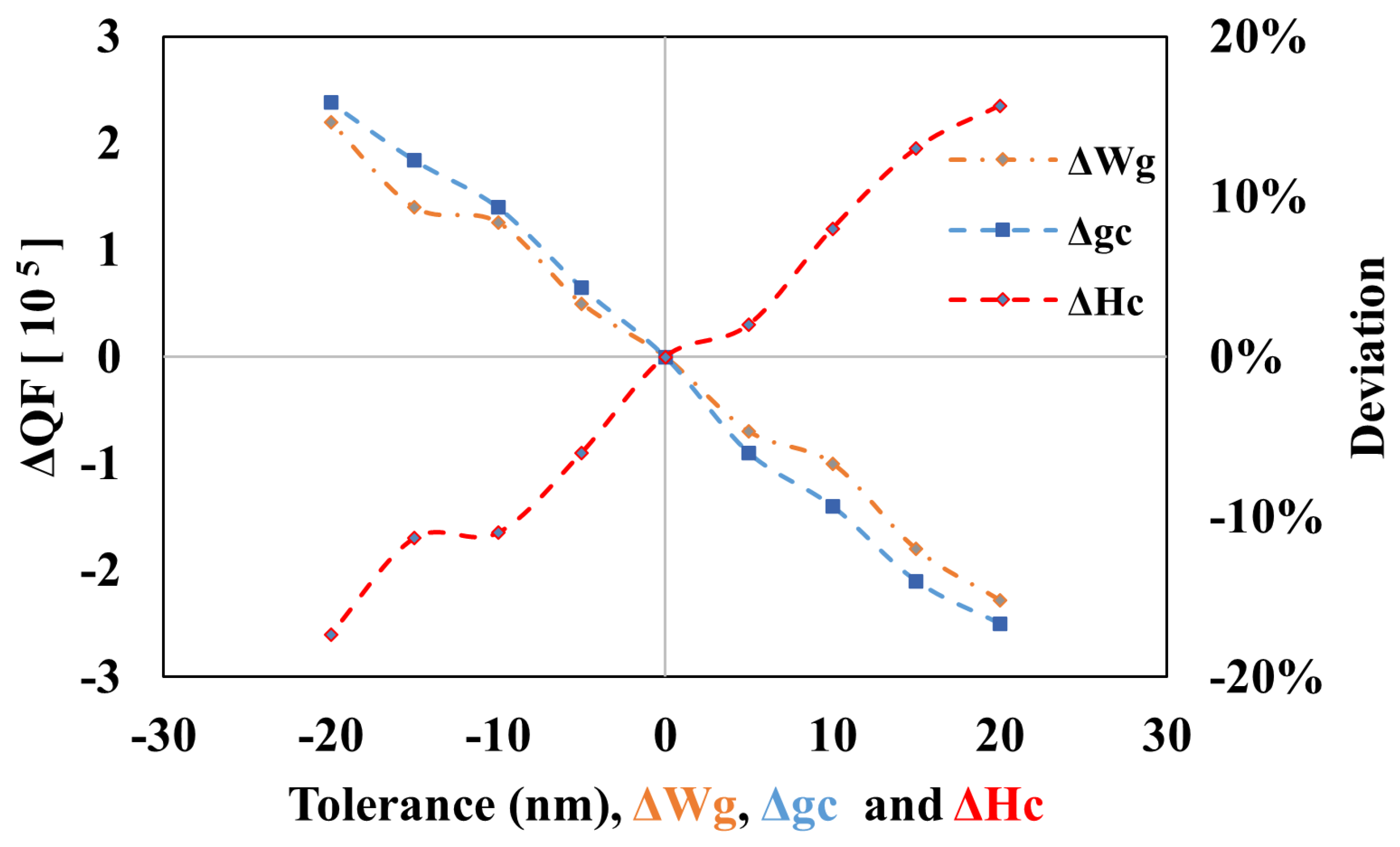
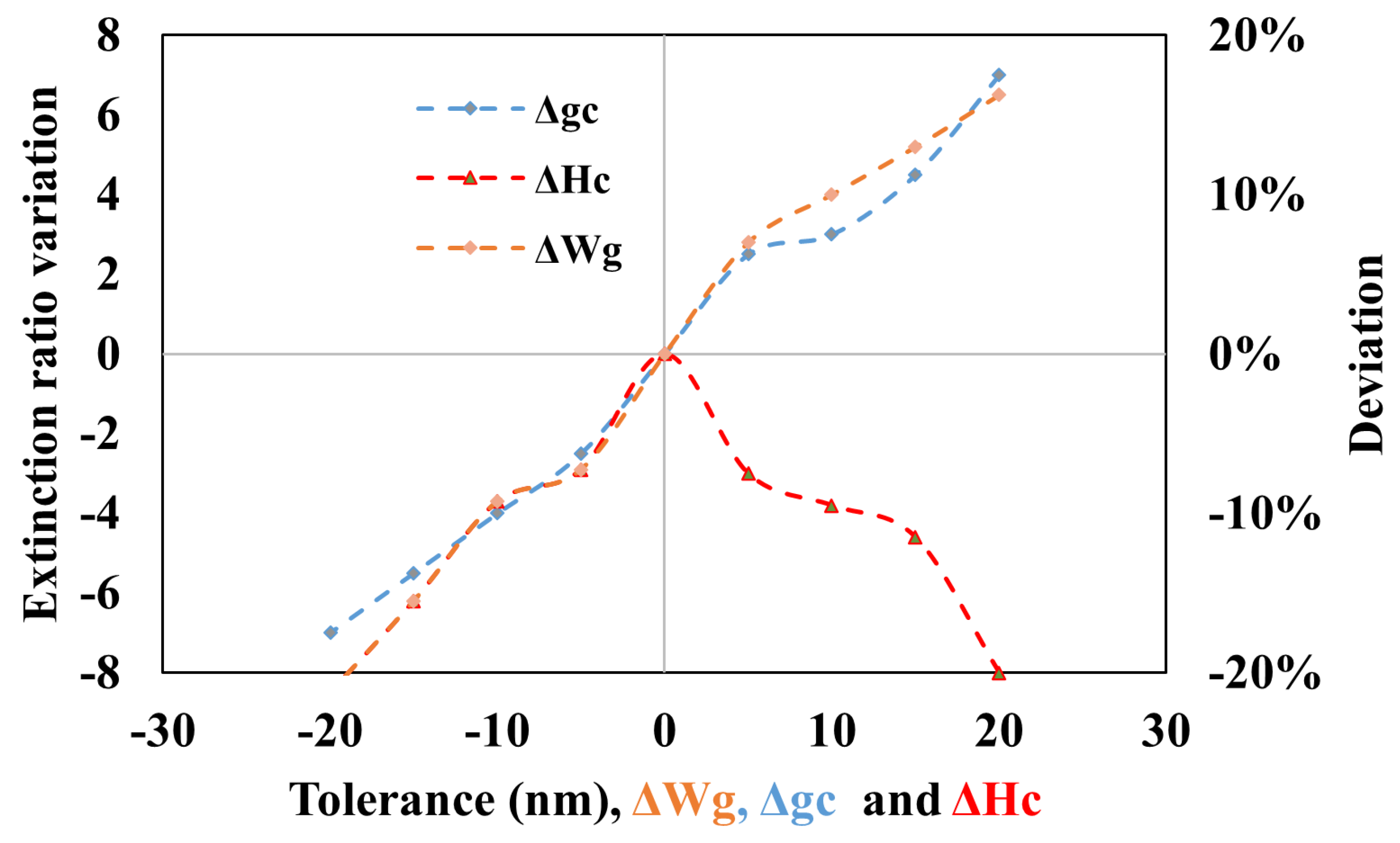
3.3. Sensing Analysis

The sensing characteristics of DP AG-MRR are quantified using the sensitivity matrix SM T , n defined below:
SM T , RI = S T , TE 0 S RI , TE 0 S T , TM 0 S RI , TM 0
where S T , TM 0 and S R I , TM 0 denote the sensitivities to temperature and RI, respectively, under TM 0 polarization, while S T , TE 0 and S R I , TE 0 represent the corresponding sensitivities under TE 0 polarization. The variations in RI and temperature can be determined using the following equations:
Δ T Δ n = SM T , RI 1 · Δ λ TE 0 Δ λ TM 0
Δ T = S RI , TM 0 · Δ λ TE 0 S RI , TE 0 · Δ λ TM 0 det ( SM T , RI )
Δ n = S T , TE 0 · Δ λ TM 0 S T , TM 0 · Δ λ TE 0 det ( SM T , RI )
From Equations (7) and (8), it is clear that changes in temperature and RI are calculated using the combined effect of wavelength deviation represented as Δ λ TE 0 and Δ λ TM 0 due to TE 0 and TM 0 polarizations, respectively, which ensures accurate measurement.
The sensitivity of SOI-based MRR is attributed to the corresponding deviation in the effective refractive index, which is induced by variations in the surrounding temperature and RI. This relationship was previously established in [38].
Sensitivity var , p = δ λ p δ var = δ n eff , p δ var × δ λ p δ n eff , p
where δ var represents the change in the variable, either RI or temperature; p denotes the polarization, either TM 0 or TE 0 ; λ p denotes the resonance wavelength corresponding to polarization state p; and δ n eff , p indicates the change in the effective refractive index for polarization p.
The ambient variations change the n eff , and this can be described by
δ n eff , p δ var ( λ ) = A clad , p ( λ ) · δ n clad δ var ( λ ) + A c , p ( λ ) · δ n c δ var ( λ ) + A buff , p ( λ ) · δ n buff δ var ( λ )
Here, A clad , p , A c , p , and A buff , p represent the confinement factors in the cladding, core, and buffer regions, respectively, for polarization p, as illustrated in Figure 12. If the ambient RI changes, no change is induced in ( n eff ) for the core and buffer layers, as δ n c δ n ( λ ) = 0 and δ n buff δ n ( λ ) = 0 , respectively. Regarding the effect of temperature changes on the cladding, silicon, and silica layers, it is essential to consider the thermo-optic coefficients of these materials. Given that the thermo-optic coefficients [39,40] for liquid solvents and silicon layers are significantly higher than those for silica, the impact of the silica layer on temperature variation can be disregarded. Consequently, using Equation (6), we derive the following equations:
S e n s i t i v i t y n , p = A clad , p ( λ ) · δ n clad δ n ( λ ) · δ λ p δ n eff , p
S e n s i t i v i t y T , p = A clad , p ( λ ) · δ n clad δ T ( λ ) + A c , p ( λ ) · δ n c δ T ( λ ) δ λ p δ n eff , p
For the equations presented, S e n s i t i v i t y n , T M 0 will be greater than S e n s i t i v i t y n , T E 0 . This discrepancy arises because S e n s i t i v i t y n , p is strongly influenced by the confinement factor within the cladding region, and the TM 0 polarization exhibits greater field intensity within this region. Considering the substantially lower thermo-optic coefficient of air compared to that of silicon [32,41], S e n s i t i v i t y T , T E 0 is correspondingly lower in air than in the silicon layer. Additionally, S e n s i t i v i t y T , T M 0 remains low in silicon due to the predominance of TE 0 fields within the silicon core, as opposed to TM 0 fields, which are more concentrated in the cladding region.
Consequently, the sensitivities to both RI and temperature vary between TE 0 and TM 0 polarizations. The incorporation of angular gratings facilitates the simultaneous measurement of the RI and temperature, enabling a broader range of temperature assessment. Utilizing Equations (5) and (6) and incorporating sensitivity values corresponding to specific polarizations, we formulate the following equation:
Δ T Δ n = 13.33 nm / RIU 334 pm / C 76.66 nm / RIU 260 pm / C 1 Δ λ TE 0 Δ λ TM 0
One key parameter for assessing sensor performance is the limit of detection (LOD). In this work, we primarily focus on extending the FSR for temperature measurement while achieving an improved LOD, simultaneously monitoring both the RI and temperature. Using the expression presented in [42], our structure achieves an LOD of approximately 2.99 × 10 5 for the TE 0 mode, which is employed for temperature sensing, while the LOD for the TM 0 mode is 1.14 × 10 2 :
LOD = λ res Q S
As shown in Table 1, our structure exhibits a superior LOD and sensitivity for temperature variations, making it particularly suitable for applications where ambient temperature changes are of prime importance.
To assess the viability of simultaneous measurements with our device, we first set the temperature T set to 27 °C and the refractive index RI set ) to 1 (the refractive index of air) in the simulation setup. The corresponding resonant wavelengths, λ T , set and λ RI , set , were measured to be 1550.07 nm and 1549.81 nm, respectively. Using Equation (13), we then varied the values of temperature and refractive index (RI) and calculated Δ λ TE 0 and Δ λ TM 0 for each variation group with respect to the set conditions. Table 2 presents the measured values of Δ λ TE 0 and Δ λ TM 0 for six distinct groups, enabling the determination of changes in temperature ( Δ T ) and RI ( Δ n ).

4. Conclusions

In this study, we introduced a dual-polarization angular-grating microring resonator (DP AG-MRR)-based structure incorporating angular gratings and a directional coupler-like coupling section, designed to extend the measurement range for temperature variations. For the first time, we explored the capability of the angular-grating MRR (AG-MRR) to simultaneously detect changes in temperature and RI across dual polarization modes within its transmission spectra, thereby achieving a comprehensive measurement range for ambient temperature variations. Through parameter optimization, we established a set of resonance pairs with distinct sensing ratios for temperature and RI. The simulated RI sensitivities of 13.33 nm/RIU and 76.66 nm/RIU, along with temperature sensitivities of 334 pm/°C and 260 pm/°C, were obtained by analyzing the resonance shift in the modes in response to RI variations at different temperatures. The simulations yielded an FSR of about 35 nm with a detection limit as low as 2.99 × 10 5 , significantly enhancing the measurement range for temperature while concurrently sensing the ambient RI. Furthermore, we assessed the impact of dimensional deviations in the angular gratings and coupling region parameters, such as the coupling gap g c , grating gap W g , and duty cycle (D), on the performance of the DP AG-MRR. Given its straightforward configuration and compatibility with various silicon-on-insulator (SOI) devices, this design proves advantageous for applications requiring simultaneous detection with a single measurement including a larger temperature range.

Author Contributions

Conceptualization, M.F.Q.; methodology, M.F.Q.; software, M.Z.; validation, S.S.; formal analysis, S.S.; investigation, M.F.Q. and A.S.R.; resources, M.M.A.; data curation, M.F.Q.; writing—original draft preparation, M.F.Q. and A.S.R.; writing—review and editing, M.Z., W.B. and S.S.; visualization, S.S. and M.M.A.; supervision, M.Z. and S.S.; project administration, M.F.Q.; funding acquisition, S.S. and W.B. All authors have read and agreed to the published version of the manuscript.

Funding

Open Access Funding by the Graz University of Technology, Austria.

Data Availability Statement

All original findings presented in this study are contained within the article.

Conflicts of Interest

The authors declare no conflicts of interest.

Abbreviations

The following abbreviations are used in this manuscript:
SOISilicon-On-Insulator;
TETransverse Electric;
TMTransverse Magnetic;
RIRefractive Index;
SPRSurface Plasmon Resonance;
MRRMicroring Resonator;
FSRFree Spectral Range;
MCRWMetal-Clad Ridge Waveguide;
DP AG-MRRDual-Polarization Angular-Grating microring resonator;
ICP-RIEInductively Coupled Plasma Reactive Ion Etching;
CWContinuous Wave;
PMLPerfectly Matched Layer;
ERExtinction Ratio;
QFQuality Factor;
LODLimit of Detection.

References

  1. Alonso-Murias, M.d.C.; Velázquez-González, J.S.; Monzón-Hernández, D. SPR Fiber Tip Sensor for the Simultaneous Measurement of Refractive Index, Temperature, and Level of a Liquid. J. Light. Technol. 2019, 37, 4808–4814. [Google Scholar] [CrossRef]
  2. Liu, M.; Leng, X.; Ni, W.; Shum, P. Simultaneous and Ultrasensitive Measurement of Refractive Index and Temperature Based on SPR of Hollow-Core Anti-resonant Fibers. Plasmonics 2024, 19, 3091–3100. [Google Scholar] [CrossRef]
  3. Zhang, Y.; Liu, M.; Zhang, Y.; Liu, Z.; Yang, X.; Zhang, J.; Yang, J.; Yuan, L. Simultaneous measurement of temperature and refractive index based on a hybrid surface plasmon resonance multimode interference fiber sensor. Appl. Opt. 2020, 59, 1225–1229. [Google Scholar] [CrossRef]
  4. Yu, F.; Xue, P.; Zhao, X.; Zheng, J. Simultaneous Measurement of Refractive Index and Temperature Based on a Peanut-Shape Structure In-Line Fiber Mach–Zehnder Interferometer. IEEE Sens. J. 2019, 19, 950–955. [Google Scholar] [CrossRef]
  5. Freitas, A.I.; Pereira, D.; Bierlich, J.; Marques, J.C.; Ferreira, M.S. Simultaneous measurement of refractive index and temperature using a balloon-type optical fiber sensor. Optik 2024, 309, 0030–4026. [Google Scholar] [CrossRef]
  6. Butt, M.A. Plasmonic Sensor System Embedded with Orthogonal Mode Couplers for Simultaneous Monitoring of Temperature and Refractive Index. Plasmonics 2025, 20, 459–469. [Google Scholar] [CrossRef]
  7. Geetha, T.S.; Chellaswamy, C.; Kaliraja, T. Optimized convolutional neural network-based temperature and refractive index fiber optic sensor. J. Opt. 2024. [Google Scholar] [CrossRef]
  8. Gou, Z.; Wang, C.; Han, Z.; Nie, T.; Tian, H. Artificial neural networks assisting the design of a dual-mode photonic crystal nanobeam cavity for simultaneous sensing of the refractive index and temperature. Appl. Opt. 2022, 61, 4802–4808. [Google Scholar] [CrossRef]
  9. Dhara, P.; Singh, V.K.; Kumar, A.; Olivero, M.; Perrone, G. Reflection based silicon incorporated silver coated fiber optic SPR sensor for refractive index and temperature measurement. Microsyst. Technol. 2024, 30, 913–922. [Google Scholar] [CrossRef]
  10. Duan, C.; Li, J.; Zhang, K.; Tian, M. Optical fiber dual-parameter sensors based on different kinds of interferometers for measuring refractive index and temperature: A review. Opt. Quant. Electron. 2024, 56, 262. [Google Scholar] [CrossRef]
  11. Yu, X.; Zuo, S.; Zhang, Y.; Ma, Y.; Wang, R.; Yang, W.; Tian, K.; Geng, T.; Wang, P. Mach–Zehnder interferometer based on peanut structure for temperature and refractive index measurement. Opt. Quant. Electron. 2024, 56, 492–497. [Google Scholar] [CrossRef]
  12. Liu, Q.; Wang, D.; Li, X.; Gao, H.; Yu, D. Simultaneous measurement of temperature and liquid refractive index based on fiber open Fabry-Pérot cavity and Bragg grating. Optoelectron. Lett. 2024, 20, 477–482. [Google Scholar] [CrossRef]
  13. André, R.M.; Warren-Smith, S.C.; Becker, M.; Dellith, J.; Rothhardt, M.; Zibaii, M.I.; Latifi, H.; Marques, M.B.; Bartelt, H.; Fraz, O. Simultaneous measurement of temperature and refractive index using focused ion beam milled Fabry-Perot cavities in optical fiber micro-tips. Opt. Express 2016, 24, 14053–14065. [Google Scholar] [CrossRef]
  14. Zhu, Y.; Zhang, Y.; Tang, Q.; Li, S.; Zheng, H.; Liang, D.; Xiao, H.; Du, C.; Yu, Y.; Ruan, S. Double-Cavity Fabry–Perot Interferometer Sensor Based on Polymer-Filled Hollow Core Fiber for Simultaneous Measurement of Temperature and Gas Pressure. Sensors 2025, 25, 2396. [Google Scholar] [CrossRef] [PubMed]
  15. Lu, X.; Yu, X.; Zhou, J.; Chang, M.; Lu, D. An Ultra-Wide Range D-Shaped Fiber SPR Sensor with a Nanostructure of Gold–MoS2 and Sodium for the Simultaneous Measurement of Refractive Index and Temperature. Sensors 2025, 25, 377. [Google Scholar] [CrossRef] [PubMed]
  16. Yang, S.; Wu, Y.; Yang, Y.; Wang, C.; Tian, H. High sensitivity and anti-external interference dual-parameter sensor based on a multimode slotted photonic crystal nanobeam cavity. J. Mod. Opt. 2021, 68, 357–364. [Google Scholar] [CrossRef]
  17. Liu, P.; Shi, Y. Simultaneous measurement of refractive index and temperature using cascaded side-coupled photonic crystal nanobeam cavities. Opt. Express 2017, 25, 28398–28406. [Google Scholar] [CrossRef]
  18. Claes, T.; Molera, J.G.; Vos, K.D.; Schacht, E.; Baets, R.; Bienstman, P. Label-Free Biosensing With a Slot-Waveguide-Based Ring Resonator in Silicon on Insulator. IEEE Photonics J. 2009, 1, 197–204. [Google Scholar] [CrossRef]
  19. Ma, T.; Sun, L.; Yuan, J.; Sang, X.; Yan, B.; Wang, K.; Yu, C. Integrated label-free optical biochemical sensor with a large measurement range based on an angular grating-microring resonator. Appl. Opt. 2016, 55, 4784–4790. [Google Scholar] [CrossRef]
  20. Kim, H.-T.; Yu, M. Cascaded ring resonator-based temperature sensor with simultaneously enhanced sensitivity and range. Opt. Express 2016, 24, 9501–9510. [Google Scholar] [CrossRef]
  21. Addya, S.; Dey, S.; Mandal, S. Optical Ring Resonator Based Temperature Sensor. Sens. Imaging 2017, 18, 33. [Google Scholar] [CrossRef]
  22. Saha, N.; Kumar, A. A novel dual resonance long period waveguide grating based highly sensitive refractive index sensor with reduced temperature sensitivity. Opt. Commun. 2020, 474, 126092. [Google Scholar] [CrossRef]
  23. Prinzen, A.; Waldow, M.; Kurz, H. Fabrication tolerances of SOI based directional couplers and ring resonators. Opt. Express 2013, 21, 17212–17220. [Google Scholar] [CrossRef] [PubMed]
  24. Selvaraja, S.K.; Sleeckx, E.; Schaekers, M.; Bogaerts, W.; Thourhout, D.V.; Dumon, P.; Baets, R. Low-loss amorphous silicon-on-insulator technology for photonic integrated circuitry. Opt. Commun. 2009, 282, 1767–1770. [Google Scholar] [CrossRef]
  25. Watts, M.R.; Trotter, D.C.; Young, R.W.; Lentine, A.L. Ultralow power silicon microdisk modulators and switches. In Proceedings of the 2008 5th IEEE International Conference on Group IV Photonics, Sorrento, Italy, 17–19 September 2008. [Google Scholar] [CrossRef]
  26. Roelkens, G.; Thourhout, D.V.; Baets, R. High efficiency grating coupler between silicon-on-insulator waveguides and perfectly vertical optical fibers. Opt. Lett. 2007, 32, 1495–1497. [Google Scholar] [CrossRef]
  27. Vos, K.D.; Bartolozzi, I.; Schacht, E.; Bienstman, P.; Baets, R. Silicon-on-Insulator microring resonator for sensitive and label-free biosensing. Opt. Express 2007, 15, 7610–7615. [Google Scholar] [CrossRef]
  28. Marcatili, E.A.J. Dielectric rectangular waveguide and directional coupler for integrated optics. Bell Syst. Tech. J. 1969, 48, 2071–2102. [Google Scholar] [CrossRef]
  29. Tseng, C.-W.; Tsai, C.-W.; Lin, K.-C.; Lee, M.-C.; Chen, Y.-J. Study of coupling loss on strongly-coupled, ultra compact microring resonators. Opt. Express 2013, 21, 7250–7257. [Google Scholar] [CrossRef]
  30. Cai, X.; Wang, J.; Strain, M.J.; Johnson-Morris, B.; Zhu, J.; Sorel, M.; O’Brien, J.L.; Thompson, M.G.; Yu, S. Integrated compact optical vortex beam emitters. Science 2012, 338, 363–366. [Google Scholar] [CrossRef]
  31. Selvaraja, S.K.; Jaenen, P.; Bogaerts, W.; Thourhout, D.V.; Dumon, P.; Baets, R. Fabrication of Photonic Wire and Crystal Circuits in Silicon-on-Insulator Using 193-nm Optical Lithography. J. Light. Technol 2009, 27, 4076–4083. [Google Scholar] [CrossRef]
  32. Bauld, R.; Choi, D.-Y.W.; Bazylewski, P.; Divigalpitiya, R.; Fanchini, G. Thermo-optical characterization and thermal properties of graphene–polymer composites: A review. J. Mater. Chem. C 2018, 6, 2901–2914. [Google Scholar] [CrossRef]
  33. Shi, W.; Wang, X.; Zhang, W.; Yun, H.; Lin, C.; Chrostowski, L.; Jaeger, N.A.F. Grating-coupled silicon microring resonators. Appl. Phys. Lett. 2012, 100, 121118. [Google Scholar] [CrossRef]
  34. Liu, W.; Lai, Z.; Guo, H.; Liu, Y. Guided-mode resonance filters with shallow grating. Opt. Lett. 2010, 35, 865–867. [Google Scholar] [CrossRef]
  35. Liu, P.; Shi, Y. Simultaneous measurement of refractive index and temperature using a dual polarization ring. Appl. Opt. 2016, 55, 3537–3541. [Google Scholar] [CrossRef]
  36. Tu, Z.; Gao, D.; Zhang, M.; Zhang, D. High-sensitivity complex refractive index sensing based on Fano resonance in the subwavelength grating waveguide micro-ring resonator. Opt. Express 2017, 25, 20911–20922. [Google Scholar] [CrossRef]
  37. Wu, N.; Xia, L. Side-mode suppressed filter based on an angular grating-subwavelength grating microring resonator with high flexibility in wavelength design. Appl. Opt. 2019, 58, 7174–7180. [Google Scholar] [CrossRef] [PubMed]
  38. Fu, H.-w.; Zhao, H.; Qiao, X.-g.; Li, Y.; Zhao, D.-z.; Yong, Z. Study on a novel photonic crystal temperature sensor. Optoelectron. Lett. 2011, 7, 419–422. [Google Scholar] [CrossRef]
  39. Kamikawachi, R.C.; Abe, I.; Paterno, A.S.; Kalinowski, H.J.; Muller, M.; Pinto, J.L.; Fabris, J.L. Determination of thermo-optic coefficient in liquids with fiber Bragg grating refractometer. Opt. Commun. 2008, 281, 621–625. [Google Scholar] [CrossRef]
  40. Lee, C.-L.; Ho, H.-Y.; Gu, J.-H.; Yeh, T.-Y.; Tseng, C.-H. Dual hollow core fiber-based Fabry Perot interferometer for measuring the thermo-optic coefficients of liquids. Opt. Lett. 2015, 40, 459–462. [Google Scholar] [CrossRef]
  41. Frey, B.J.; Leviton, D.B.; Madison, T.J. Temperature-dependent refractive index of silicon and germanium. Proc. Optomech. Technol. Astron. 2006, 6273, 62732J. [Google Scholar] [CrossRef]
  42. Chrostowski, L.; Grist, S.; Flueckiger, J.; Shi, W.; Wang, X.; Ouellet, E.; Yun, H.; Webb, M.; Nie, B.; Liang, Z.; et al. Silicon photonic resonator sensors and devices. In Proceedings of the SPIE 8236, Laser Resonators, Microresonators, and Beam Control XIV, San Francisco, CA, USA, 6 February 2012. [Google Scholar] [CrossRef]
Figure 1. (a) Structural layout of the proposed DP AG-MRR. (b) Upper view taken at the center of the coupling section.
Sensors 25 03999 g001
Figure 2. Dependence of the effective refractive index ( n eff ) on waveguide width for air cladding.
Sensors 25 03999 g002
Figure 3. Power coupling ratio from bus waveguide mode to the ring mode.
Sensors 25 03999 g003
Figure 4. Simulated normalized transmission spectrum of DP AG-MRR.
Sensors 25 03999 g004
Figure 5. (a) TM 0 . (b) TE 0 .
Sensors 25 03999 g005
Figure 6. (a) Normalized electric field distribution at input bus waveguide near coupling section. (b) Quasi TE01 fundamental mode profile at wavelength 1550 nm with waveguide of 550 nm and (c) 595 nm. (d) Quasi TM01 mode profile with waveguide width of 550 nm. (e) TM01 mode profile with waveguide width of 595 nm.
Sensors 25 03999 g006
Figure 7. Extinction ratio and coupling gap ( g c ).
Sensors 25 03999 g007
Figure 8. Quality factor and coupling gap ( g c ).
Sensors 25 03999 g008
Figure 9. Quality factor as a function of the grating gap for the TE 0 and TM 0 modes.
Sensors 25 03999 g009
Figure 10. Q F and SMSR as a function of grating height for TE 0 mode.
Sensors 25 03999 g010
Figure 11. Deviation in Q F from the optimal value.
Sensors 25 03999 g011
Figure 12. Impact of dimension variations in DP AG-MRR for extinction ratio.
Sensors 25 03999 g012
Figure 13. Transmission intensity of the proposed structure for range of air (1) to chemical gases (n = 1 to 1.03).
Sensors 25 03999 g013
Figure 14. Transmission response of the proposed structure under varying ambient temperatures.
Sensors 25 03999 g014
Figure 15. Dominant TE 0 mode selection of DP AG-MRR.
Sensors 25 03999 g015
Figure 16. Non-selection of dominant TM 0 mode in DP AG-MRR.
Sensors 25 03999 g016
Table 1. Comparative analysis with other MRR structures.
ReferencesStructure TypeParametersRI Sensitivities (nm/RIU)T Sensitivities (pm/°C)Range RI; T (nm)LOD (/RIU); (/°C)
[19]AG-MRRSingle95.27 pm/%NA 150.2 (RI)0.0032
[35]DP-MRRDual104; 31978.7; 34.1Limited by FSR 3.8 × 10 4 ; 0.5
[36]SWGMRRSingle366NA 1Limited by FSRNM 2
[37]AG-SWGMRRSingle672.8NA 1NM 2 6.69 × 10 5
This WorkDP-AGMRRDual76.66; 13.33260; 3347.6; 35 (FSR Free for T) 1.14 × 10 2 ; 2.99 × 10 5
1 Not applicable. 2 Not mentioned.
Table 2. Measurement of temperature and RI simultaneously.
Δ T base ( C ) Δ n base Δ λ T E 0 ( nm ) Δ λ T M 0 ( nm ) Δ n cal Δ T cal ( C )
00.030.42.30.0300.001
30.011.513.240.0103.33
501.41.60.0035.55
80.023.57.00.0288.05
120.0154.66.90.02511.98
130.0255.339.650.04412.87
Disclaimer/Publisher’s Note: The statements, opinions and data contained in all publications are solely those of the individual author(s) and contributor(s) and not of MDPI and/or the editor(s). MDPI and/or the editor(s) disclaim responsibility for any injury to people or property resulting from any ideas, methods, instructions or products referred to in the content.

