1. Introduction
Differential wideband amplifiers and their modifications are indispensable in UWB sensor systems. “With the invention of television and radar during World War II, the design of broadband amplifiers proved to be very important. In today’s digital world, this is even more true. It is a paradox that designers of analog and digital devices are still dependent on oscilloscopes that, at least in their input section, consist of analogue broadband amplifiers [
1]”. These wideband amplifiers are used as transmitting amplifiers to amplify the transmitted signal, receiving amplifiers for amplification of the received signal, or as special-purpose amplifiers. Using differential signaling has one general undeniable advantage—it is very effective in terms of removing common-mode noise or interference.
Common-mode noise is defined as the noise situated in both signals of a differential pair. If we assume that the differential signal pair is formed symmetrically and close to each other, we can say that the noise will be the same for both signals. The ideal assumption of the suppression of the common-mode signal (CMRR parameter) by the differential amplifier defines the elimination of signal interference as [
2]:
where
is the output voltage of the amplifier,
and
are positive and negative signals, respectively, and
is the noise applied to the differential pair. In practical terms, using a differential guided analog signal or digital communication provides larger resistance to interference. Signals that are differentially routed emit less signal radiation into the surrounding environment when compared to single-ended routing. This has a positive effect on reducing interference [
3].
In the field of amplifiers, there are not many references relating to amplifiers designed directly for UWB sensor systems operating in wideband frequencies up to 13 GHz which are designed using low-cost 0.35 µm SiGe BiCMOS technology. There are many structures for telecommunication and optical networks [
4,
5,
6,
7,
8,
9,
10,
11,
12], but most of the time these amplifiers are designed with expensive semiconductor technologies, and even though they are wideband, by definition, their bandwidth does not meet the requirements for UWB sensor systems based on the M-sequence. Applications of UWB sensor systems based on the M-sequence that have been developed include, for example, ground penetrating radars [
13,
14], locating and searching for persons behind obstacles and walls [
15], locating general objects or use of robots [
16], in the field of non-invasive diagnostics and condition detection in medicine [
17], and material reflectometry [
18,
19]. New circuit structures have also been developed for UWB sensor systems, such as transceivers [
20,
21], wideband couplers [
18], and AD converters [
22]. With the development of the new circuits came the need to design additional differential amplifiers directly for these purposes and specific implementations. In the past, monolithic structures of differential amplifiers have been developed at our department [
23]. Another reason for designing new amplifiers is to determine the improvement in parameters over the previous amplifiers. There is room for improvement also in the design of layouts for manufacturing, where we can significantly improve parameters by optimizing the layout design without changing the schematic structure. In addition, with the newer design tools, optimizing cell layouts is easier than in the past.
This paper summarizes the basic theoretical knowledge of the functioning of differential structures and their auxiliary circuits, such as current mirrors and input-output circuits. This theoretical knowledge is applied to the design of differential amplifiers and their auxiliary circuits. Further, various solutions and designs of differential amplifiers, input matching circuits, output circuits, and current mirrors, adjusting the operating points of the amplifiers, are presented. Last but not least, the solutions derived and the evolution of the layout of the proposed amplifiers are presented. At the end of the paper, the individual designs are evaluated and compared.
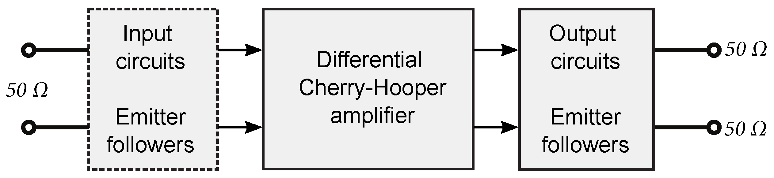
2. Use of a Cherry–Hooper Differential Amplifier
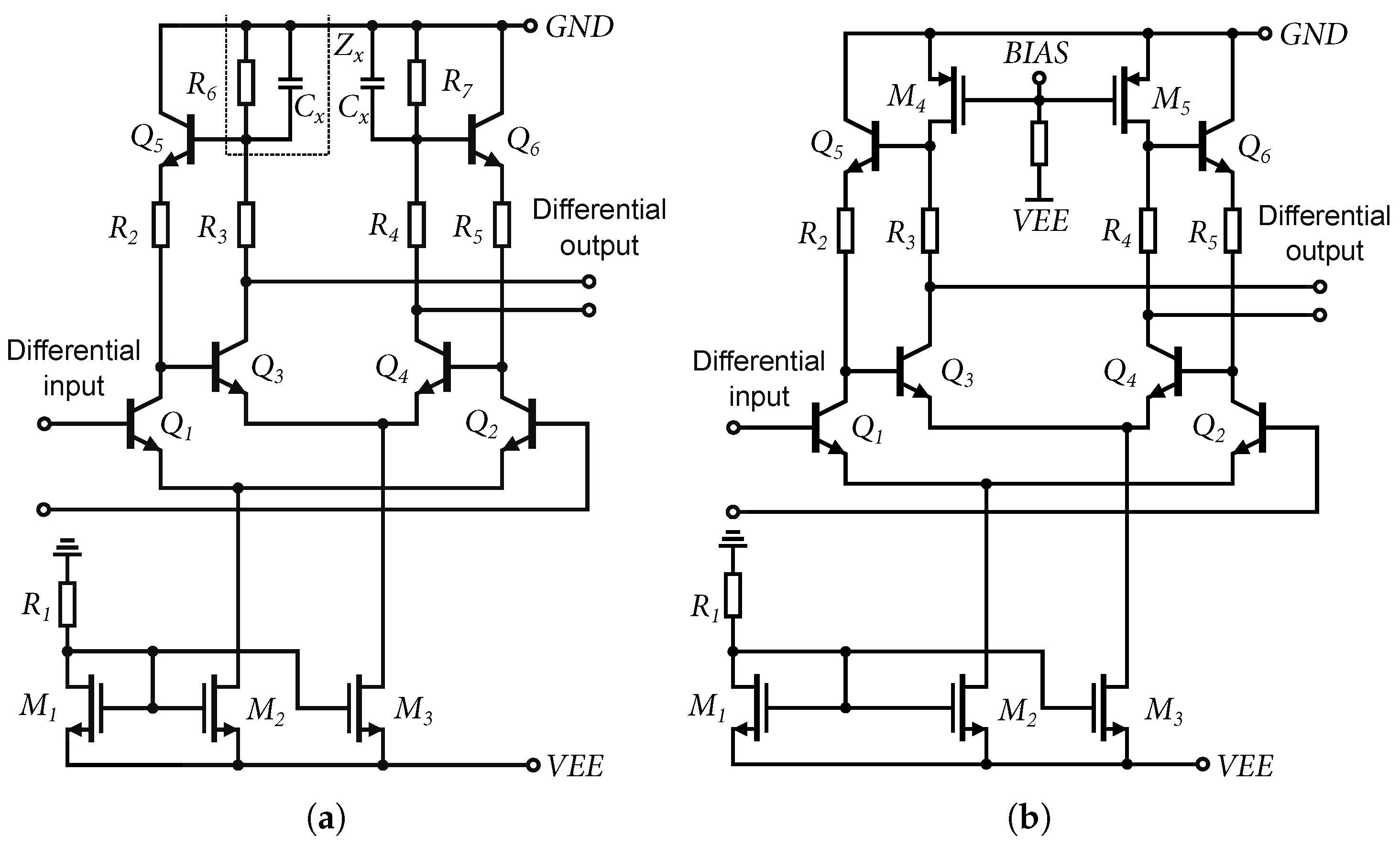
As already mentioned, there are many types of differential amplifiers. Not every type is suitable for a specific UWB sensor system application or a specific semiconductor manufacturing process. Each design represents a compromise regarding certain parameters. In a wideband amplifier, we can consider two interrelated opposing parameters, namely, the bandwidth and the gain of the amplifier. For example, in a simple differential amplifier, increasing the bandwidth leads to a decrease in the gain and the dynamic range. Similarly increasing the gain at a constant supply voltage leads to a decrease in the dynamic range. The Cherry–Hooper amplifier reduces these dependencies because it consists of two amplification stages. The basic structure was designed by E.M. Cherry and D.E. Hooper [
24,
25]. These amplifier stages create an impedance difference between stages [
24]. The structure of the Cherry–Hooper amplifier is designed to ensure that the adjustable gain, the bandwidth, and the dynamic range of the amplifier are less interdependent.
Cherry–Hooper amplifiers are mostly used in applications in digital optical communications [
26], but due to the larger bandwidth compared to a standard differential amplifier, differential amplifiers based on the Cherry–Hooper structure are also promising for use in UWB radar systems emitting the M-sequence. The Cherry–Hooper-type amplifiers described in this paper are primarily designed for special types of directional couplers [
27,
28].
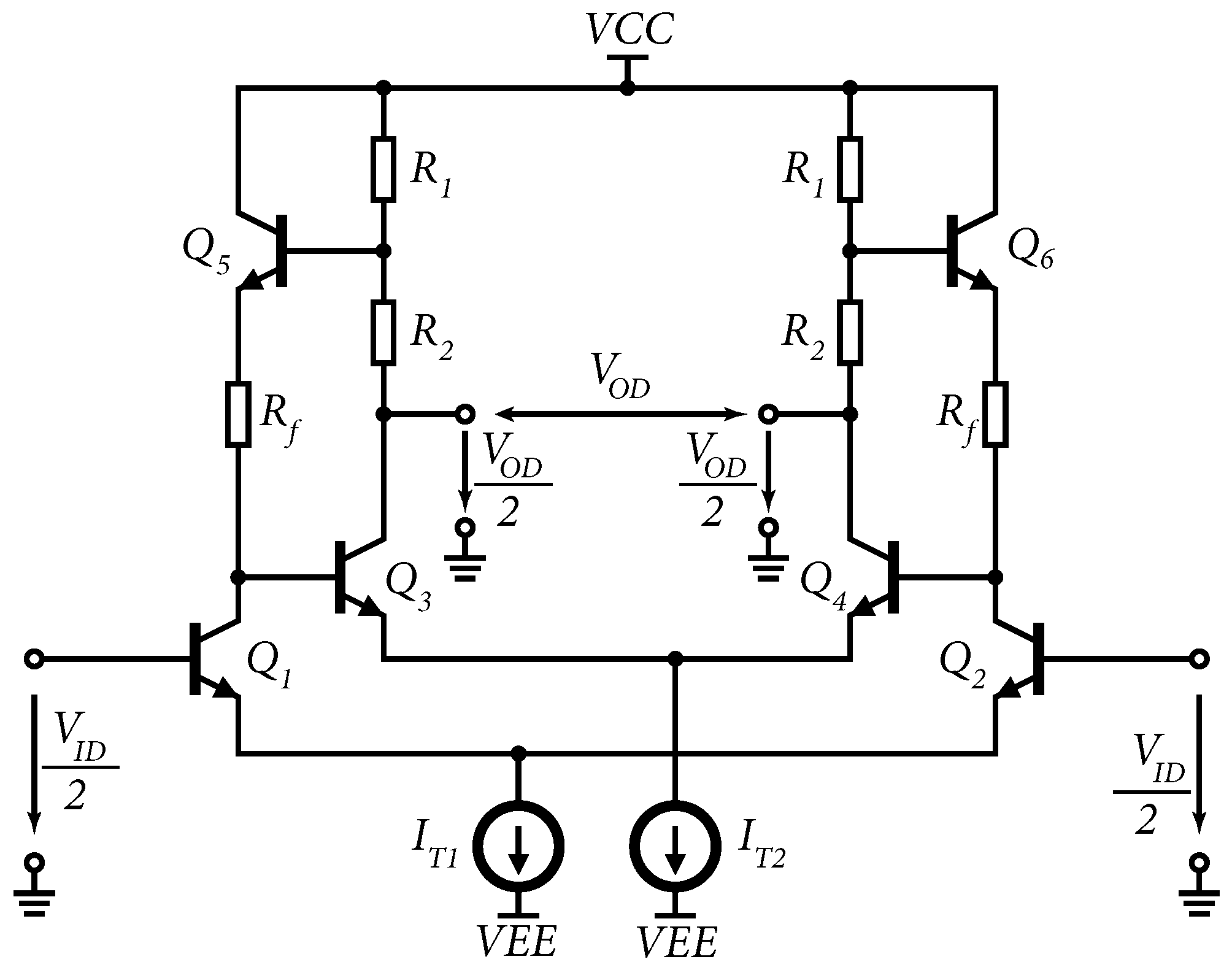
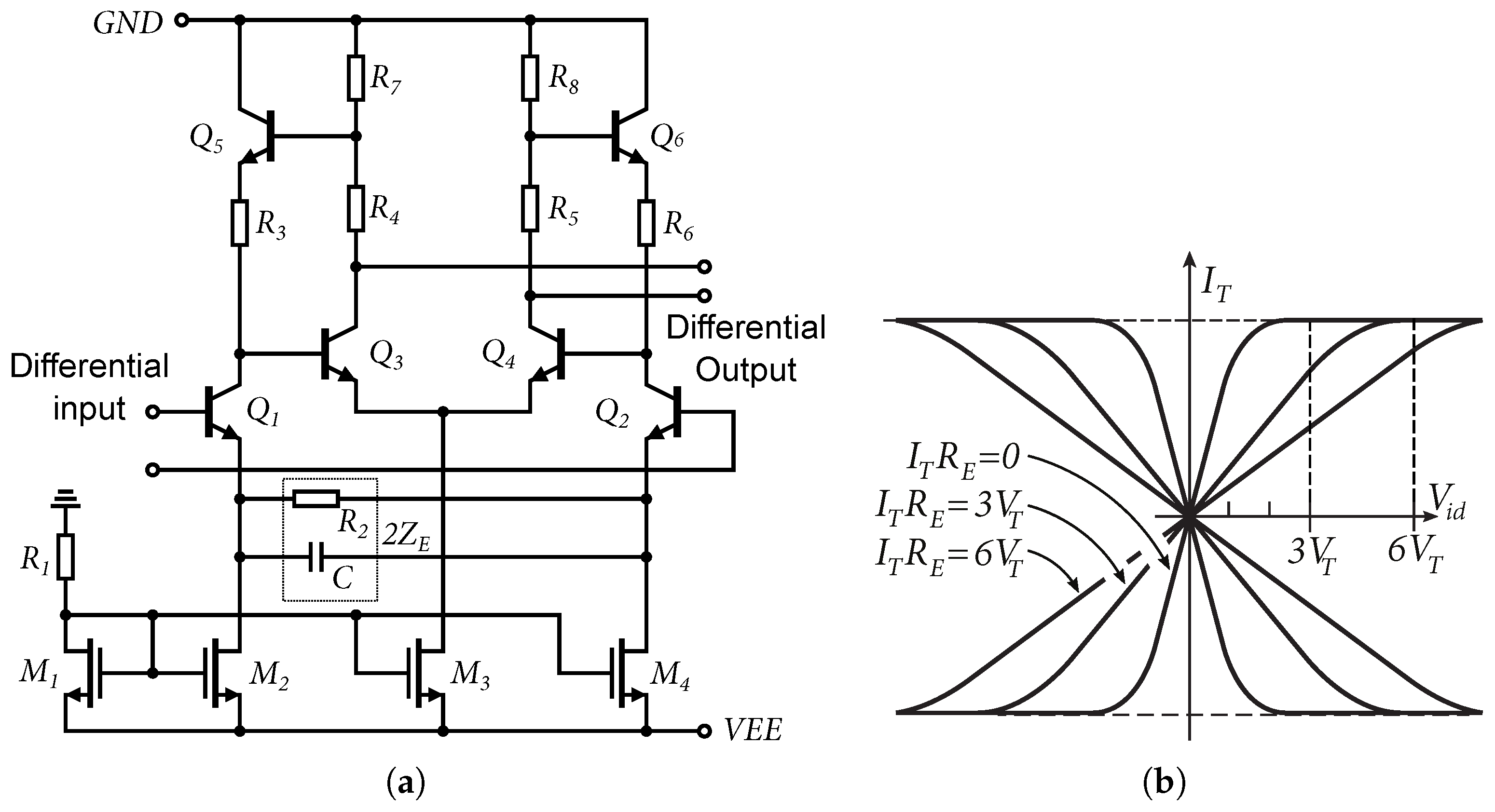
In the original basic structure, simple passive resistive feedback was implemented [
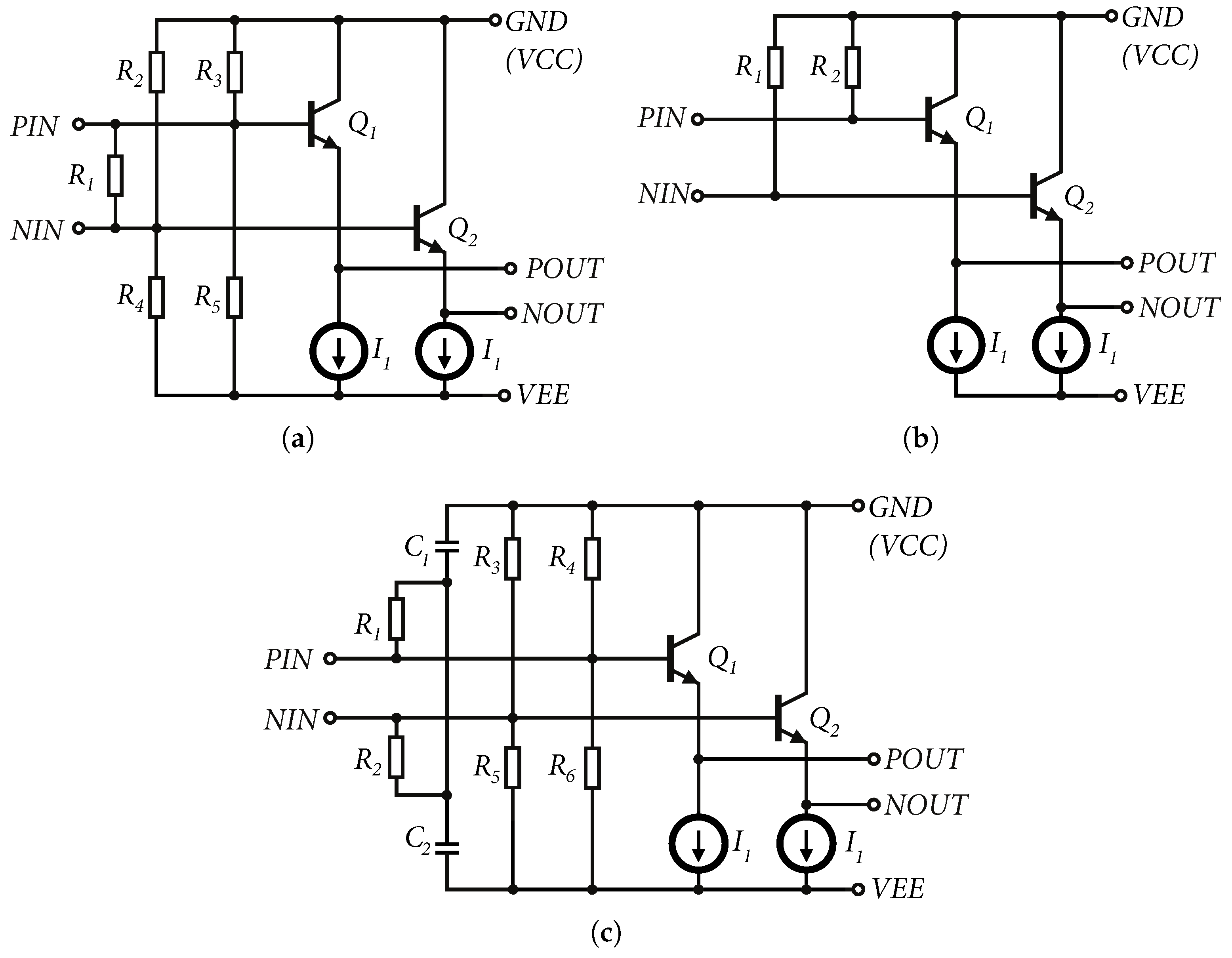
6] but this passive feedback had the disadvantage of loading the output and, thus, reducing the dynamic range of the amplifier. By changing the resistive feedback to feedback created by a unity-gain emitter follower, the impedance decouples the output without affecting the transmission of this feedback. The basic structure of a modified Cherry–Hooper differential amplifier with active feedback is shown in
Figure 1. The replacement of passive feedback with active feedback improves the dynamic properties of the amplifier and reduces the trade-off between the gain settings and the frequency bandwidth, or the frequency bandwidth and the dynamic range. The resistors
and
form a voltage divider for the emitter follower input and, together with the resistor
, set the feedback. The emitter follower is formed by a transistor
(
). This makes it possible to change the gain of the amplifier without changing the resistor
or the current
.
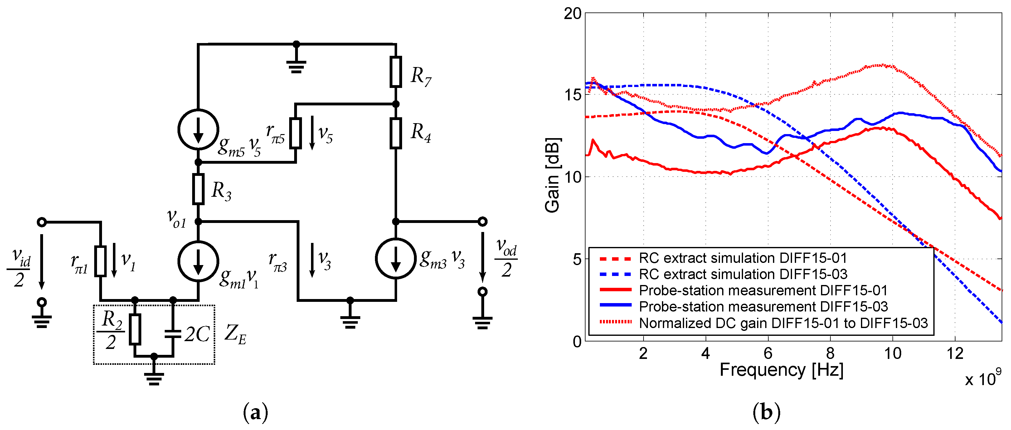
To assess the small-signal gain, the half-circuit equivalent of the proposed amplifier was analyzed (see
Figure 2). By neglecting parasitic effects and simplifying bipolar transistor models, it is possible to determine the gain for small signals of the first
and the second
stage of the differential amplifier:
Equation (
2) shows that by increasing the transconductance of the second stage
or the value of the resistor
, the gain in the first stage is reduced. The resulting gain of the whole differential stage for small signals is given by
. By multiplying Equations (
2) and (
3), the resulting gain is given by:
The gain of the amplifier can be increased by increasing the current
and
, which also increases the output voltage. It is possible to adjust the gain without significantly affecting the maximum output voltage amplitude by changing the ratio of the resistors
and
. Maximizing the amplifier’s bandwidth is possible by changing the ratio of the resistors
, without significantly affecting the gain and dynamic range. A more detailed analysis of the dependence of the individual parameters on the change in resistor values is presented in [
6].
3. Selection of Current Sources
The development of differential amplifiers in integrated form also implies the development and use of suitable current sources. For all the proposed circuits in this paper, current sources with NMOS transistors have been used. When selecting current sources, larger variability in the length/width ratio setting
and lower saturation voltage of NMOS transistors are possible. The advantage of using these is that the NMOS current mirrors are voltage-regulated which eliminates the gain error of the current mirror, as opposed to the current source with current controlled by bipolar transistors [
29].
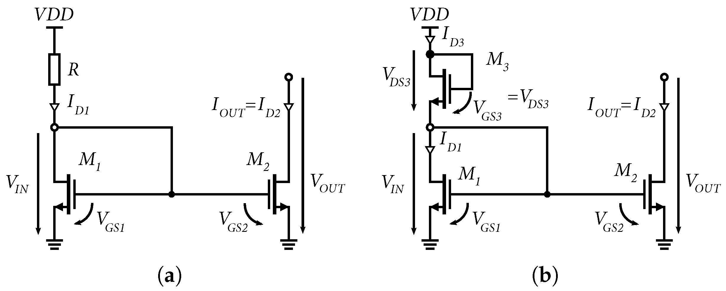
In
Figure 3a the simplest form of the current mirror with NMOS transistors is shown. The transistor
has a gate connected to the drain and operates in a saturation or linear mode depending on the voltage
. If the transistor
works in the active region, then by the voltage
, which is equal to the voltage
, it is possible to control the current
according to Equation [
30]:
where
is the value of transconductance of NMOS and is specified by the production process. The value of
for NMOS transistors in 0.35 µm SiGe BiCMOS technologies is approximately
W is the width,
L is the transistor channel length, and
represents the threshold voltage of the NMOS transistor. 140 µA/V up to 200 µA/V [
29,
30],
If the transistors are the same, i.e.,
, we can assume that:
For the same transistors operating in the active region, the current mirror has a unity gain. In practice, the transistor
and the transistor
may have different dimensions. Using Equations (
5) and (
6), we can determine the ratio of currents with respect to the dimensions of the NMOS transistors as follows:
Equation (
7) shows that the gain of the current mirror can be greater or less than one because the size of the transistors can be varied. The minimum saturation output voltage
of the current mirror with NMOS transistors can be determined by Equation (
8) [
29]:
From Equation (
8), it can be concluded that
depends on the geometry of the transistor and can be arbitrarily small. However, from the technological characteristics of the NMOS transistor, it can be noted that the minimum threshold voltage is defined as
, where
is the thermal voltage [
29], and
. For 0.35 µm, SiGe BiCMOS technology has gate oxide capacitance
and junction capacitance
. Based on this, we can assume that
and
, at room temperature 25 °C.
Nevertheless, there is more variability when adjusting the width of the NMOS transistor compared to the size of a bipolar transistor; in other words, with NMOS transistors at the same current source, we can achieve a lower minimum saturation voltage of the current mirror, which has a positive effect on setting the operating points of the designed circuits.
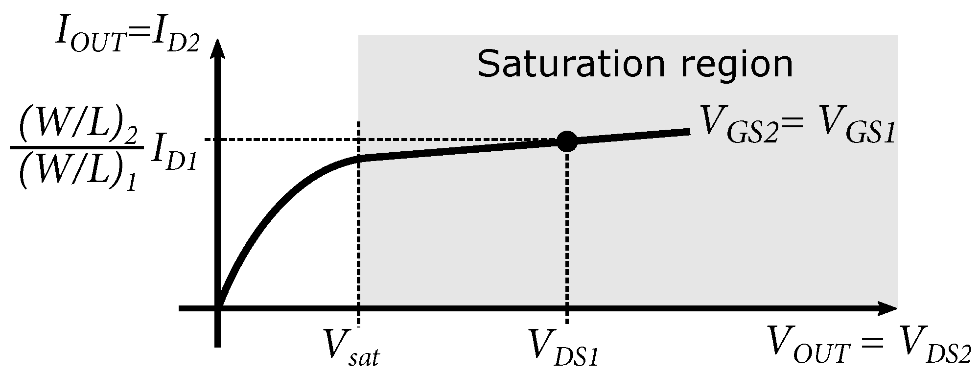
Figure 4 shows the output characteristic of a current mirror with NMOS transistors. It can be seen that if the voltage
drops below the minimum saturation voltage
, the current source drops out of saturation mode and loses its functionality.
As part of the development, the reference resistor
R (
Figure 3a) was replaced by an NMOS transistor
(see
Figure 3b). This had the advantage of saving space when designing the layout of the individual amplifiers. This circuit creates a quadrature voltage divider from two NMOS transistors [
31]. The transistor
operates in saturation mode, which is determined by the condition
, where
is the threshold voltage of the NMOS transistor. The currents
and
flow through transistors
and
in saturation mode and they are equal, given by the equations [
29]:
Modifying Equation (
9) and substituting the variables according to
Figure 3b, we obtain:
If we know the
values of both transistors and the supply voltage
, it is possible from the relations (
9) and (
10) to say that the reference current
and the voltage
can be adjusted using the width-to-length ratio of the transistors
and
. From the above theoretical analysis of the NMOS current mirror and referring to [
29,
30], it is possible to say that current mirrors with NMOS transistors provide greater setup variability at small supply voltages and provide lower saturation voltage values compared to bipolar transistors. Another advantage of current mirrors built from NMOS transistors is the possibility of connection of multiple outputs without degrading the mirror gain, as is the case with bipolar mirrors; thus, it is possible to drive several outputs with many times larger transistors using one small NMOS. Based on this analysis, it can be said that current mirrors based on NMOS transistors are better suited for practical applications in BiCMOS technology.
4. Input and Output Matching Circuits
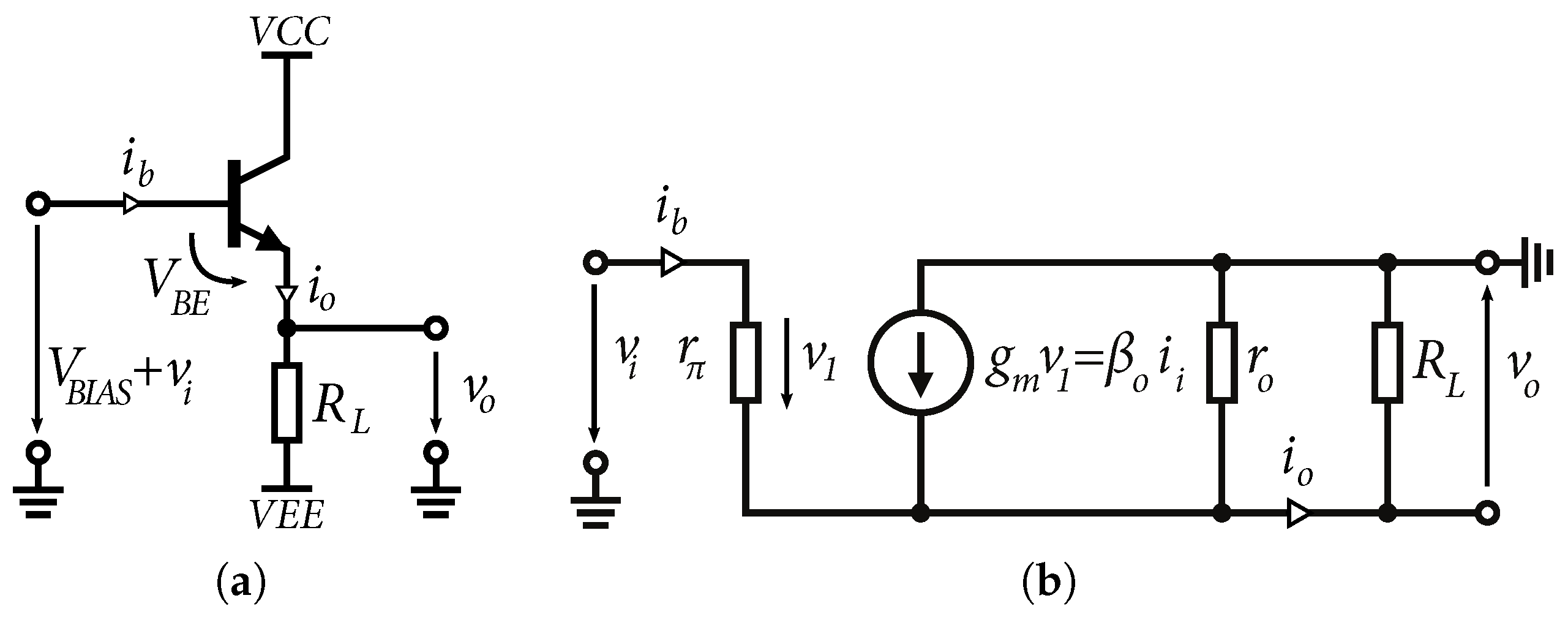
For high-frequency and wideband applications, the input and output matching of the circuits is very important. Matched inputs reduce losses and also reduce standing waves due to mismatch [
32]. Emitter followers are extensively used as input and output circuits. The common identifying feature of this circuit is that the signal is applied to the base and the output is taken from the emitter. A basic schematic of the emitter follower is shown in
Figure 5a. In terms of signal integrity, the output signal is identical to the input signal, but shifted by the DC value of the voltage
VBE. Because the voltage
VBE is a logarithmic function of the collector current
IC, the base-emitter voltage
VBE is almost constant, although the collector current varies over a larger range. An equivalent small-signals model is shown in
Figure 5b. The emitter follower is characterized by a unit voltage gain, which can be based on the conditions
and
[
29] expressed as:
where
RL is the value of the load resistance or the output resistance of the current source.
It is also possible to approximate the input resistance of the emitter follower
by replacing the voltage source with a current source
. The resulting input resistance can be expressed as [
29]:
Based on Equation (
12), it can be said that the emitter follower is characterized by high input resistance, which is given by the base resistance
and output resistance multiplied by the current gain
of the transistor. The advantage of the high input impedance in order units of kΩ of the emitter follower is that it is possible to adjust the input impedance using resistors according to the requirements of the high-frequency circuits. In
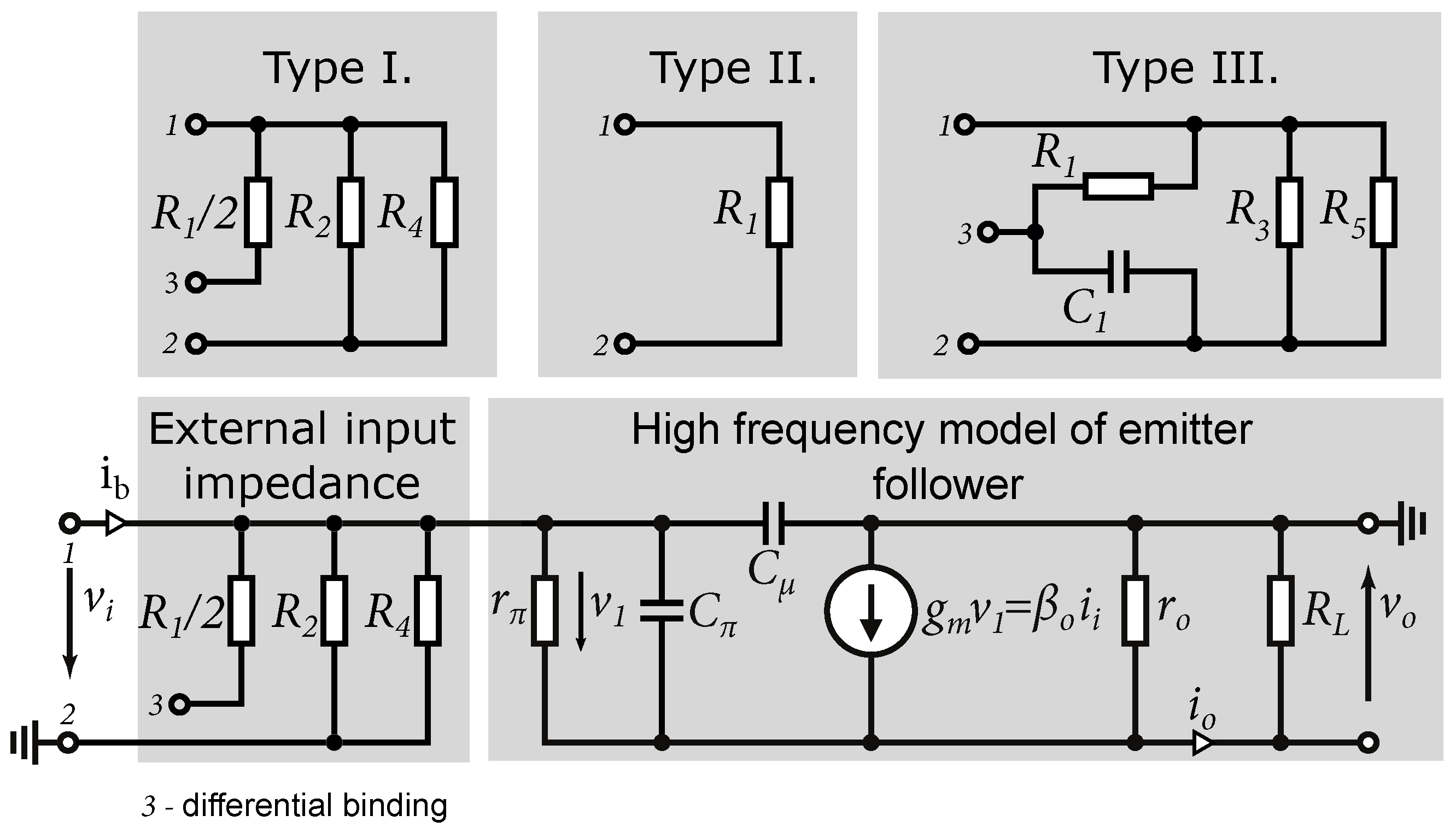
Figure 6a–c are shown the input circuits used in the design of the wideband amplifiers described in this paper. Based on the small-signal equivalent circuit, we can approximate the input wideband impedance of all three inputs. A small-signal equivalent schematic for wideband signals is shown in
Figure 7.
Input impedance
of the emitter follower based on Equation (
12) and
can be expressed as [
29]:
where
represents the input capacity of the emitter follower:
The resulting differential and single-ended input impedance values can be approximated as a parallel combination of the emitter follower input impedance and the impedance defined by the type of external circuit.
Input matching type I is used to set the input differential impedance regardless of the single-ended impedance. Resistors
, as shown in
Figure 6a, have values of the order of
so that they do not create additional power consumption and are intended to set the operating point of the next amplifier. Using resistors
, this operating point is set to the approximate center of the input range of the amplifier. To set, the operating point must be offset by
VBE. The resistor,
Figure 6a, adjusts the differential input impedance of the amplifier for a particular application. This input matching has been used for amplifiers designed for wideband directional couplers, where the input differential impedance was set to
. This type of input is suitable only if differential signaling is assumed. In this case the nominal value of the input impedance is set to
[
3].
The input matching type II is the simplest in terms of circuitry, as shown in
Figure 6b. It consists of two resistors
and
, which are directly connected to the ground. In this case the input single-ended impedance for each of the inputs is set. The differential impedance is
. This type has the advantage that the single-ended impedance value for each input is set at the same time, as is the differential impedance between the inputs.
Another advantage is the wideband capability; in this case, we can start at the DC signal up to high frequencies. The disadvantage is the direct connection of
and
to the ground, which, in terms of operating point settings, may not suit the next amplifier settings. Sometimes it is necessary to connect up to two emitter followers in a row to achieve a shift in DC voltage from input to output by
. Another disadvantage is that it requires a symmetrical or negative supply voltage in order to create an operating point to operate the transistors in active mode. In the case of positive supply only, the input impedance is tied to the supply
VCC and coupled to
GND through the bypass capacitors in the circuit, which can cause different unwanted crosstalk and current loops in the circuit. The input matching type II was used in the input amplifier for the clock signal in the designed 7-bit ADC [
22].
Input matching type III combines the advantages of type I and II. The circuit in
Figure 6c maintains the operating point setting; i.e., using resistors
, it is possible to adjust the DC input voltage as required regardless of the type of power supply. The differential impedance is set by a series connection of resistors
and
. Ideally, i.e., after neglecting the input impedance of the emitter follower and the parasitic properties of the chip, the differential impedance in such an arrangement is constant and independent of frequency. The single-ended impedance of each input coupled to the ground depends on the value of
and
and the capacitances of
and
, respectively. In this case, the capacitances
and
represent a “short-circuit” for the high-frequency signal. The disadvantage of such wiring is that the non-differential matching of inputs depends on the size of the capacitances
and
. Within the chip design, it is possible to use capacitances of sizes of the order of units of pF, allowing single-ended input matching at the start frequencies of the order of hundreds of MHz to units of GHz. Such wiring can be used for applications that require input signals higher than hundreds of MHz, for example, clock or mixer input. However, it is possible to lead a contact from the chip to connect the capacitances and supplement these capacities with an external off-chip capacity. This will improve matching to units of MHz but will increase the number of external components around the chip.
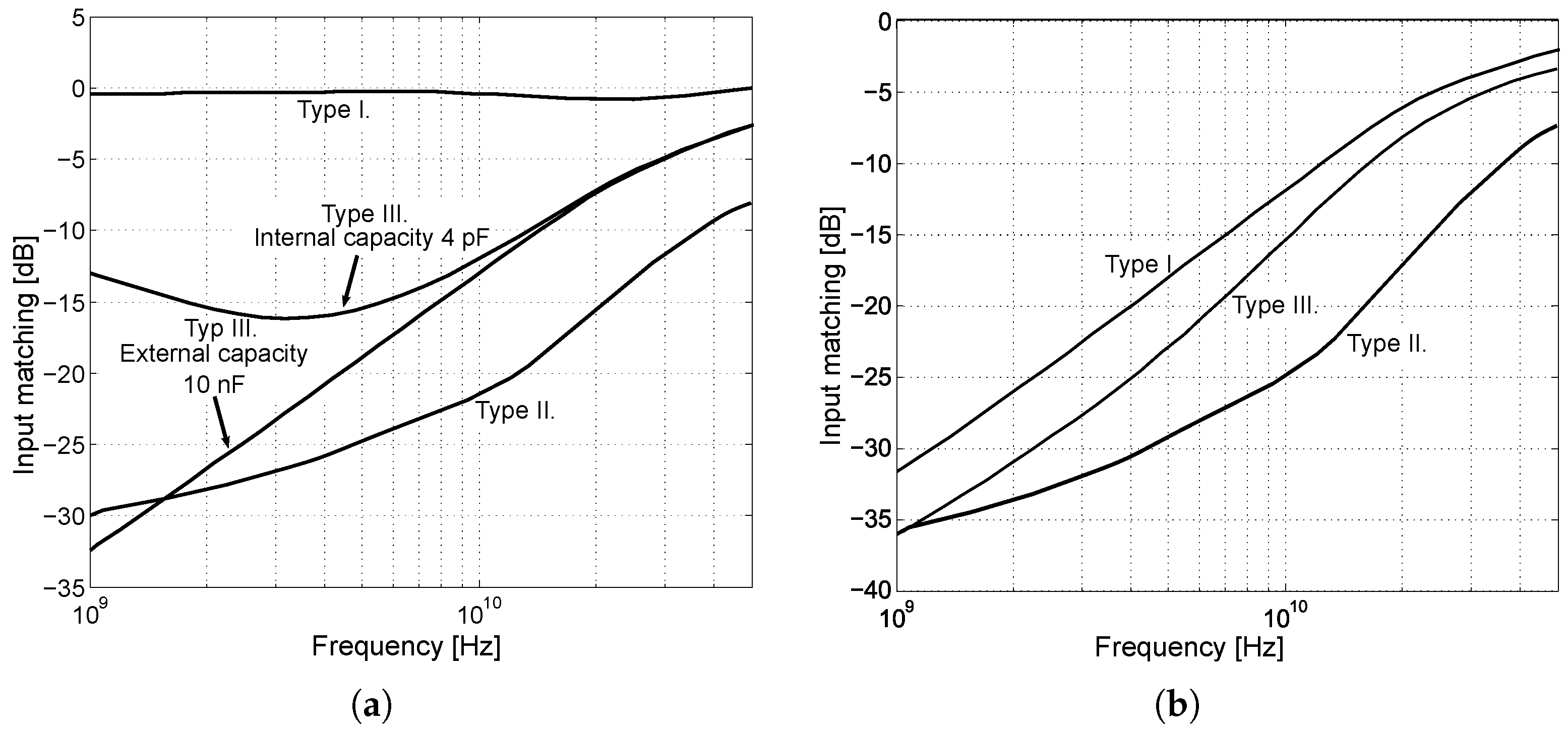
A comparison of input matching of different types of input circuits is shown in
Figure 8b. The comparison represents a schematic simulation without the influence of the parasitic effects of the chip.
Figure 8a shows the single-ended
input matching. It can be seen that in the case of the first type, the input is not matched. In the case of the second type, the obtained matching is the best one. The input matching of the third type depends on the size capacities of
and
. From
Figure 8a, it can be seen that the differential matching to
is almost identical in all three cases. The small differences are due to different input transistors. In the case of Type II, four times smaller transistors were used compared to Type I and Type III, which have smaller parasitic capacitances and result in better matching at higher frequencies. From the input impedance calculation and the compared characteristics, it can be seen that the emitter follower shows capacitive behavior. When using larger input transistors, the mismatch at high frequencies increases. Therefore, a choice must be made between a trade-off of transistor size, input matching, and the output current of the resulting circuit, i.e., the ability to excite the next stage.
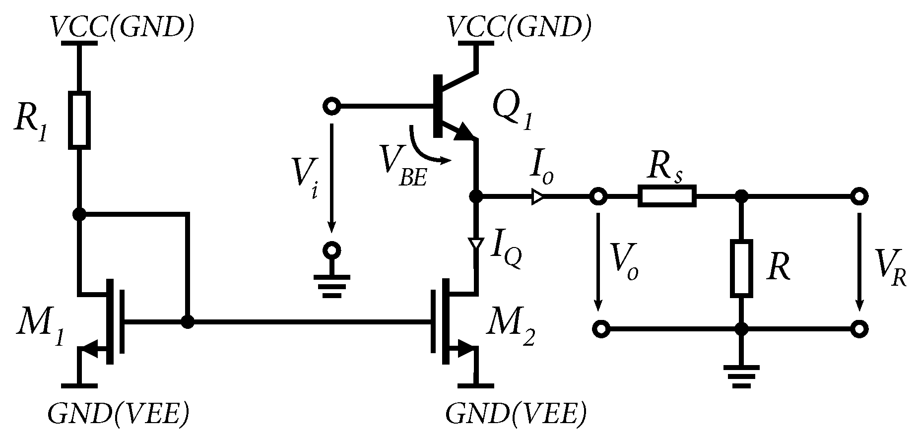
The ability of the emitter follower to excite other circuits is predetermined by its low output resistance. Therefore, emitter followers are also used as output stages. The emitter follower is used as an “impedance transformer” with high input and low output resistance.
Figure 9 shows the use of emitter followers as the output stage in differential amplifier designs.
The circuit can be powered by negative voltage determined by
VEE and
GND, positive voltage determined by
VCC and
GND, or a symmetrical voltage determined by
VCC and
VEE. The emitter follower is controlled by a current source consisting of NMOS transistors. The output resistance of the emitter follower on the schematic for small signals in
Figure 5b if
can be determined as follows [
29]:
where
represents the resistance of the current source. Equation (
15) shows that increasing the current of the current source increases the gain of the bipolar transistor
and decreases the output resistance of the transistor,
and
of the current source, thus decreasing the total output resistance of the emitter follower. In our case, for 0.35 µm BiCMOS technology, using the standard NPN transistors with a current gain factor of approximately
and a current source
mA, the emitter follower achieves an output resistance of about
. The output stage should also provide a large output voltage swing without distortion. This means that for proper excitation of other circuits, the operating point of the emitter follower has to be set so that the output signal is not clipped by saturation of the transistors
and
,
Figure 9.
The transmission characteristics of the emitter follower as an output stage based on the assumption
are shown in
Figure 10a. The emitter follower is driven by the voltage
, which is offset by the DC offset value
VBE, so that the DC component of the output voltage
is approximately at the center of the DC characteristic. From the positive part of the conversion characteristic, the output voltage is limited by the saturation of the transistor
. In the negative part of the transfer characteristic, the output voltage is limited by the magnitude of the load
R and the current
of the current source. Increasing the current
will increase the voltage swing across the load
R, which is limited by the voltage
. On the other hand, decreasing the resistance
R will increase the load and, thus, limit the output voltage swing, which can be seen at the bottom of the characteristic in
Figure 10a.
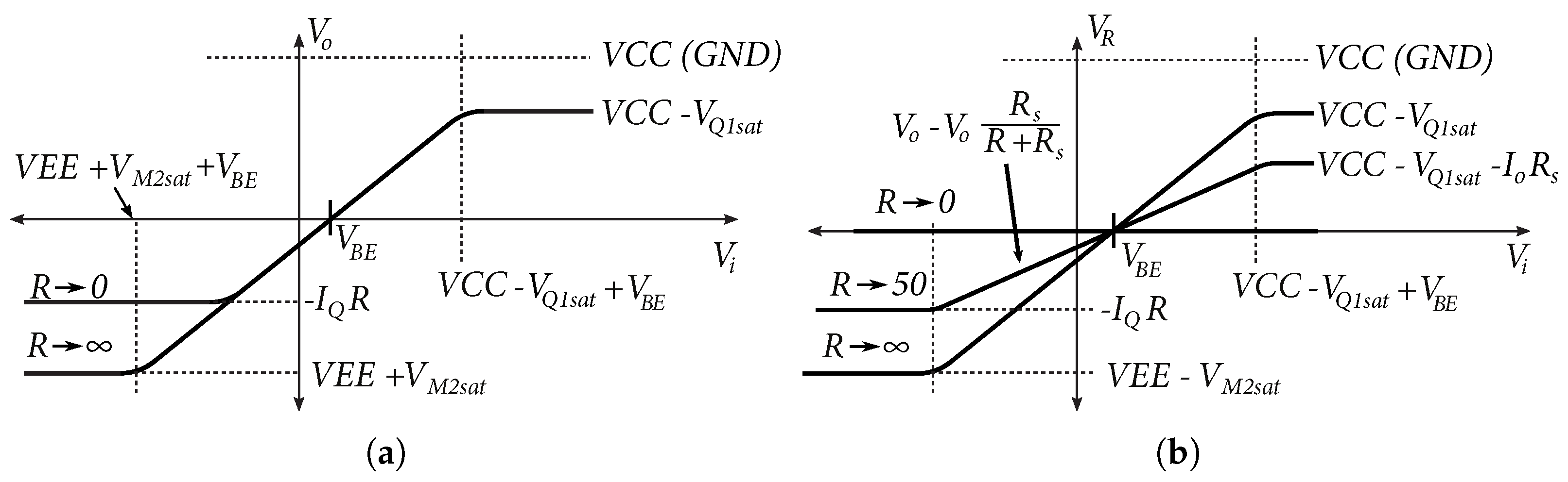
From Equation (
15) and simulations created in 0.35 µm BiCMOS technology, the output impedance of the emitter follower was determined to be of the order of
units. In a
environment, this output impedance is not suitable, therefore, a resistor
was added to the series. For correct matching, the total output resistance must be equal:
The resulting conversion characteristic of the output voltage
to load
R is shown in
Figure 10b. In the case,
, the output voltage
. In other cases, the output voltage
is given by:
If the total output impedance of the output is equal to the load, the resulting voltage at the load is a half.
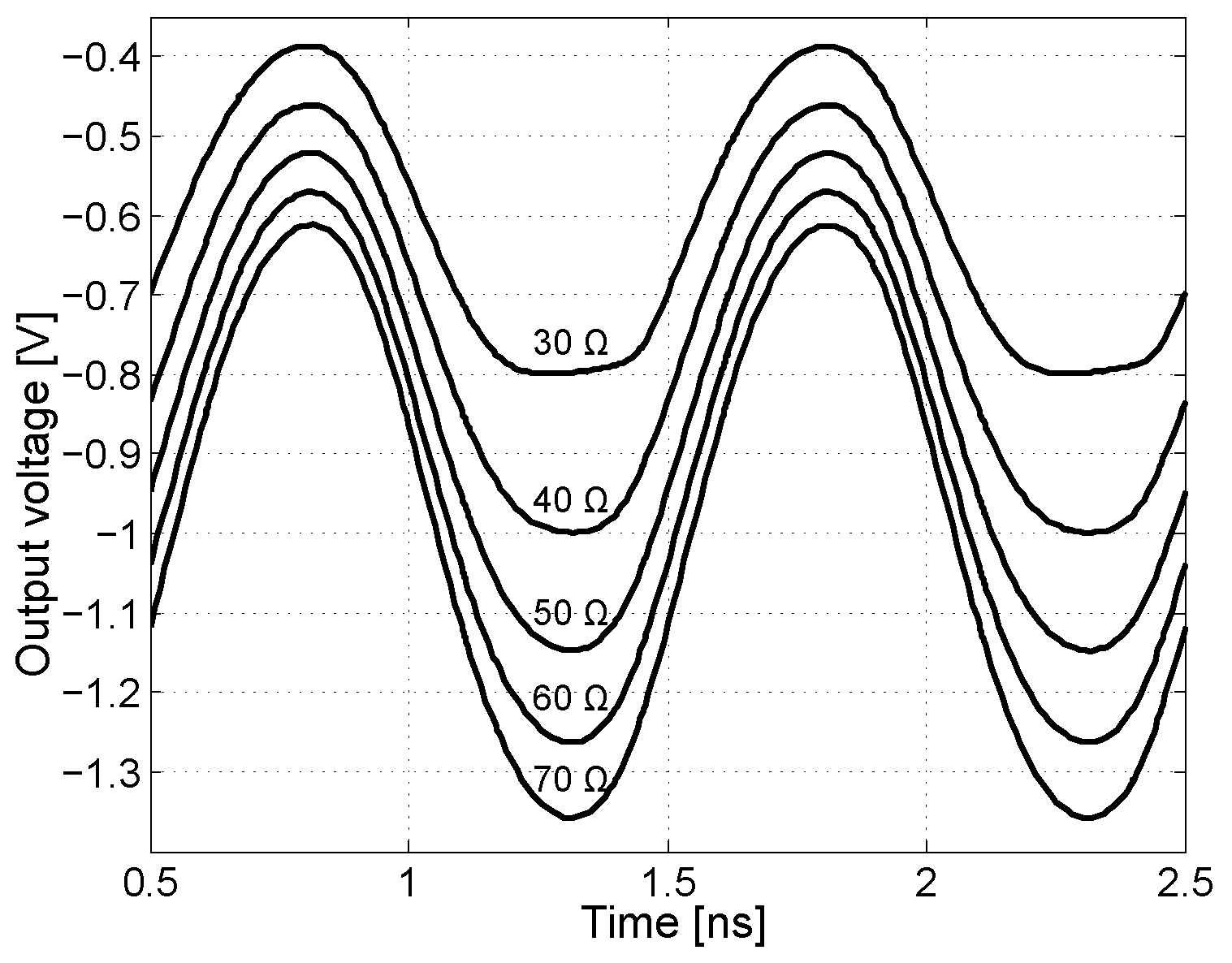
Figure 11 shows the output sinusoidal waveform with a total output impedance of
of the emitter follower with different load impedances, at a signal frequency of 1 GHz. It is also worth mentioning the output impedance of the emitter follower and the circuit behavior under capacitive loading, including the NMOS transistor in the current source. The presented output resistance of the emitter follower (
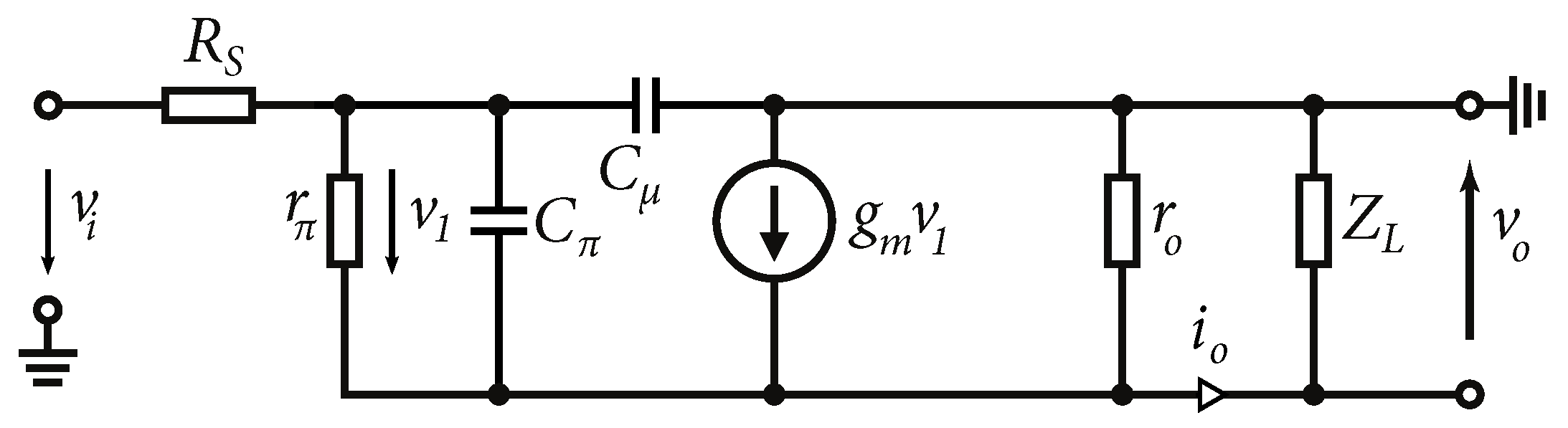
16) is valid if the signal frequency
. The model for calculating the output impedance of the emitter follower for high frequencies is shown in
Figure 12. The resistor
represents the output impedance of the signal source.
At high frequencies,
can short the resistor
. Neglecting the effect of the capacitance of
, we can approximate the output impedance as [
29,
33]:
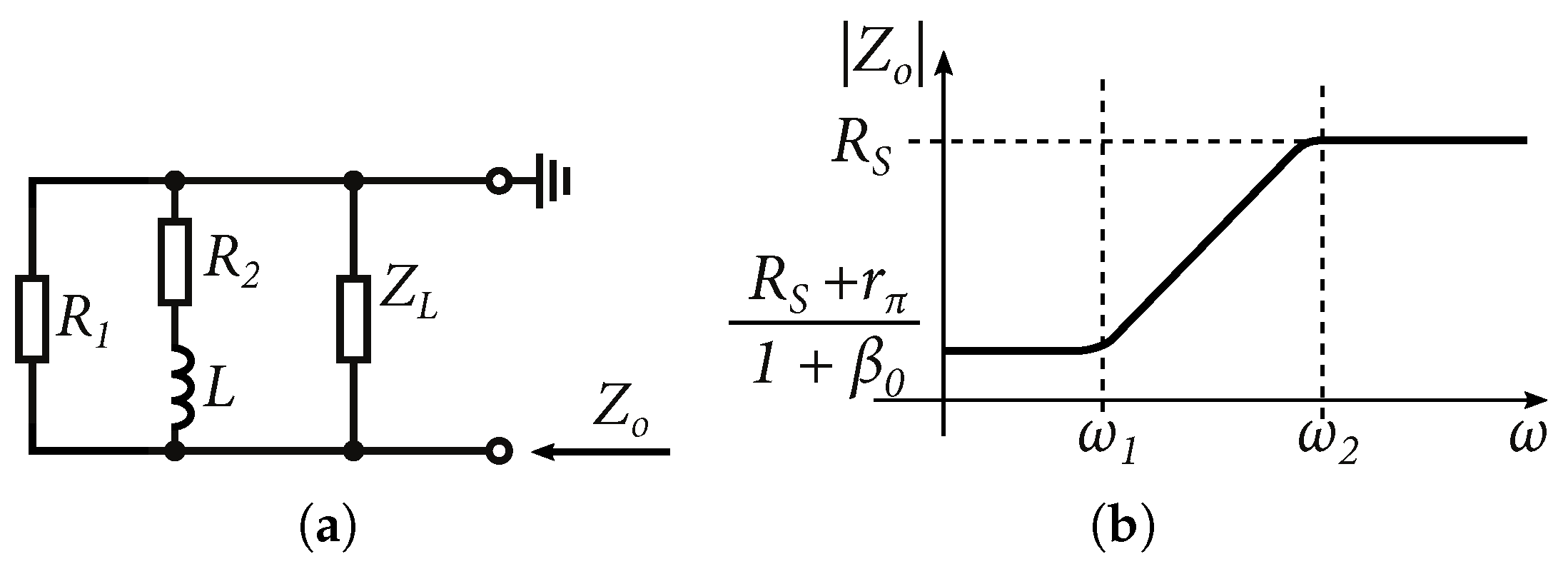
Based on the schematic in
Figure 12 and the characteristic in
Figure 13b, it is possible to say that the output impedance
of the emitter follower at high frequencies shows inductive behavior. Where the frequencies of
and
are [
33]:
An alternate schematic of the output impedance is shown in
Figure 13a. If we assume that the load impedance of the emitter follower
is also capacitive, the following results in a parallel resonant circuit, where [
33]:
where
represents the DC output resistance of the current source (NMOS transistor
Figure 9) and
represent the parasitic capacitances of the NMOS transistor
and possibly other parasitic capacitances of the circuit that are excited by the emitter follower.
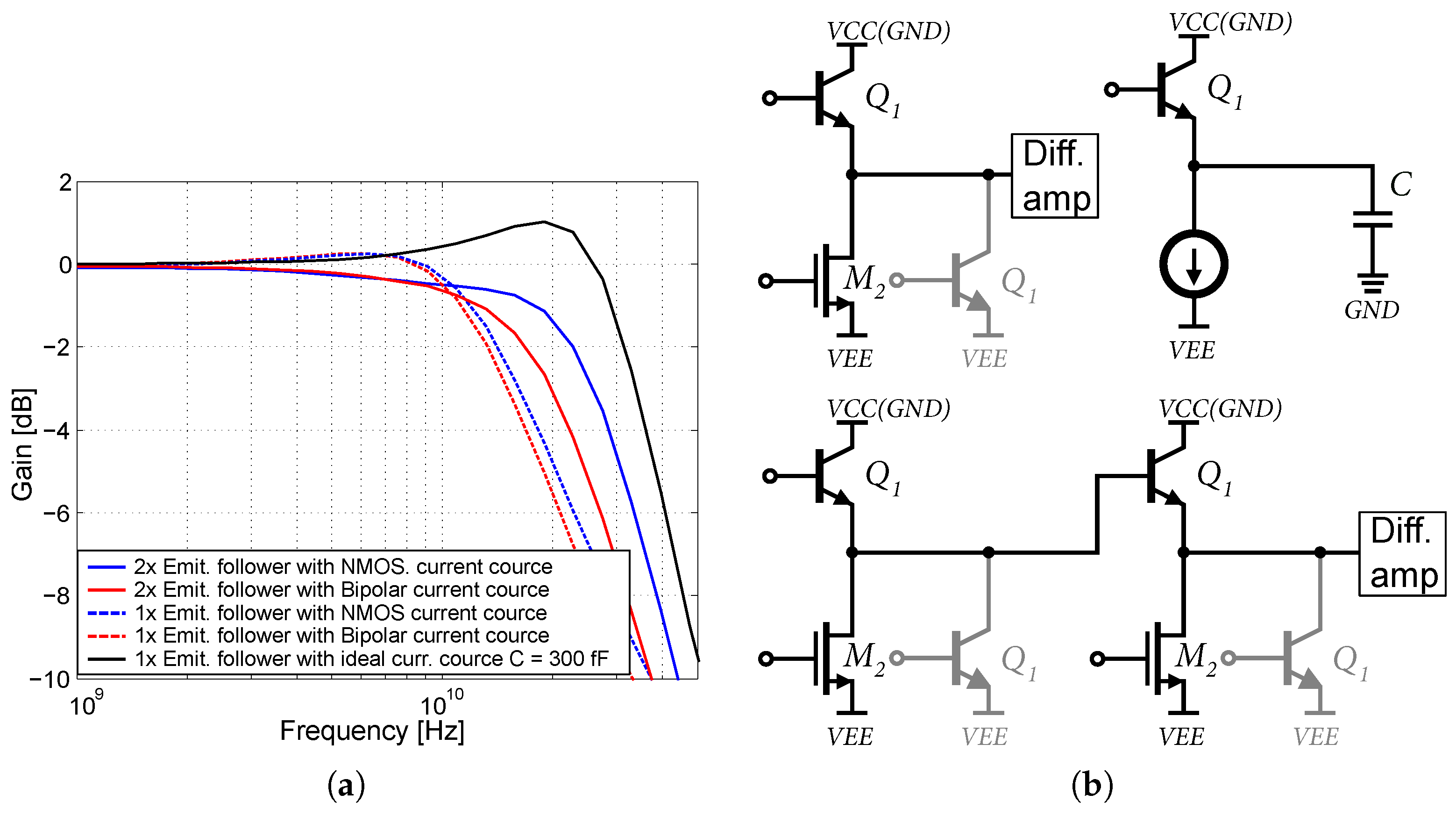
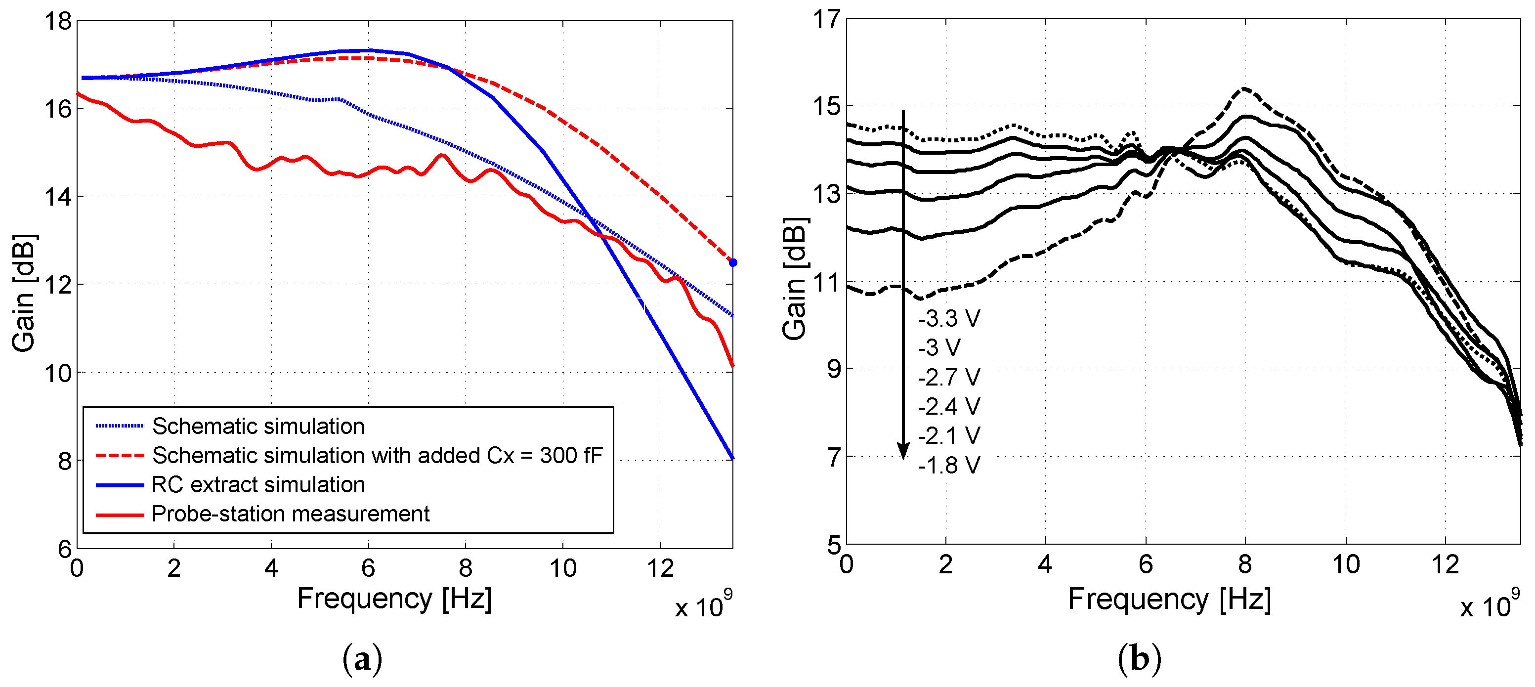
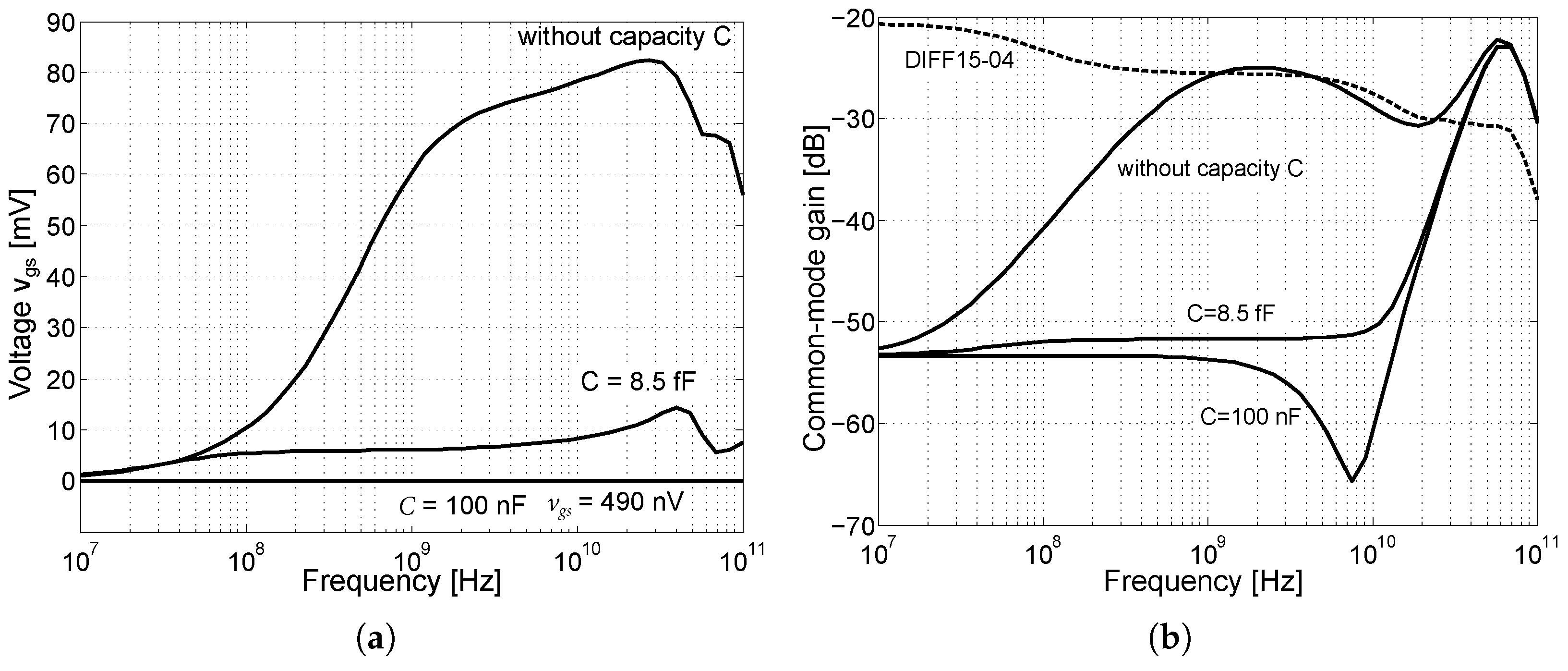
Figure 14a shows the simulation results in 0.35 µm BiCMOS technology according to the scenarios in
Figure 14b. Three scenarios were created, where the emitter follower was loaded with an NMOS and a bipolar current source with an attached differential amplifier.
The third scenario represents an emitter follower with only an ideal current source, loaded with artificial capacitance. It can be observed that the bandwidth of the emitter follower with the NMOS current source is larger, along with the cascading of two emitter followers with the NMOS current source. With the emitter follower loaded with an ideal current source and a capacitance of 300 fF, it is possible to observe a gentle resonance and gain increase. By using emitter followers with NMOS current sources or cascading them, it is possible to increase the bandwidth of differential amplifiers. The input and output matching were simulated with SP analysis in the CADENCE Virtuoso design environment with ideal 50
connected to the amplifier. This simulation was performed using RC-extract and approximate wire-bond induction. The input and output matching resistors were tuned using a Smith diagram and an S11 linear graph. The simulations were conducted at a set temperature of 27 °C. For more information about the transmission characteristics of the emitter follower, see [
29,
30,
33].
6. Evolution of Layout and Comparison
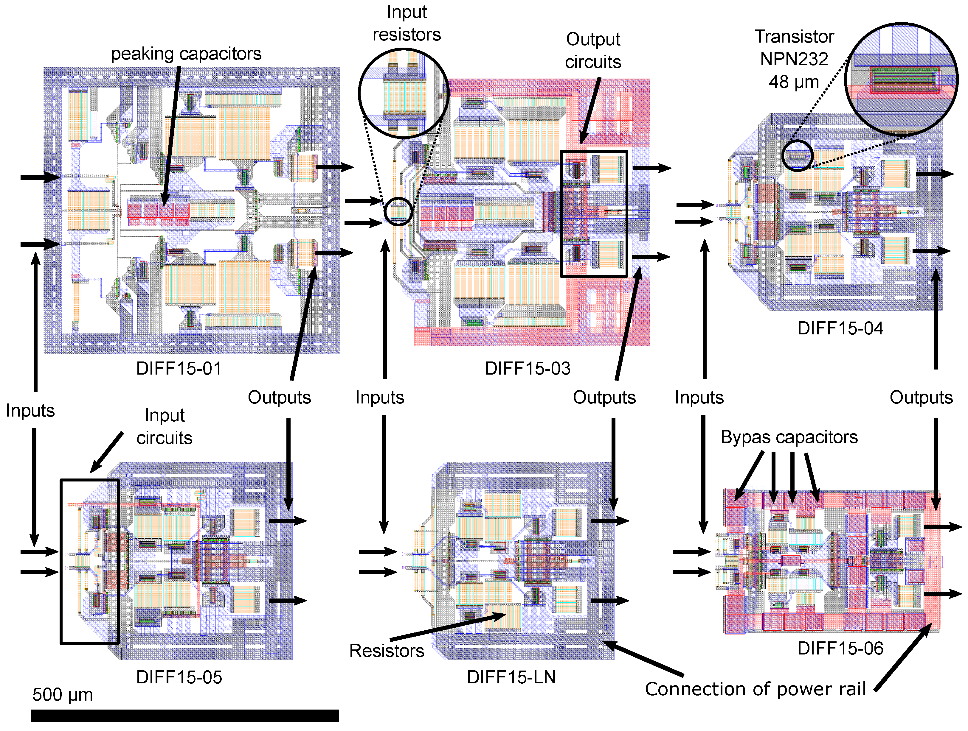
With the development of the schematic circuits of amplifiers, the layout of the elements on the chip, i.e., the layout of the individual parts of the amplifiers, also evolved.
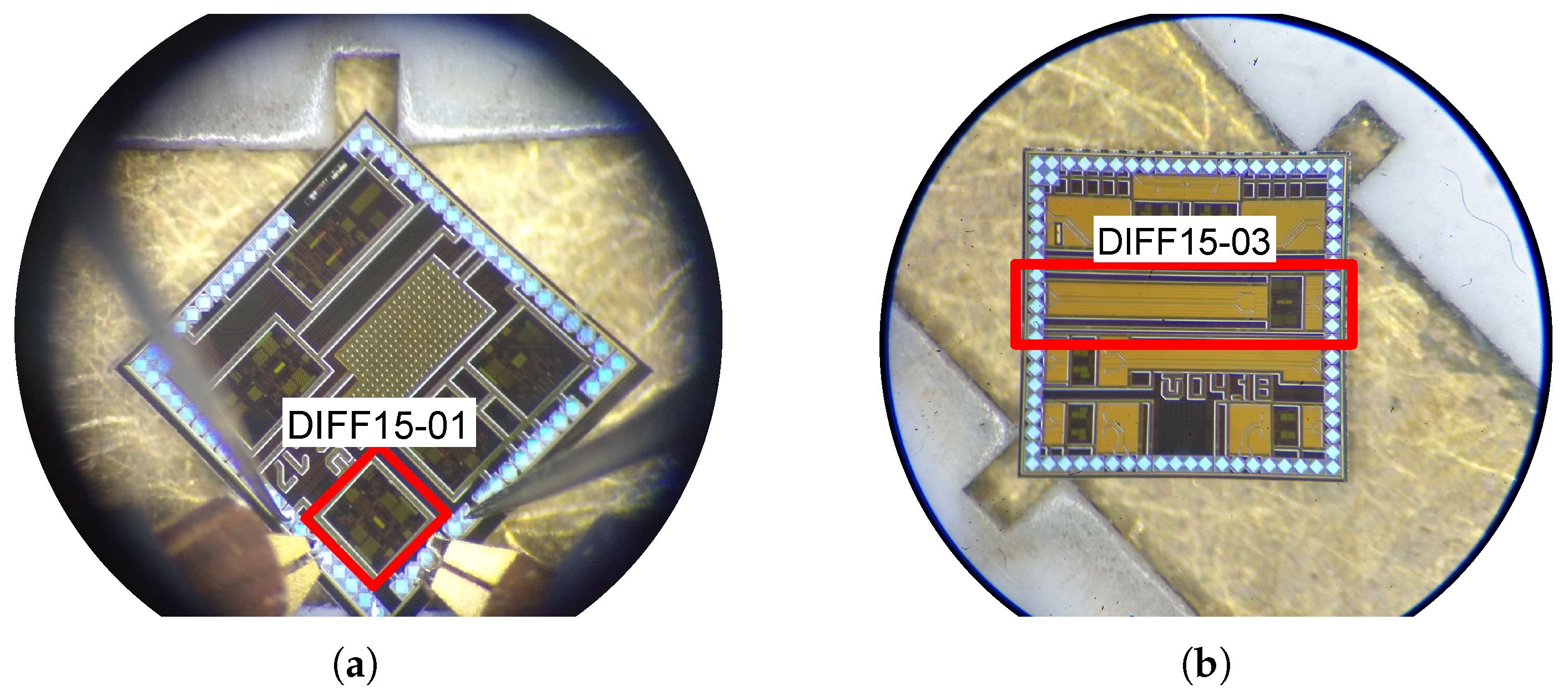
Figure 28 shows detailed layouts of the presented differential amplifiers, designed in the CADENCE Virtuoso design environment. The view is to a uniform scale for better interpretation of the amplifier size. The amplifiers were designed and fabricated in 0.35 µm SiGe BiCMOS technology from the Austrian manufacturer AMS.
In the layout (
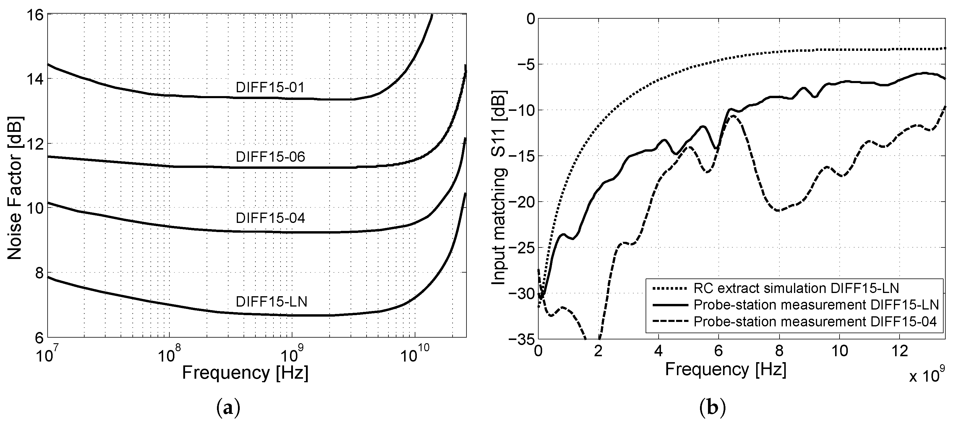
Figure 28), a reduction in the area occupied by individual cells is visible. The amplifiers were designed with structures as symmetrical as possible to keep the best differential parameters. The DIFF15-01 amplifier was the largest, with more than twice the surface area of the DIFF15-06 amplifier. The biggest problems with the DIFF15-01 amplifier were high power consumption and miscalculation of the current density of metallic interconnects and the vias between the layers, and longer leads due to the cell size. This caused a reduction in the low-frequency gain. The amplifier was designed for a gain of 15 dB, but only achieved 12 dB.
The overall power consumption and cell size were reduced by removing the cascade of the two emitter followers. For the other designs, wider metallic interconnections were used, and they were drawn parallel to each other on two layers. The vias between the layers were increased. Additionally, reducing the size of the resistors to the edge of the current density also contributed to a reduction in the amplifier cell size. In 0.35 µm BiCMOS S35D4M5 technology, the minimum length/width ratio of resistors is 5:1.
The smaller resistor area also achieved a reduction in the parasitic capacitance, which contributed to increased bandwidth and better input-output matching at higher frequencies. Some types of resistors offer a double row of connection via, to reduce the transient resistance and more precise adjustment. The wider and shorter signal junctions between transistors were used which, in the context, represents a lower transient resistance of the individual interconnections. This resistance connection with the parasitic capacitance represents a low-pass filter. The latest design of the DIFF15-06 amplifier surrounds power capacitances that help bypass current spikes, and has capacitances for the current source that improve CMRR.
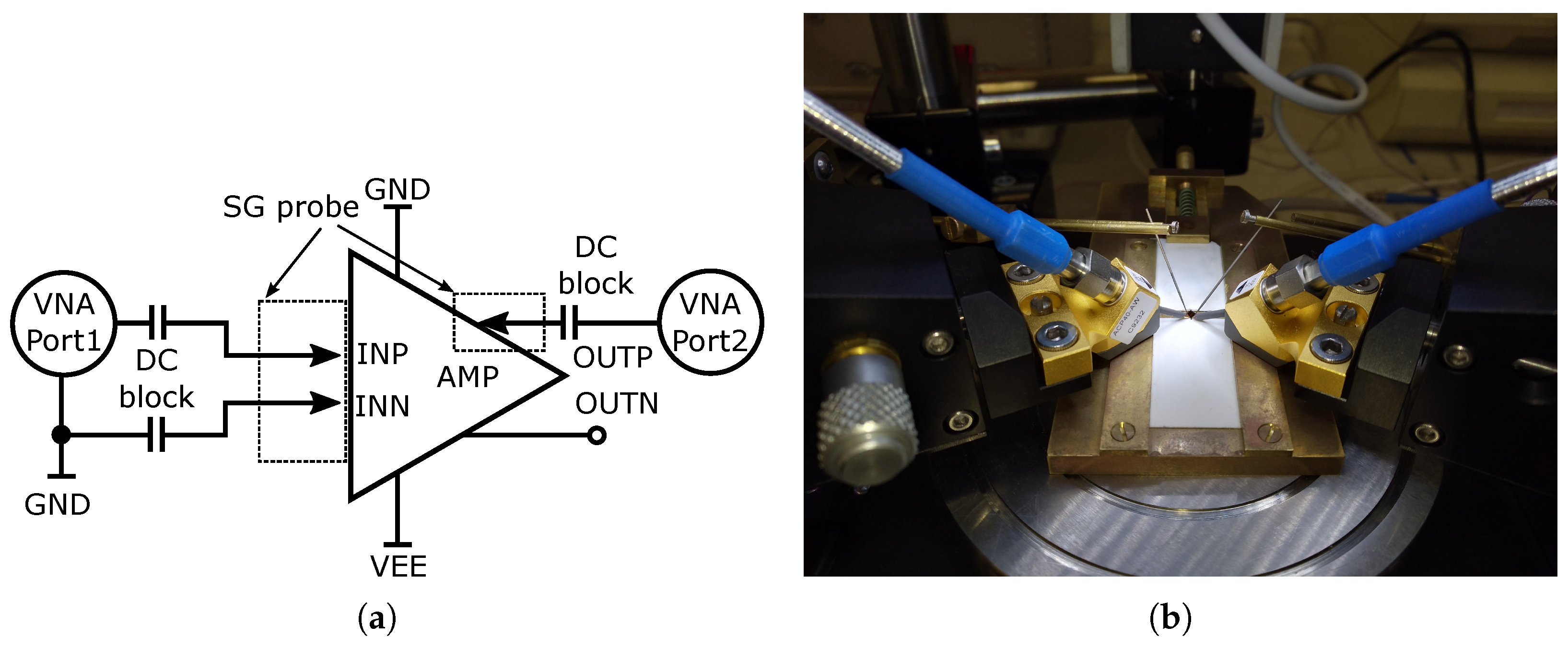
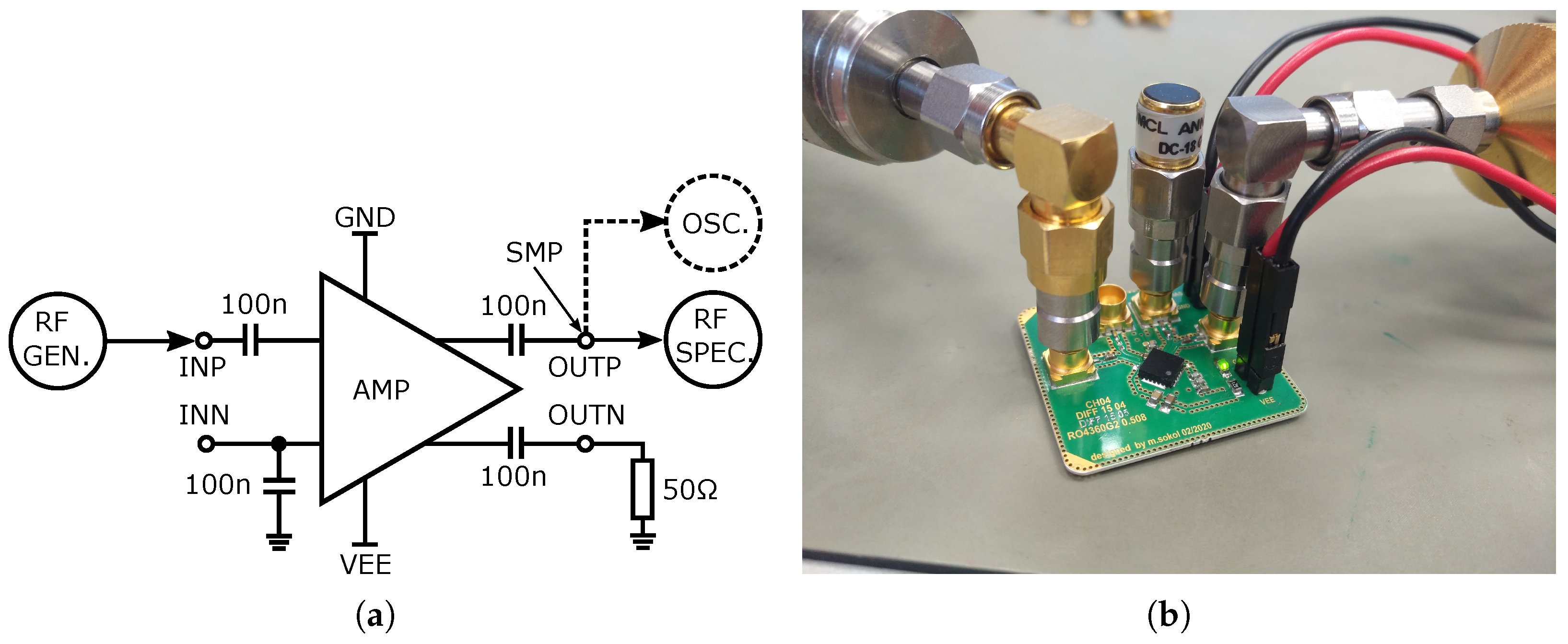
The presented characteristics are the result of measuring the amplifiers using a probe-station. A block diagram and photo of the probe-station measurement setup are shown in
Figure 29. For S-parameter probe-station measurement, an Agilent PNA-X N5241A vector analyzer with maximum frequency 13.5 GHz was used. Two types of micro-probes, namely, a CASCADE MICTROTECH ACP40-AW-SG-100 with 40 GHz bandwidth and an MPI TITAN T26V-SG0100 probe with 26 GHz bandwidth, were used. Because the probes are only in an SG (signal–ground) configuration, a quasi-differential connection was applied with a PE8212 inner outer DC-block capacitor so that the probe could be connected to the differential input with 50
. At the output, only a standard DC-block capacitor was used. The second output of the amplifier was unconnected and unmatched due to space limitations and no possibility to connect another probe. Such a probe-station best describes the actual parameters of the amplifiers as they are not affected by wire-bonding, packages, and PCBs. The compression point and output voltage swing was measured on a wire-bonded and assembled amplifier on PCB. A block diagram and photo of the PCB measurement setup are shown in
Figure 30. For compression measurement, a signal generator Keysight N5183B and an Agilent N9020A spectrum analyzer up to 26.5 GHz were used. In the case of voltage swing measurement, the spectrum analyzer was replaced by a wideband oscilloscope Agilent DSO9404A with 20 GHz sampling. For the DC-block, on board wideband 520L103KT16T 100 nF ceramic capacitors were used. In this case, the second output was terminated with a 50
load; the second input was terminated directly to the ground via a wideband ceramic capacitor. The resulting comparison of all the parameters of the proposed amplifiers is presented in
Table 1.
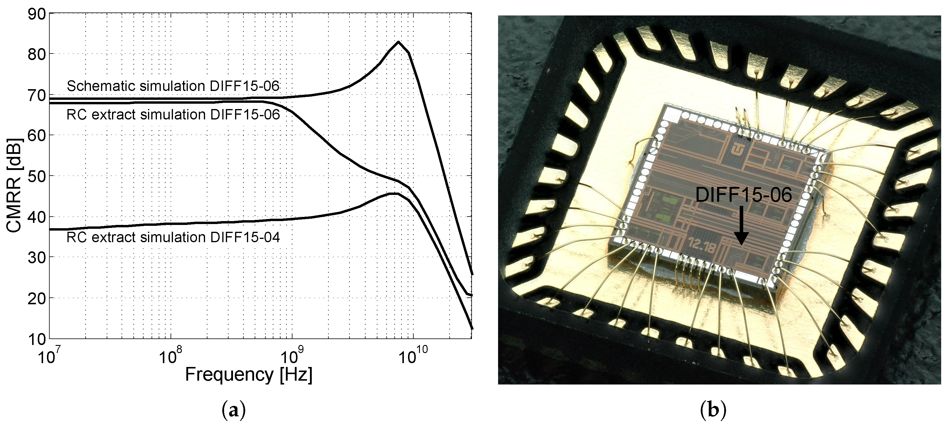
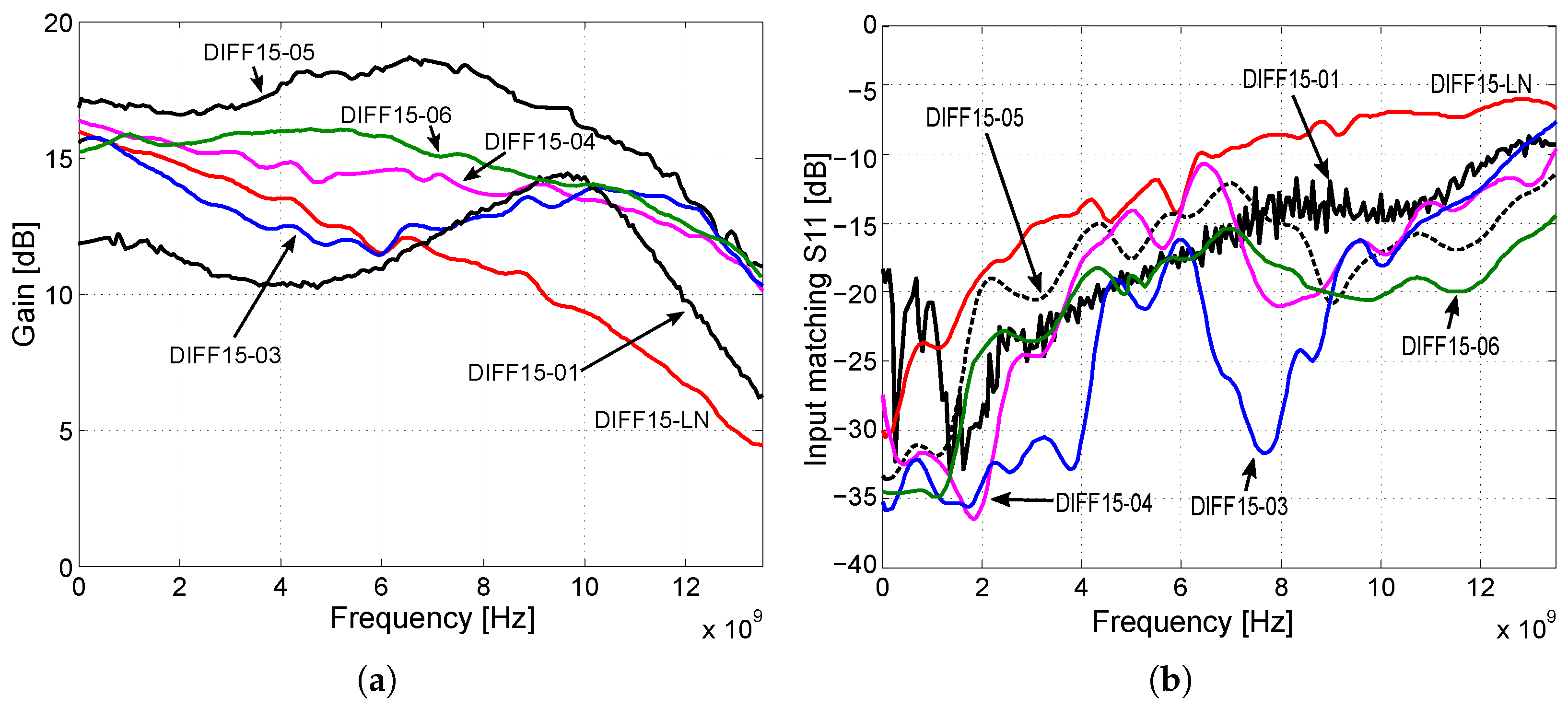
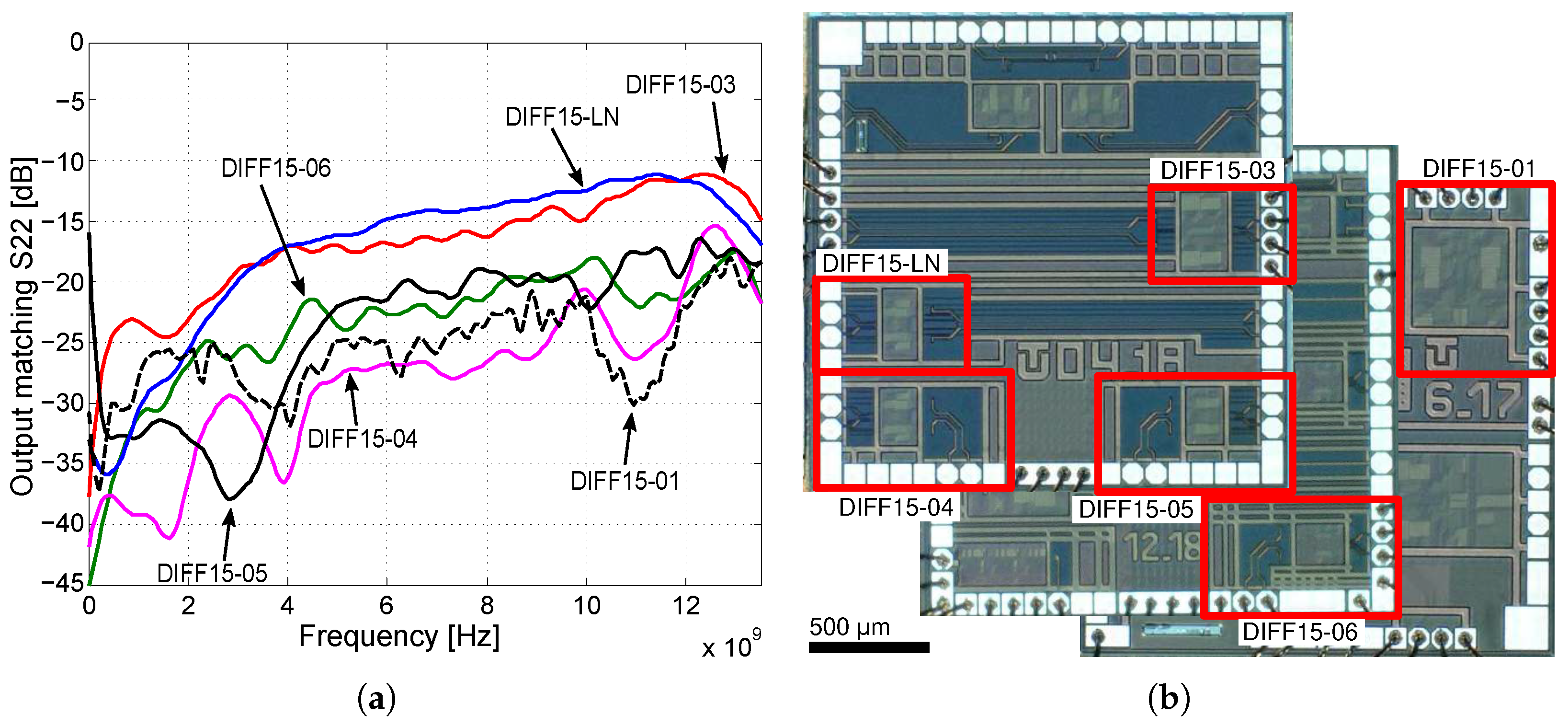
In
Figure 31a,b and
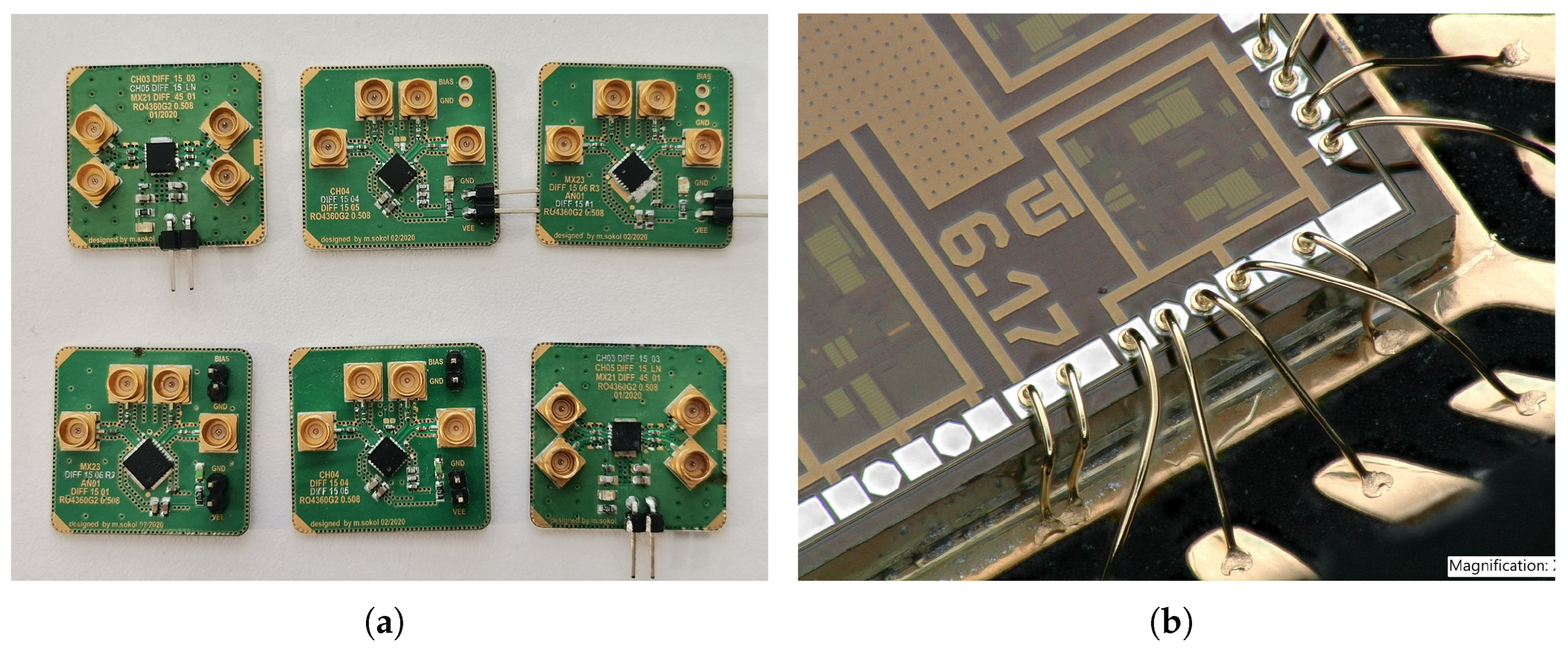
Figure 32a, the measured characteristics of gain, input matching, and output matching are presented to determine the frequency bandwidth. As part of the design of amplifiers, it is important to realize that it is necessary to adjust the resulting voltage gain of all amplifiers to 6 dB higher because on a matched load, the output amplitude of the signal will be a half. This means that for a 15 dB voltage gain, it was necessary to adjust the amplifier core to be 6 dB higher, up to 21 dB. The DIFF15-01, DIFF15-03, and DIFF15-05 amplifiers have the highest bandwidth and show the most significant capacitive peaking. The lowest power consumption comes with DIFF15-06, which has smaller 24 µm NPN232 transistors and a smaller source current; on the other hand, smaller transistors also result in higher noise. If amplifiers are part of other circuits and the output would not come out of the chip, the amplifiers would not need such a large output stage, which, on average, accounts for up to 40% of an amplifier’s total power consumption. The designed amplifier assembled on the evaluation board is shown in
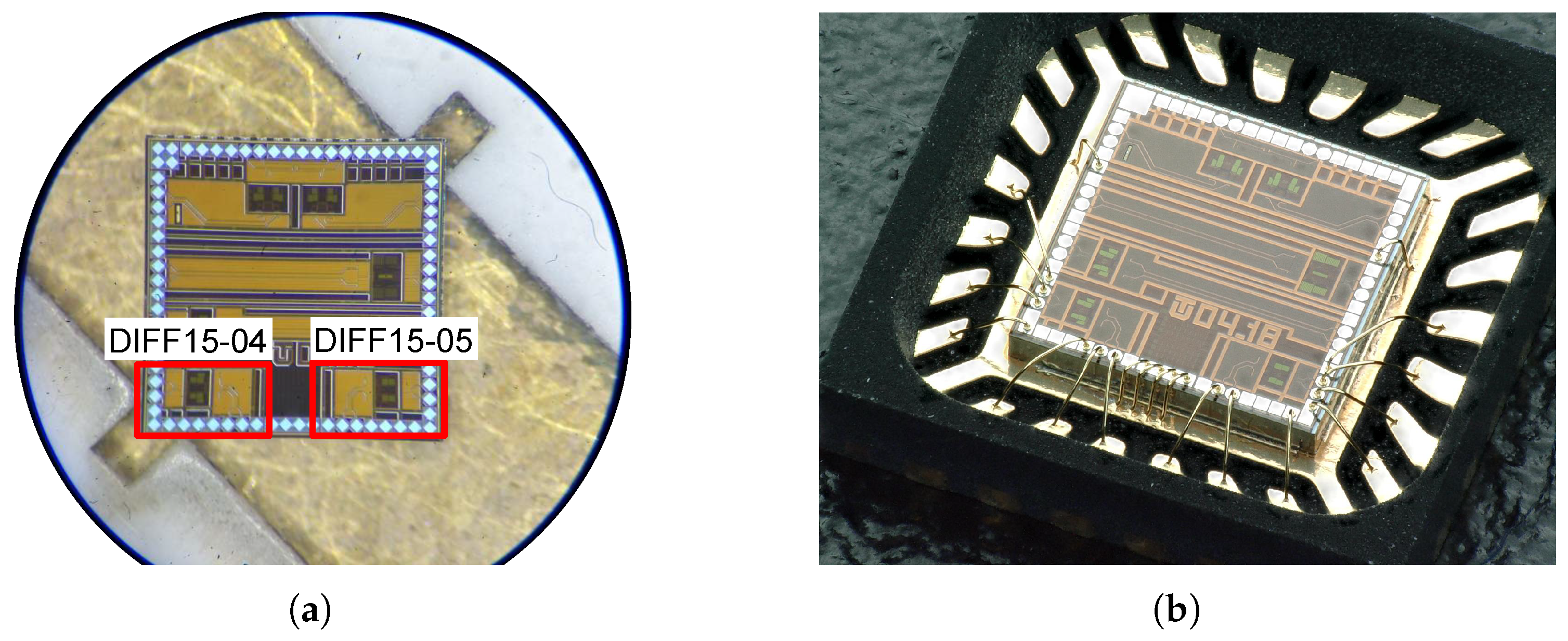
Figure 32a. The dimensions of the fabricated chips are 2 × 2 mm, including other circuit structures which were implemented on the chip dies. A view of the fabricated chips with the amplifiers marked is shown in
Figure 32b.


