
IGBT Overcurrent Capabilities in Resonant Circuits


Abstract
1. Introduction
2. System Construction
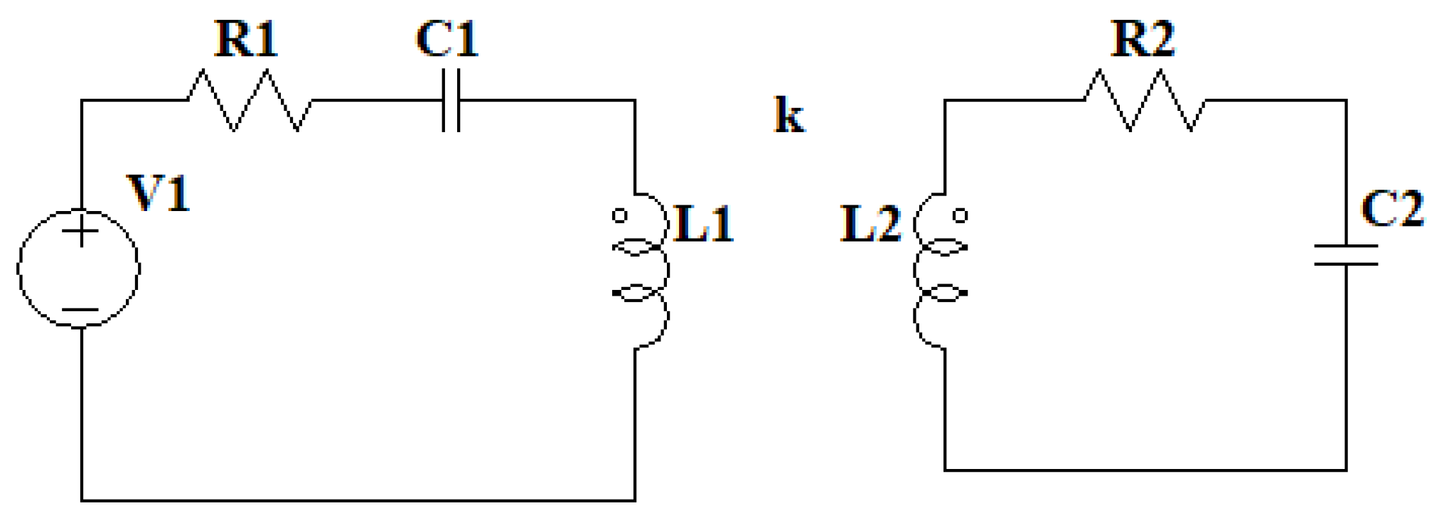
2.1. Resonant Circuits
2.2. H Bridge
2.3. Power Supply
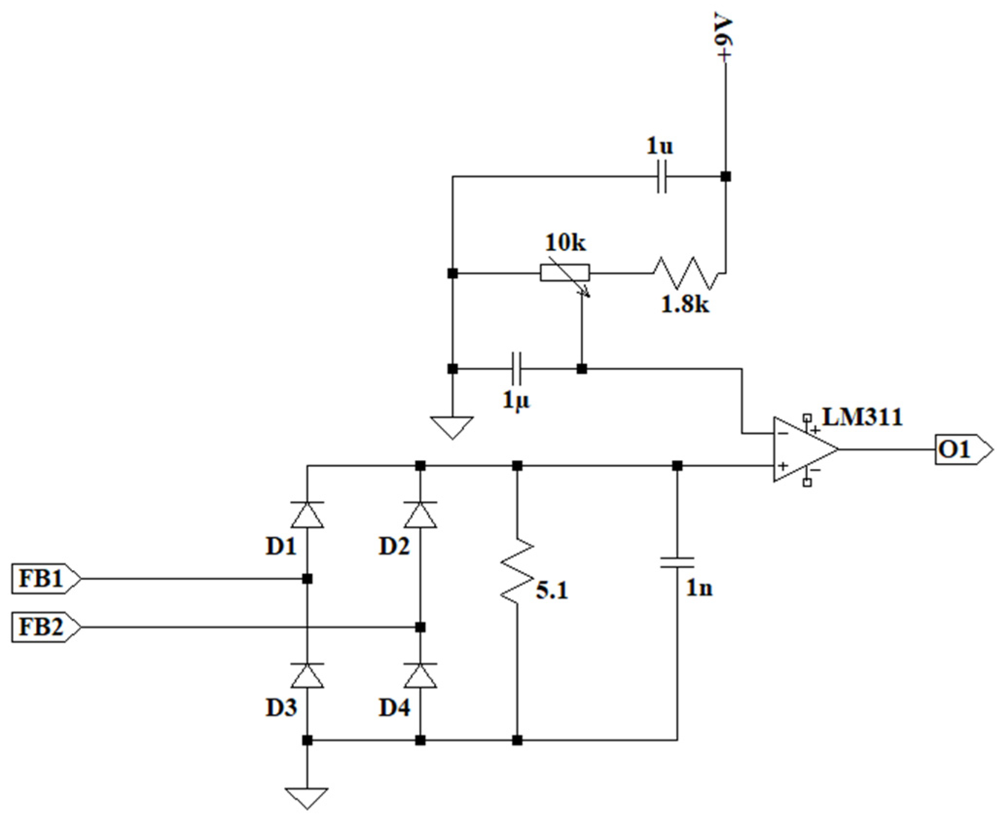
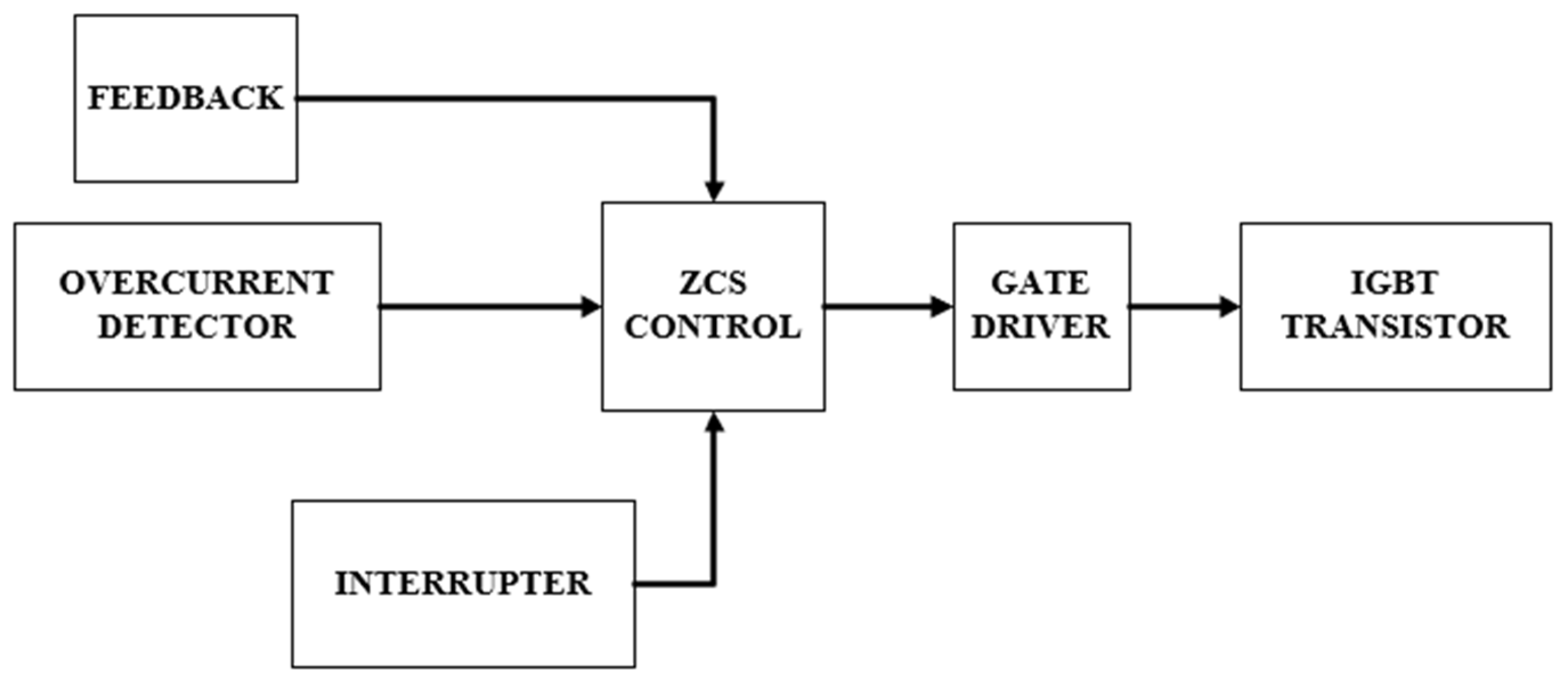
2.4. Feedback and Overcurrent Sensors
2.5. System Control
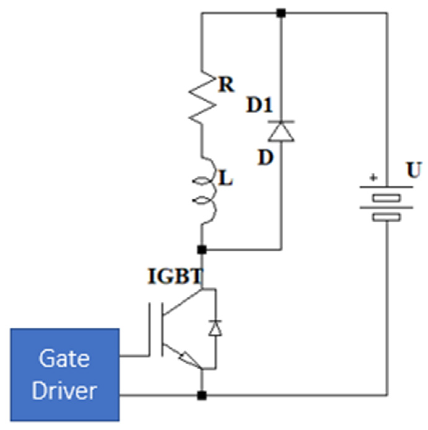
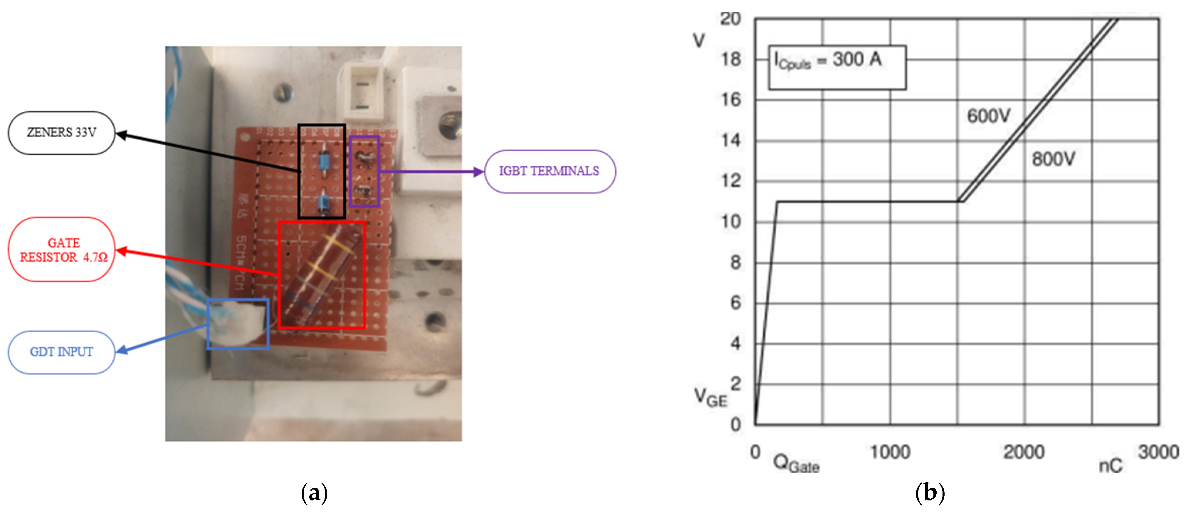
2.6. Drivers
3. Model and Simulation
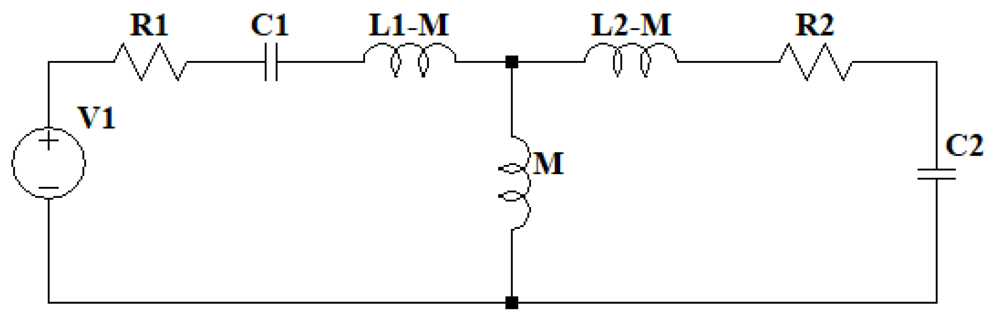
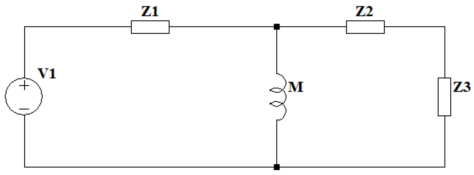
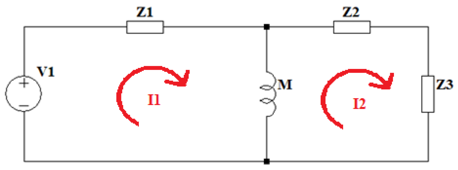
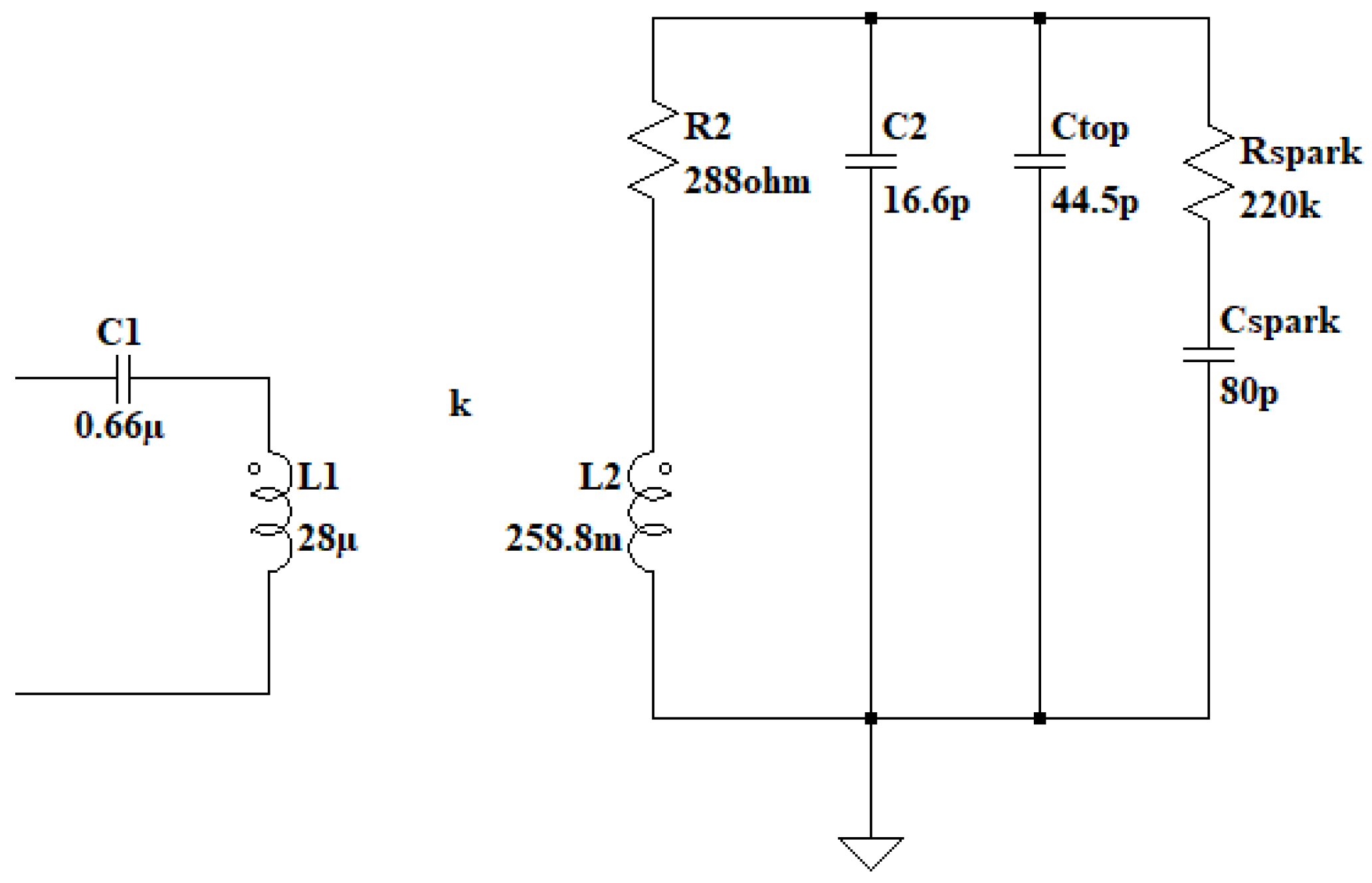
3.1. Resonant Circuit Model
3.2. Output Current
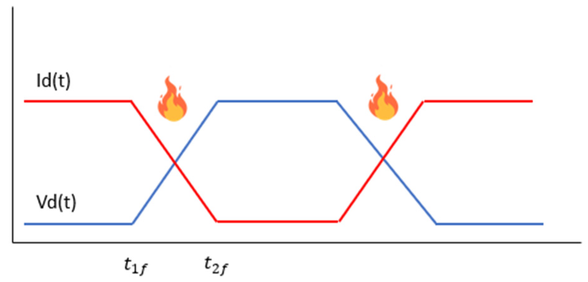
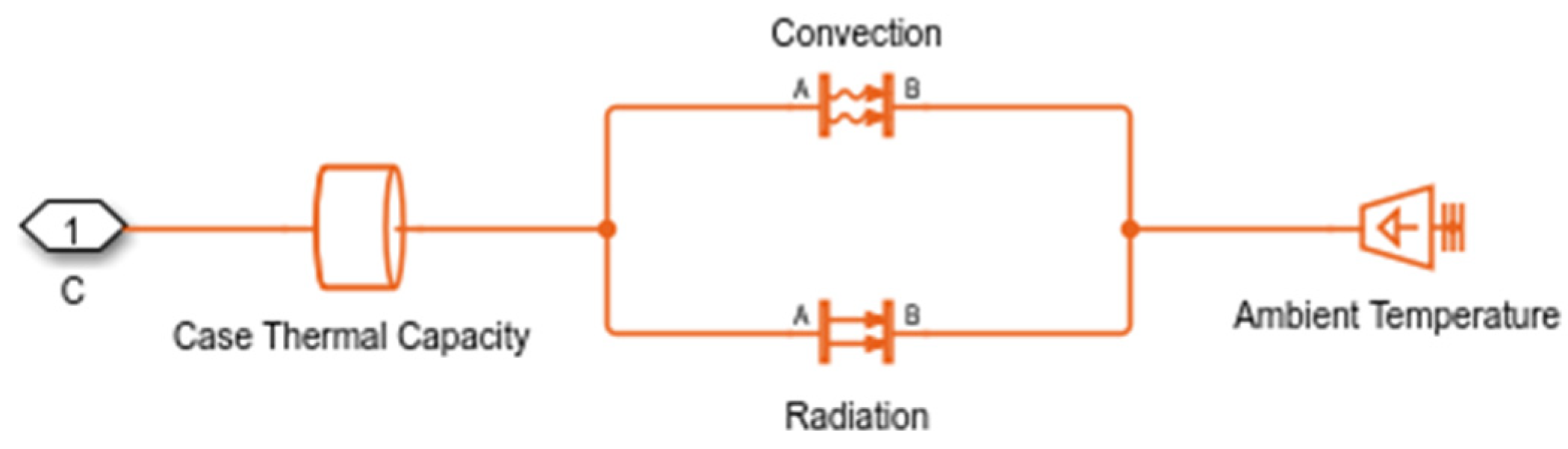
3.3. Model Losses
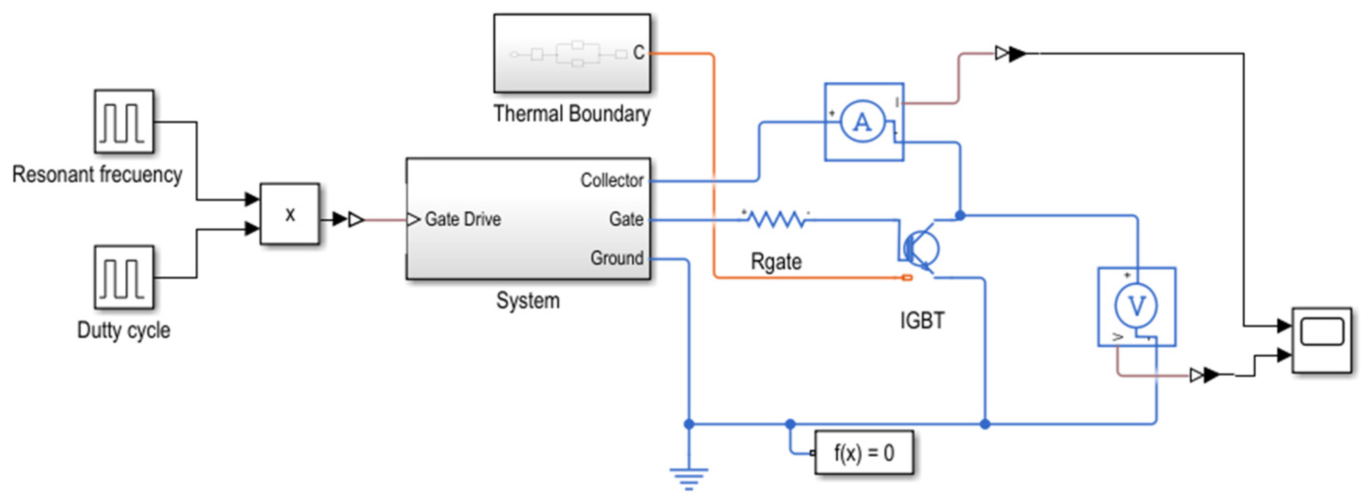
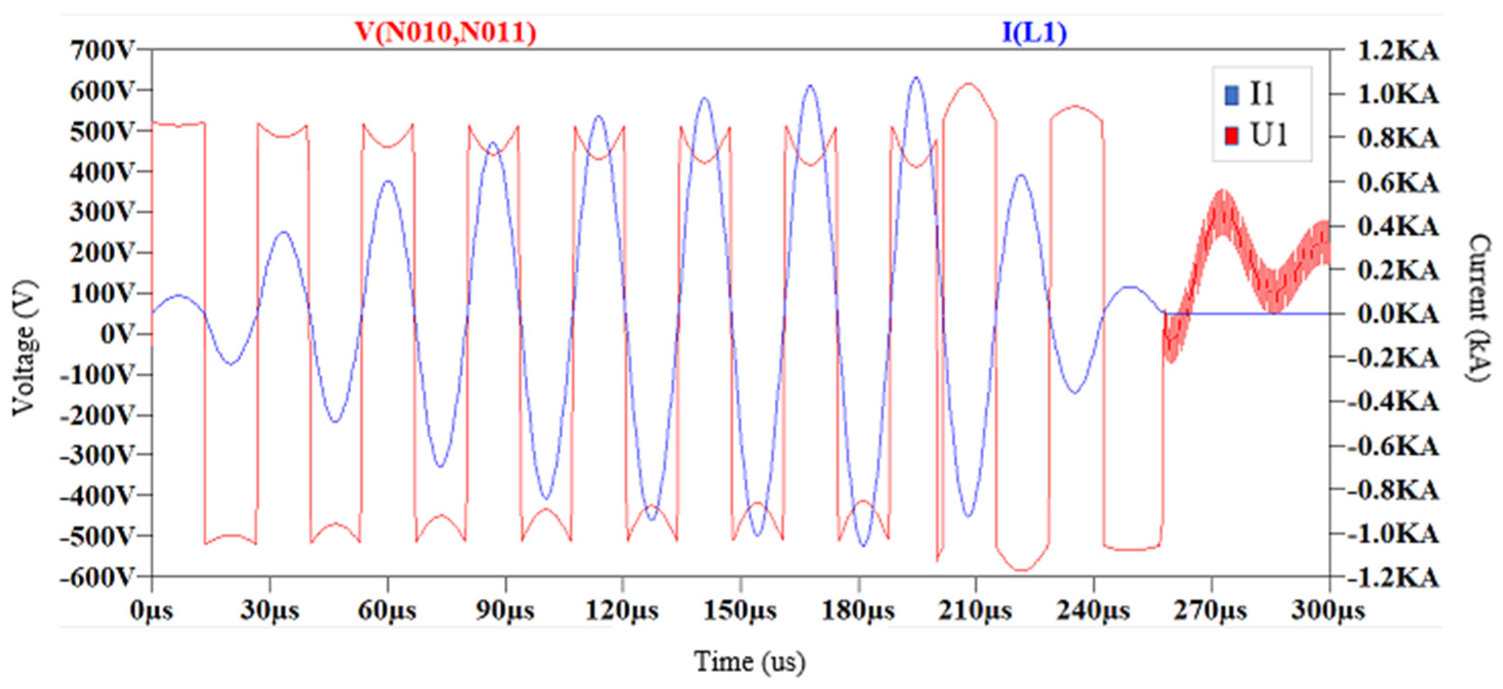
3.4. Spice Simulation
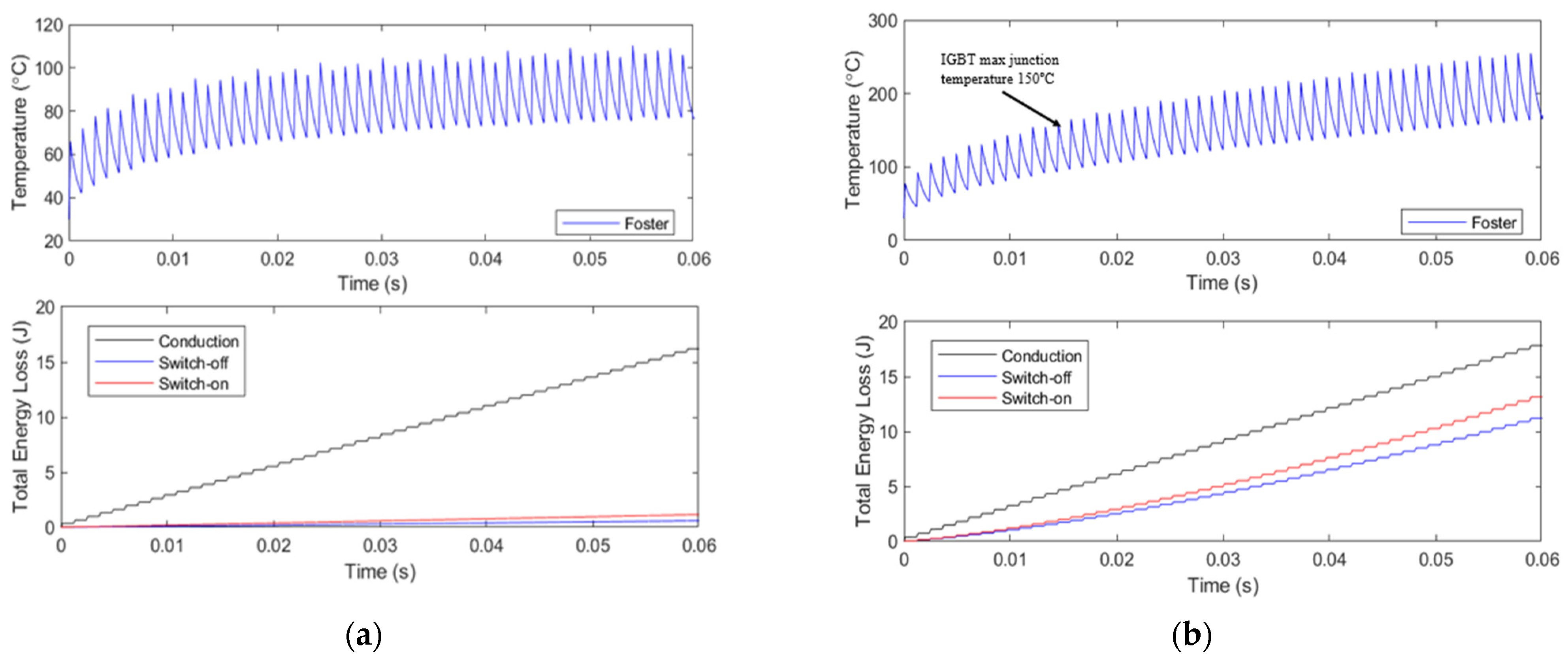
4. Results
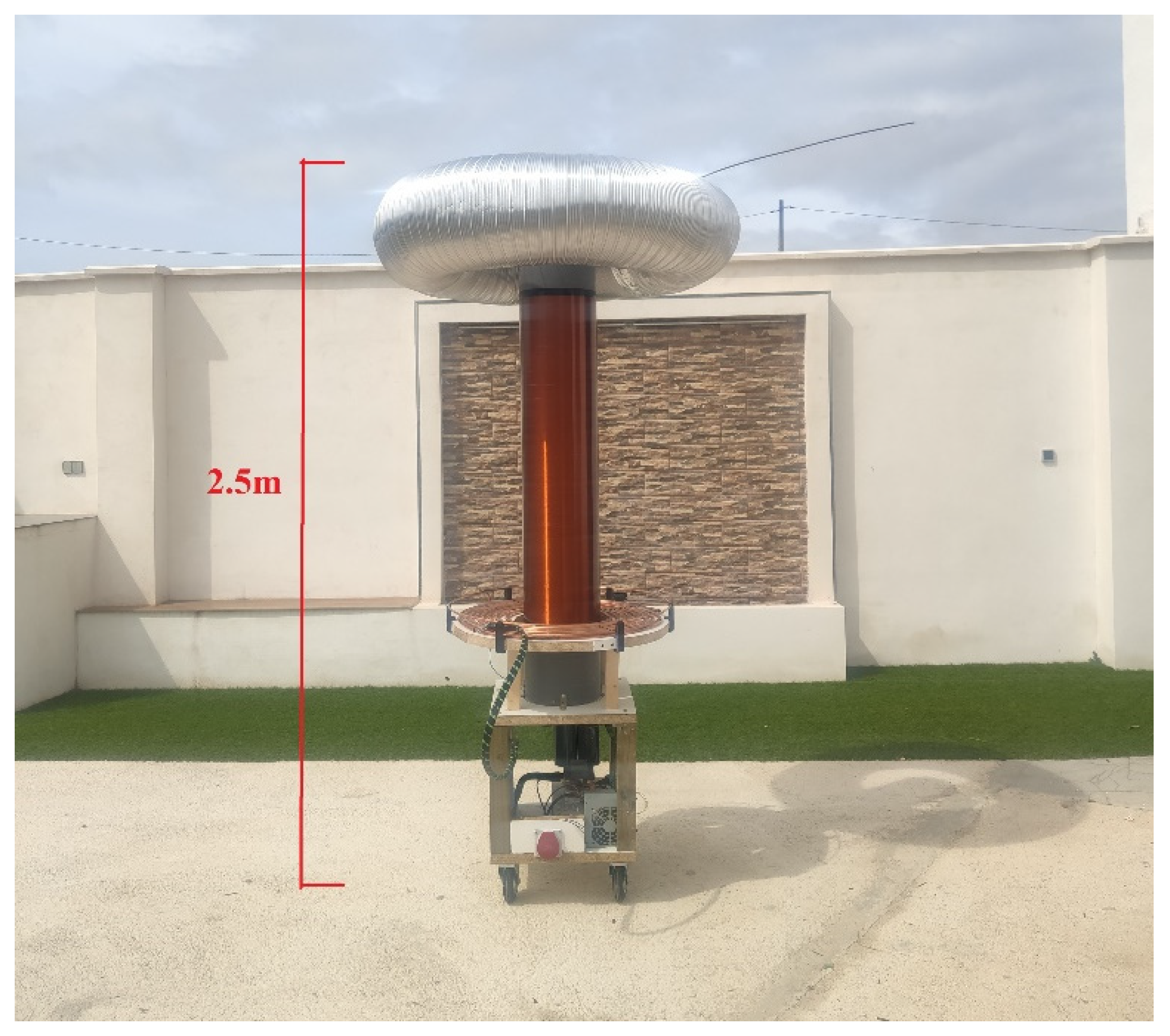
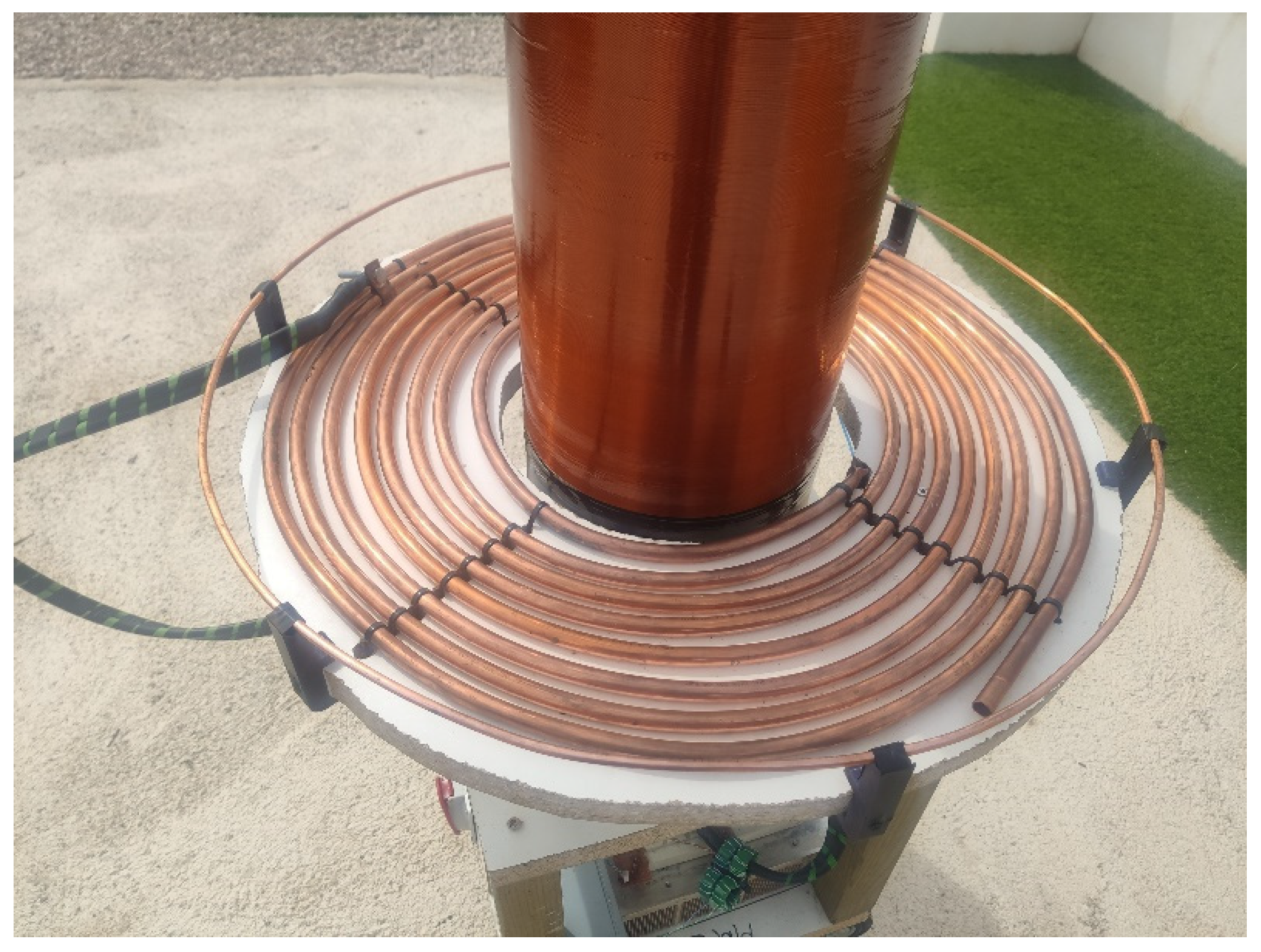
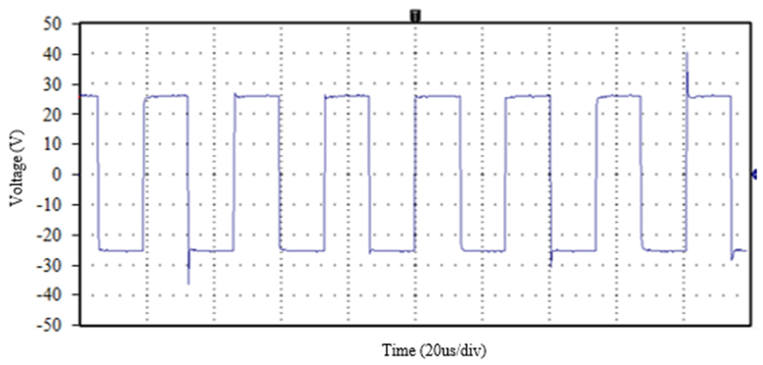
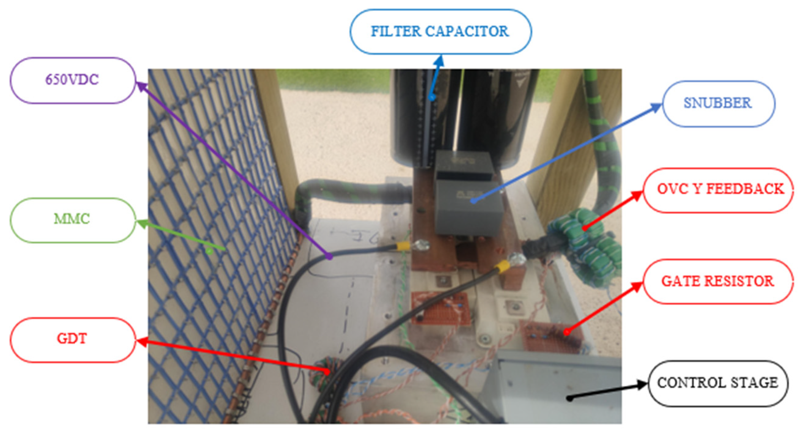
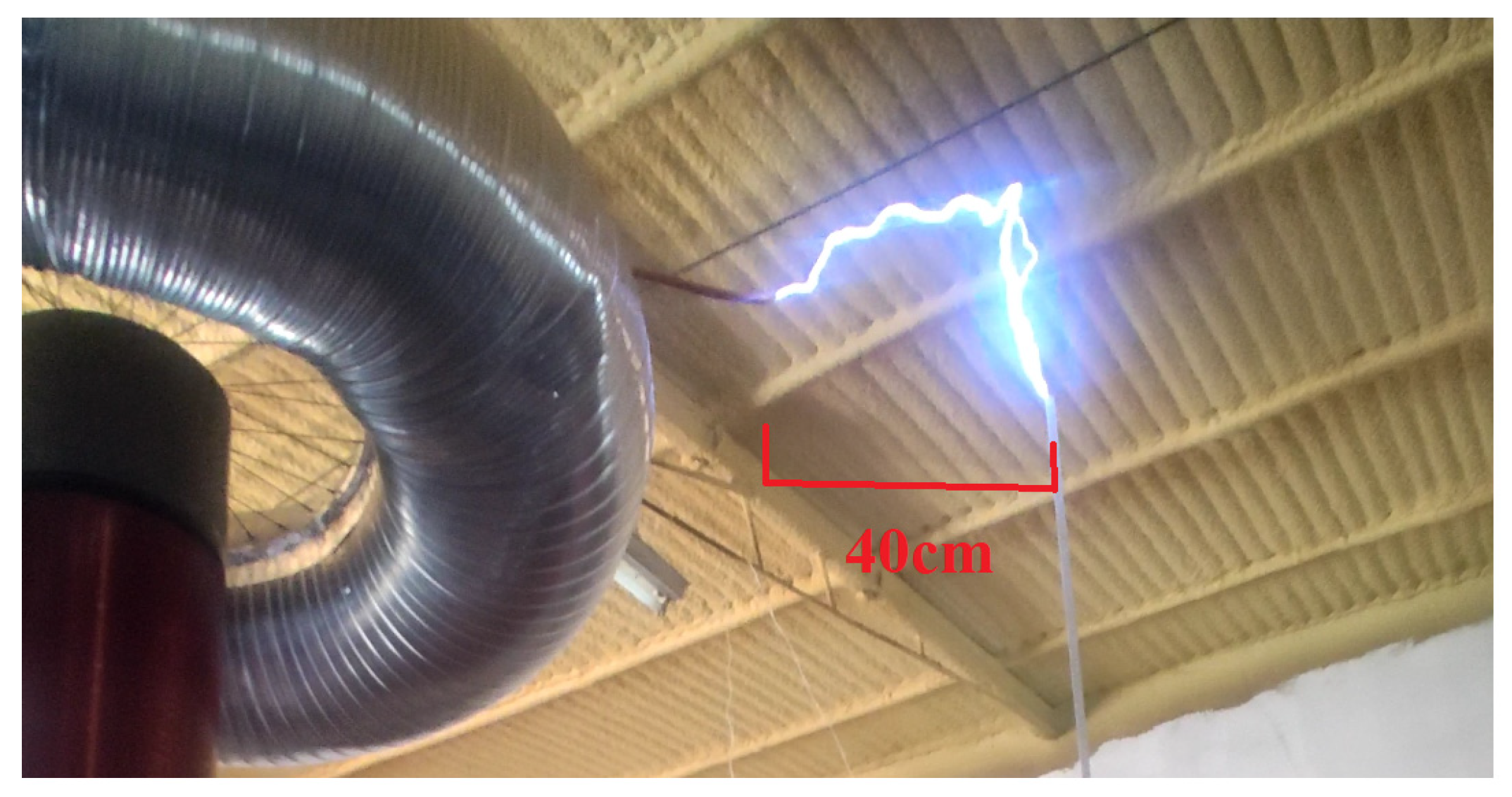
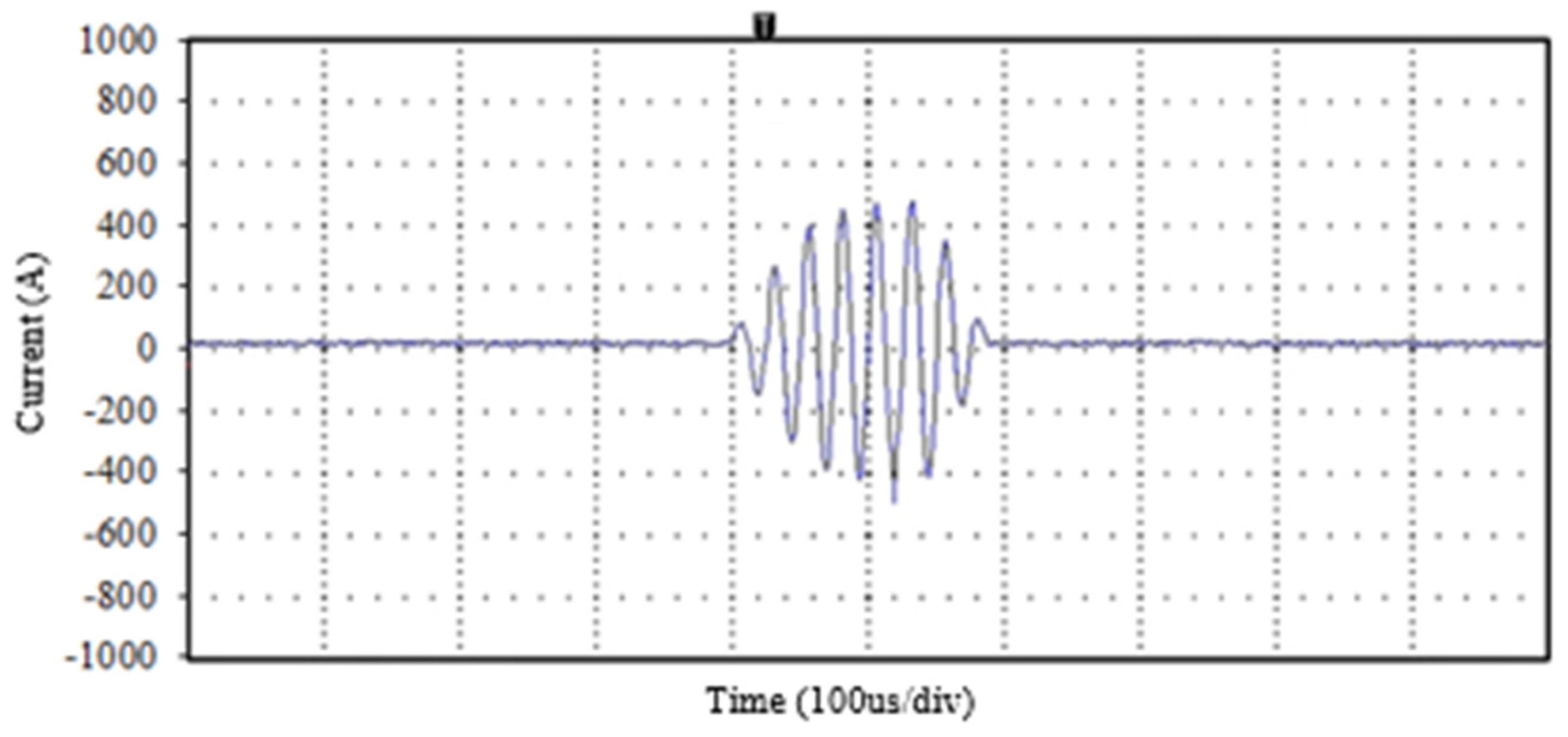
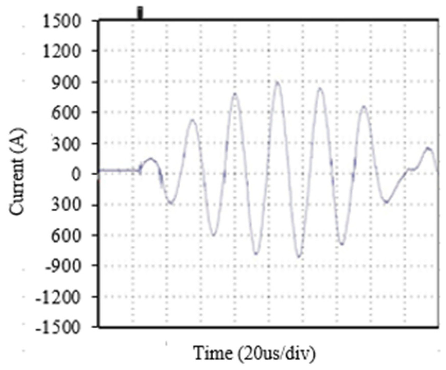
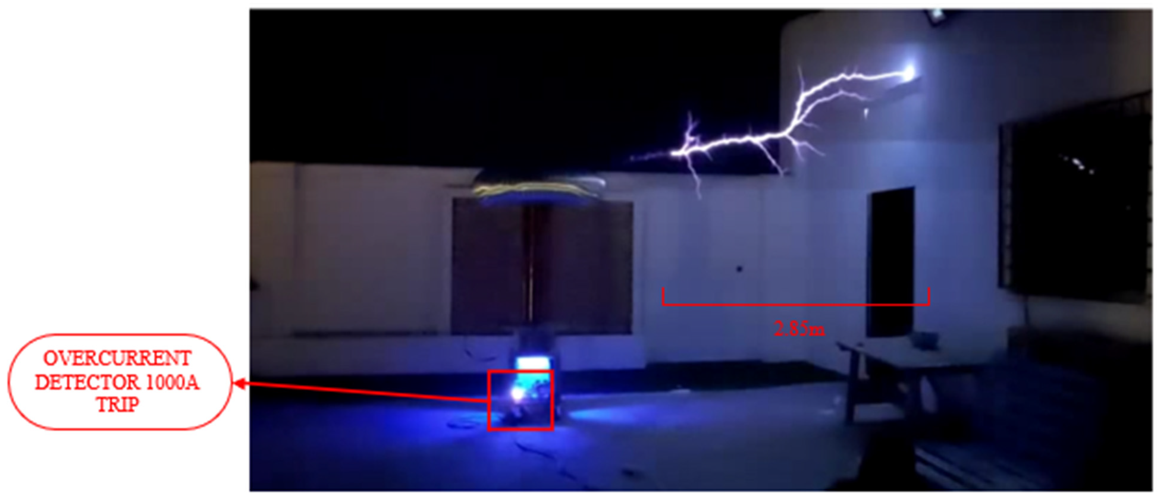
4.1. Prototype Test
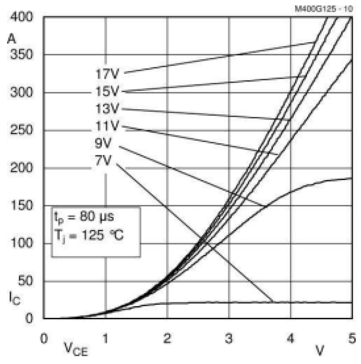
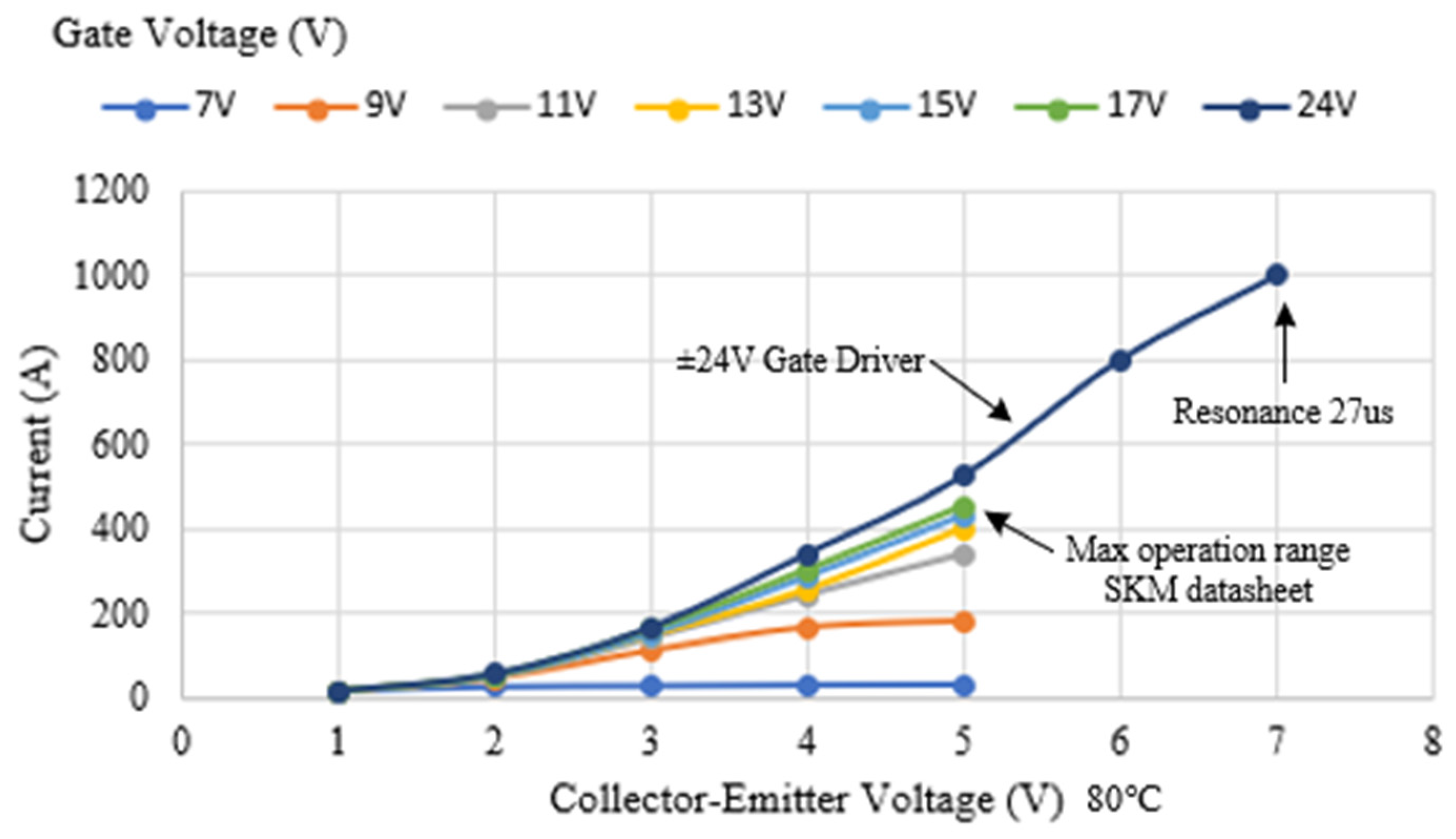
4.2. Operating Currents
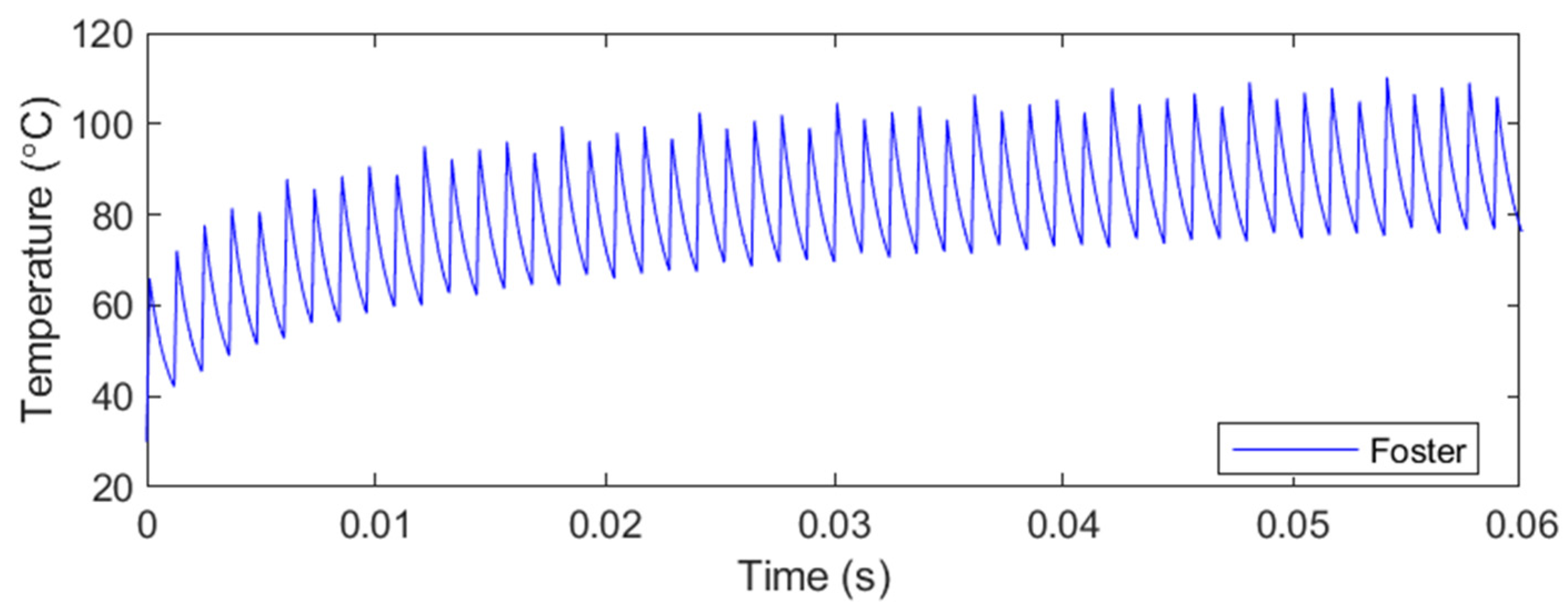
4.3. Final Analysis
5. Conclusions
Author Contributions
Funding
Institutional Review Board Statement
Informed Consent Statement
Data Availability Statement
Conflicts of Interest
References
- Jo, H.-B.; Song, S.-H.; Lee, S.-H.; Ryoo, H.-J. MOSFET Gate Driver Circuit Design for High Repetitive (200 kHz) High Voltage (10 kV) Solid-State Pulsed-Power Modulator. IEEE Trans. Power Electron. 2021, 36, 10461–10469. [Google Scholar] [CrossRef]
- He, N.; Chen, M.; Wu, J.; Zhu, N.; Xu, D. 20-kW Zero-Voltage-Switching SiC-Mosfet Grid Inverter with 300 kHz Switching Frequency. IEEE Trans. Power Electron. 2019, 34, 5175–5190. [Google Scholar] [CrossRef]
- Mori, S.; Aketa, M.; Sakaguchi, T.; Asahara, H.; Nakamura, T.; Kimoto, T. Suppression of Punch-Through Current in 3 kV 4H-SiC Reverse-Blocking MOSFET by Using Highly Doped Drift Layer. IEEE J. Electron Devices Soc. 2018, 6, 449–453. [Google Scholar] [CrossRef]
- Takahashi, Y.; Yoshikawa, K.; Soutome, M.; Fujii, T.; Kirihata, H.; Seki, Y. 2.5 kV-1000 A power pack IGBT (high power flat-packaged NPT type RC-IGBT). IEEE Trans. Electron Devices 1999, 46, 245–250. [Google Scholar] [CrossRef]
- Castagno, S.; Curry, R.D.; Loree, E. Analysis and Comparison of a Fast Turn-On Series IGBT Stack and High-Voltage-Rated Commercial IGBTS. IEEE Trans. Plasma Sci. 2006, 34, 1692–1696. [Google Scholar] [CrossRef]
- Qin, H.; Wang, R.; Xun, Q.; Chen, W.; Xie, S. Switching Time Delay Optimization for “SiC+Si” Hybrid Device in a Phase-Leg Configuration. IEEE Access 2021, 9, 37542–37556. [Google Scholar] [CrossRef]
- Yang, J.; Che, Y.; Ran, L.; Jiang, H. Evaluation of Frequency and Temperature Dependence of Power Losses Difference in Parallel IGBTs. IEEE Access 2020, 8, 104074–104084. [Google Scholar] [CrossRef]
- Singh, A.; Mirafzal, B. An Efficient Grid-Connected Three-Phase Single-Stage Boost Current Source Inverter. IEEE Power Energy Technol. Syst. J. 2019, 6, 142–151. [Google Scholar] [CrossRef]
- Sun, P.; Liu, C.; Lai, J.-S.; Chen, C.-L.; Kees, N. Three-Phase Dual-Buck Inverter with Unified Pulsewidth Modulation. IEEE Trans. Power Electron. 2012, 27, 1159–1167. [Google Scholar] [CrossRef]
- Ranstad, P.; Nee, H.-P. On Dynamic Effects Influencing IGBT Losses in Soft-Switching Converters. IEEE Trans. Power Electron. 2011, 26, 260–271. [Google Scholar] [CrossRef]
- Dulau, L.; Pontarollo, S.; Boimond, A.; Garnier, J.-F.; Giraudo, N.; Terrasse, O. A new gate driver integrated circuit for IGBT devices with advanced protections. IEEE Trans. Power Electron. 2006, 21, 38–44. [Google Scholar] [CrossRef]
- Chen, J.; Zhang, W.J.; Shorten, A.; Yu, J.; Sasaki, M.; Kawashima, T.; Nishio, H.; Ng, W.T. A Smart IGBT Gate Driver IC with Temperature Compensated Collector Current Sensing. IEEE Trans. Power Electron. 2019, 34, 4613–4627. [Google Scholar] [CrossRef]
- Chen, R.; Peng, F.Z. A High-Performance Resonant Gate-Drive Circuit for MOSFETs and IGBTs. IEEE Trans. Power Electron. 2014, 29, 4366–4373. [Google Scholar] [CrossRef]
- Held, M.; Jacob, P.; Nicoletti, G.; Scacco, P.; Poech, M.-H. Fast power cycling test of IGBT modules in traction application. In Proceedings of the Second International Conference on Power Electronics and Drive Systems, Singapore, 26–29 May 1997; Volume 1, pp. 425–430. [Google Scholar] [CrossRef]
- Chen, J.; Deng, E.; Xie, L.; Zhao, Z.; Wu, Y.; Huang, Y. Impact of load pulse duration on failure mechanism of high power IGBT modules under power cycling condition. In Proceedings of the 16th IET International Conference on AC and DC Power Transmission (ACDC 2020), Online, 2–3 July 2020; Volome 2020, pp. 412–417. [Google Scholar] [CrossRef]
- Millan, I.; Puyal, D.; Burdio, J.M.; Lucia, O.; Palacios, D. IGBT selection method for the design of resonant inverters for domestic induction heating. In Proceedings of the 2009 13th European Conference on Power Electronics and Applications, Barcelona, Spain, 8–10 September 2009; pp. 1–7. [Google Scholar]
- Cases, C.; Jordan, J.; Magraner, J.M.; Esteve, V.; Dede, E.; Sanchis, E.; Maset, E.; Ferreres, A.; Ejea, J.; Gumbau, E. Characterization of IGBT devices for use in series resonant inverter for induction heating applications. In Proceedings of the 2009 13th European Conference on Power Electronics and Applications, Barcelona, Spain, 8–10 September 2009; pp. 1–8. [Google Scholar]
- Kleveland, F.; Undeland, T.M.; Langelid, J.K. Increase of output power from IGBTs in high power high frequency resonant load inverters. In Proceedings of the Conference Record of the 2000 IEEE Industry Applications Conference. Thirty-Fifth IAS Annual Meeting and World Conference on Industrial Applications of Electrical Energy (Cat. No.00CH37129), Rome, Italy, 8–12 October 2000; Volome 5, pp. 2909–2914. [Google Scholar] [CrossRef]
- Ghimire, P.; de Vega, A.R.; Beczkowski, S.; Rannestad, B.; Munk-Nielsen, S.; Thogersen, P. Improving Power Converter Reliability: Online Monitoring of High-Power IGBT Modules. IEEE Ind. Electron. Mag. 2014, 8, 40–50. [Google Scholar] [CrossRef]
- Zhang, H.; Yamasaki, H.; Hata, K.; Omura, I.; Takamiya, M. Overcurrent Detection Method by Monitoring Gate Voltage While Periodically Repeating Discharging and Charging of Constant Gate Charge in IGBTs. In Proceedings of the 2022 IEEE 7th Southern Power Electronics Conference (SPEC), Nadi, Fiji, 5–8 December 2022; pp. 1–5. [Google Scholar] [CrossRef]
- Philippou, A.; Jaeger, C.; Laven, J.G.; Baburske, R.; Schulze, H.-J.; Pfirsch, F.; Niedernostheide, F.-J.; Vellei, A.; Itani, H. Critical overcurrent turn-off close to IGBT current saturation. In Proceedings of the 2015 IEEE 27th International Symposium on Power Semiconductor Devices & IC’s (ISPSD), Hong Kong, China, 10–14 May 2015; pp. 113–116. [Google Scholar] [CrossRef]
- Chen, M.; Xu, D.; Zhang, X.; Zhu, N.; Wu, J.; Rajashekara, K. An Improved IGBT Short-Circuit Protection Method with Self-Adaptive Blanking Circuit Based on V CE Measurement. IEEE Trans. Power Electron. 2018, 33, 6126–6136. [Google Scholar] [CrossRef]
- Oh, K.-H.; Kim, Y.C.; Lee, K.H.; Yun, C.M. Investigation of short-circuit failure limited by dynamic-avalanche capability in 600-V punchthrough IGBTs. IEEE Trans. Device Mater. Reliab. 2006, 6, 2–8. [Google Scholar] [CrossRef]
- Xu, Z.; Xu, F.; Wang, F. Junction Temperature Measurement of IGBTs Using Short-Circuit Current as a Temperature-Sensitive Electrical Parameter for Converter Prototype Evaluation. IEEE Trans. Ind. Electron. 2015, 62, 3419–3429. [Google Scholar] [CrossRef]
- Yang, X.; Liu, J.; Wang, B.; Zhang, G. Pulsed Overcurrent Capability of Power Semiconductor Devices in Solid-State Circuit Breakers: SiC MOSFET vs. Si IGBT. In Proceedings of the 2022 IEEE Applied Power Electronics Conference and Exposition (APEC), Houston, TX, USA, 20–24 March 2022; pp. 966–973. [Google Scholar] [CrossRef]
- Costa, E.M.M. Resonance on Coils Excited by Square Waves: Explaining Tesla Transformer. IEEE Trans. Magn. 2010, 46, 1186–1192. [Google Scholar] [CrossRef]
- Krbal, M.; Siuda, P. Design and construction solution of laboratory Tesla coil. In Proceedings of the 2015 16th International Scientific Conference on Electric Power Engineering (EPE), Kouty nad Desnou, Czech Republic, 20–22 May 2015; pp. 311–314. [Google Scholar] [CrossRef]
- Liu, T.; Li, N.; Lv, Z.; Li, C.; Ju, L.; Liu, J. The application of soft-switching and frequency synchronization technologies in electromagnetic heater design. In Proceedings of the 2011 6th IEEE Conference on Industrial Electronics and Applications, Beijing, China, 21–23 June 2011; pp. 1403–1406. [Google Scholar] [CrossRef]
- Jain, A.; Mallik, R.; Catalisano, G.; Abbatelli, L. IGBT over voltage protection scheme in quasi resonant induction heating applications. In Proceedings of the 2015 Annual IEEE India Conference (INDICON), New Delhi, India, 17–20 December 2015; pp. 1–5. [Google Scholar] [CrossRef]
- Panchal, S.; Kulkarni, R.D.; Kumar Raja, M.; Nataraj, J. Design, Simulation and Hardware Implementation of Soft Switching based Induction Heating System. In Proceedings of the 2021 6th International Conference for Convergence in Technology (I2CT), Maharashtra, India, 2–4 April 2021; pp. 1–7. [Google Scholar] [CrossRef]
- Zhao, Y.; Abu Qahouq, J.A. Analysis and Evaluation of Air-core Two-coil Wireless Power Transfer System Configurations. In Proceedings of the 2021 IEEE Applied Power Electronics Conference and Exposition (APEC), Virtual Conference, 14–17 June 2021; pp. 160–163. [Google Scholar] [CrossRef]
- Grandi, G.; Kazimierczuk, M.K.; Massarini, A.; Reggiani, U. Stray capacitances of single-layer solenoid air-core inductors. IEEE Trans. Ind. Appl. 1999, 35, 1162–1168. [Google Scholar] [CrossRef]
- Jain, P.K.; Espinoza, J.R.; Dewan, S.B. Self-started voltage-source series-resonant converter for high power induction heating and melting applications. In Proceedings of the IAS ’97. Conference Record of the 1997 IEEE Industry Applications Conference Thirty-Second IAS Annual Meeting, New Orleans, LA, USA, 5–9 October 1997; Volome 2, pp. 1653–1660. [Google Scholar] [CrossRef]
- Uma, G.; Senthilkumar, R. Design of resonant soft switching converter. In Proceedings of the Communication and Energy Conservation 2009 International Conference on Control, Automation, Perundurai, Erode, India, 4–6 June 2009; pp. 1–6. [Google Scholar]
- Hu, S.-W.; Zhu, Y.-J.; Duan, Y.-Y. An impact analysis of gate resistance on static and dynamic dissipation of IGBT modules. In Proceedings of the 2011 International Conference on Electronics, Communications and Control (ICECC), Ningbo, China, 9–11 September 2011; pp. 715–718. [Google Scholar] [CrossRef]
- Hadizade, A.; Nasab, J.N.; Aghaei, M.; Kaboli, S. Investigations on equivalent circuit models of high frequency transformers. In Proceedings of the 2018 9th Annual Power Electronics, Drives Systems and Technologies Conference (PEDSTC), Tehran, Iran, 13–15 February 2018; pp. 475–480. [Google Scholar] [CrossRef]
- Bhowmick, D.; Manna, M.; Chowdhury, S.K. Estimation of equivalent circuit parameters of transformer and induction motor using PSO. In Proceedings of the 2016 IEEE International Conference on Power Electronics, Drives and Energy Systems (PEDES), Trivandrum, India, 14–17 December 2016; pp. 1–6. [Google Scholar] [CrossRef]
- Alavi, O.; Abdollah, M.; Hooshmand Viki, A. Assessment of thermal network models for estimating IGBT junction temperature of a buck converter. In Proceedings of the 2017 8th Power Electronics, Drive Systems & Technologies Conference (PEDSTC), Mashhad, Iran, 14–16 February 2017; pp. 102–107. [Google Scholar] [CrossRef]


| Parameter | Value |
|---|---|
Disclaimer/Publisher’s Note: The statements, opinions and data contained in all publications are solely those of the individual author(s) and contributor(s) and not of MDPI and/or the editor(s). MDPI and/or the editor(s) disclaim responsibility for any injury to people or property resulting from any ideas, methods, instructions or products referred to in the content. |
© 2024 by the authors. Licensee MDPI, Basel, Switzerland. This article is an open access article distributed under the terms and conditions of the Creative Commons Attribution (CC BY) license (https://creativecommons.org/licenses/by/4.0/).
Share and Cite
Al-Hadithi, B.M.; Jimenez, M. IGBT Overcurrent Capabilities in Resonant Circuits. Sensors 2024, 24, 7631. https://doi.org/10.3390/s24237631
Al-Hadithi BM, Jimenez M. IGBT Overcurrent Capabilities in Resonant Circuits. Sensors. 2024; 24(23):7631. https://doi.org/10.3390/s24237631
Chicago/Turabian StyleAl-Hadithi, Basil Mohammed, and Miguel Jimenez. 2024. "IGBT Overcurrent Capabilities in Resonant Circuits" Sensors 24, no. 23: 7631. https://doi.org/10.3390/s24237631
APA StyleAl-Hadithi, B. M., & Jimenez, M. (2024). IGBT Overcurrent Capabilities in Resonant Circuits. Sensors, 24(23), 7631. https://doi.org/10.3390/s24237631