Abstract
In this paper, a novel current-mode shadow filter employing current-controlled current conveyors (CCCIIs) with controlled current gains is presented. The CCCII-based current-mode shadow filters are resistorless and can offer a number of advantages such as circuit simplicity and electronic tuning capability. The proposed shadow filters offer five filtering functions, i.e., low-pass, high-pass, band-pass, band-stop, and all-pass functions, in the same topology. Furthermore, no component matching condition is required to realize all the transfer functions. The natural frequency and quality factor adjustment is possible by using the CCCII current gains without the need to use external amplifiers, all capacitors are grounded, and the filter terminals offer low-input and high-output impedance. To verify the functionality and feasibility of the new topologies, the proposed circuits were simulated using SPICE and the transistor model process parameters NR100N (NPN) and PR100N (PNP) from AT&T’s bipolar arrays ALA400-CBIC-R. The simulation results are consistent with the theory. The CCCII experimental setup was designed using commercially available 2N3904 (NPN) and 2N3906 (PNP) transistors with a supply voltage of ±2.5 V. The measurement results confirm the performance of the designed filters.
1. Introduction
Over the last decade, second-generation current conveyors (CCIIs) have been used to realize current-mode analog circuits. This is because CCII-based circuits offer better signal bandwidth, higher linearity, circuit simplicity, and wider dynamic range performances compared with the operational amplifiers (op-amps)-based circuits [1,2]. In addition, a CCII is simpler to implement compared to the op-amp structure.
Usually, a conventional CCII has three terminals (x-, y-, and z-terminal) [3]. Its electrical symbol is shown in Figure 1, while its terminal characteristics in ideal case are given by Equation (1).
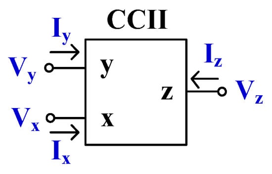
Figure 1.
Electrical symbol of CCII.
It can be noted that the y-terminal is a voltage input that has a high impedance level (ideally infinity), the x-terminal is a voltage signal output and also a current signal input, with low impedance level (ideally zero), and the z-terminal is a current output with a high impedance level (ideally infinity). In practice, the parasitic resistance at the x-terminal (Rx) of the CCII can be controlled by its bias current, which can be used as a design parameter. Such a device is called a current-controlled current conveyor (CCCII) [4]. Circuits based on CCCII can thus reduce the number of passive resistors and offer the possibility of electronic control.
It should be noted that in the ideal case is Vx = Vy for CCII and Vx = IxRx + Vy for CCCII, while Iz = Ix for both circuits. Note that the voltage and current gain in these formulas is equal to one. To increase the functionality, the CCCII with controlled current gain has also been proposed [5]. This device offers an adjustable current gain between the z- and x-terminals, which can be used as a design parameter for such applications as filters and oscillators. The CCII/CCCII can be realized using bipolar junction transistor (BJT) technology [5] or complementary metal oxide semiconductor (CMOS) technology [6,7]. In this work, a CCCII with controlled current gain is used to realize current-mode shadow filters.
The shadow filter was first introduced in [8]. The concept of the conventional shadow filter is to use an external amplifier to adjust the natural frequency and the quality factor of the second-order filters without changing the value of parameters such as capacitances and resistances of the original topology. However, the shadow filter in [8] does not provide independent control of the natural frequency and the quality factor. To obtain independent control of the above-mentioned parameters, the shadow filter was further developed, and two new systems were proposed [9]. The first system in [9] consists of a second-order filter and an amplifier. The LP and BP outputs are summed and amplified by the amplifier, and the output signal of the amplifier is summed with the input signal. Thus, the quality factor can be controlled by an external amplifier without changing the natural frequency. The second system in [9] was further developed by adding another amplifier to the first system. Thus, the second system in [9] consists of a second-order filter and two external amplifiers. The first amplifier is used to amplify the BP output, while the second one is used to amplify the LP output, and the output signals of the two amplifiers are summed with the input signal. Consequently, the quality factor can be modified by the first external amplifier, while the natural frequency can be modified by the second one. In this work, the two systems of shadow filters in [9] will be designed using CCCII with controlled current gain as active elements. It will be shown that the function of external amplifiers can be obtained using the current gains of CCCIIs.
Many shadow filters (also known as frequency-agile filters) have been introduced [10,11,12,13,14,15,16,17,18,19,20,21,22,23,24,25,26,27,28,29,30,31,32,33,34]. These filters can be used for various radio applications and sensor networks including environmental monitoring, vital signs monitoring, and military applications. Considering the operating mode of these filters, they can be divided into three operating modes: voltage-mode [10,11,12,13,14,15,16,17,18,19,20,21,22], current-mode [23,24,25,26,27,28,29,30,31], and mixed-mode (or multi-mode) [32,33,34].
Considering the active devices used to realize the voltage-mode shadow filters in [10,11,12,13,14,15,16,17,18,19,20,21,22], the circuit in [10] uses operational transresistance amplifiers (OTRA), the circuits in [11,12,13] use current-feedback operational amplifiers (CFOA), the circuits in [14,16,17,18] use voltage differencing transconductance amplifiers (VDTA), the circuit in [15] uses voltage differencing differential difference amplifiers (VDDDA), the circuit in [19] uses voltage differencing gain amplifiers (VDGA), while the circuit in [21] uses operational transconductance amplifiers (OTA), and the circuits in [22] use differential difference transconductance amplifiers (DDTA). The shadow filters in [15,16,17,18,19,21,22] offer an electronic tuning capability, but only the filter in [15] offers five filtering functions, namely low-pass (LP), high-pass (HP), band-pass (BP), band-stop (BS), and all-pass (AP). However, the voltage-mode filter in [15] does not provide low-output impedance, which is required for voltage-mode circuits.
This work is focused on the current-mode shadow filter that offers low-input and high-output impedances, which is required for current-mode circuits. With respect to the current-mode shadow filters in [23,24,25,26,27,28,29,30,31], the circuits in [23,24,25,26,27] use current difference transconductance amplifier (CDTA), the circuit in [28] uses operational floating current conveyor (OFCC), the circuit in [29] uses current backwards trans-conductance amplifier (CBTA), while the circuit in [30] uses current controlled current differencing cascadedtransconductance amplifier (CC-CDCTA), and the circuit in [31] uses current conveyor cascaded transconductance amplifier (CCCTA). The shadow filters in [23,24,25,26,27,29,30,31] offer an electronic tuning capability, but only the shadow filter in [31] can offer low-pass, high-pass, band-pass, band-stop, and all-pass filtering functions in one system. The circuit in [31] employs one CCCTA, one EX-CCCTA, and two capacitors. Although the circuit is based on a small number of active blocks, the structure of active blocks is rather complex.
With respect to the mixed-mode shadow filters in [32,33,34], the circuit in [33,34] can realize low-pass, high-pass, band-pass, band-stop, and all-pass filtering functions in the same topology. However, when the mixed-mode circuit in [33] operates in current-mode, the input matching condition, namely Iin = Iin1 = Iin2, is required. This means that the circuit requires additional circuits to produce multiple copies of a single input signal. The filter in [33] employs two FD-CCCTAs (fully differential current conveyor cascaded transconductance amplifier), three capacitors, and two MOS resistors, while the filter in [34] employs two DDCCCTAs (differential current conveyor cascaded transconductance amplifiers), two capacitors, and one MOS resistor. However, the active block structures used in these filters [34,35] suffer from a relatively high complexity.
This paper presents current-mode shadow filters using CCCIIs with controlled current gain as active elements. The circuits employ three CCCIIs and two grounded capacitors. This work shows that the current gains of the used CCCIIs can perform the role of external amplifiers to adjust the natural frequency and quality factor of the proposed universal filters without the need to modify their internal parameters. The proposed current-mode shadow filters offer low-pass, high-pass, band-pass, band-stop, and all-pass filtering functions in the same topology with low complexity. The natural frequency and the quality factor can be adjusted by the current gains of CCCIIs and can be electronically controlled. The proposed current-mode filters offer low-input and high-output impedances, which is desirable in current-mode circuits. The paper is organized as follows: Section 2 describes the structure of the CCCII with controlled current gain, the proposed current-mode shadow filters and the nonideality analysis. The simulation results of the CCCII with controlled current gain and the shadow filter are shown in Section 3. Section 4 presents the experimental results of the proposed filters and Section 5 concludes the paper.
2. Proposed Circuit
2.1. CCCII with Controlled Current Gain
The electrical symbol of the CCCII with controlled current gain and multiple current outputs is shown in Figure 2. In the ideal case, this element can be described by the following matrix equation:
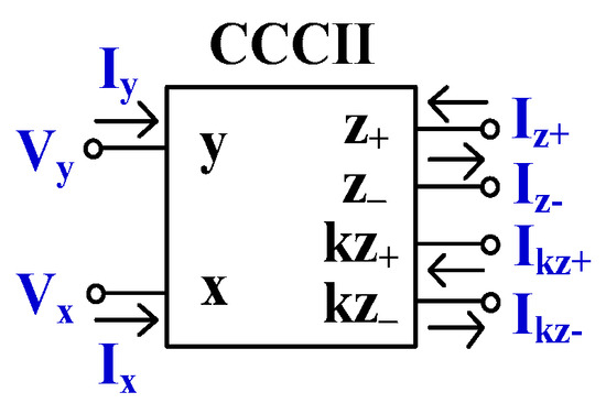
Figure 2.
Electrical symbol of the CCCII with controlled current gain.
The CCCII with controlled current gain can be implemented using both BJT [5,6,7] as well as CMOS [6,7] technologies. This paper proposes a simple BJT implementation shown in Figure 3. The main circuit consists of the translinear loop (Q1-Q4) and the positive and negative current mirrors with adjustable gain (Q22-Q25, Q26-Q29). Assume that transistors Q1 to Q4 of a translinear loop are identical and are biased by the current Iset. The parasitic resistance at x-terminal is given by [4]:
where VT is the thermal voltage (~26 mV at 27 °C) and Iset is the bias current. Note that Rx can be controlled by Iset.
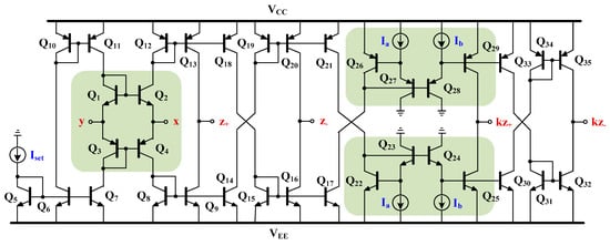
Figure 3.
BJT implementation of the CCCII with controlled current gain.
Assuming further that transistors Q22 to Q25 of positive current mirrors and transistors Q26 to Q29 of the negative current mirrors are identical, the current gain k of the CCCII in Figure 3 is given by [5]:
It should be noted that the current gain k can be linearly controlled. Moreover, it is independent of temperature variation.
2.2. Proposed Current-Mode Shadow Filter
Figure 4a shows the block diagram of the current-mode shadow filter, which consists of a second-order filter (2nd-order filter) that provides three filtering functions i.e., LP, HP, and BP filters, and the amplifier (A) [9]. The outputs of the LP and HP filters are further summed and amplified by the amplifier A, and the output signal of the amplifier is then summed with the input signal. Figure 4b shows the first proposed current-mode shadow filter based on the translinear current conveyors (CCCIIs) with controlled current gains, which is realized based on the block diagram in Figure 4a. The CCCII1 to CCCII3, C1, and C2 form a second-order filter that provides three outputs of, LP, HP, and BP filters. This is based on two integrator loops, of which CCCII1 and C1 create the first integrator, and CCCII2, and C2 create the second. The current gains of CCCII2 (k2) and CCCII3 (k3) act as an external amplifier (i.e., k2 = k3 = k = A). The outputs of the LP and HP filters are amplified by k2 and k3, respectively, and are next fed to the input node of the filter. Thanks to the multiple-output CCCII, the BS filter (IBS) can be obtained by summing the outputs of the LP and HP filters.
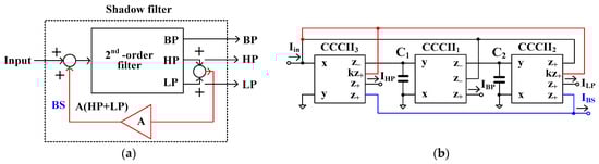
Figure 4.
First current-mode shadow filter: (a) block diagram, (b) first proposed current-mode shadow filter using CCCIIs.
It should be noted that the input current Iin is applied to the x-terminal of CCCII which provides a low impedance level, while the output currents ILP, IHP, IBP, and IBS are supplied from the z-terminals of the CCCII which provides a high impedance level. The circuit uses two grounded capacitors and no passive resistors, which reduces the chip area when it is realized in integrated form.
Using nodal analysis and (2), the output currents of the LP (), HP (), BP (), and BS () filters in Figure 4b can be respectively expressed as
By combining the currents and , the output current of the AP filter () can be obtained as
where and are, respectively, the parasitic resistances of CCCII1 and CCCII2, while and are, respectively, the current gains of CCCII2 and CCCII3.
Assuming (, the natural frequency () and the quality factor () can be respectively given by
It should be noted that the parameter can be electronically controlled by and via and (i.e., ) and the parameter can be electronically controlled via ( = = ).
From (5), (6), (8), and (9), it can be seen that when the parameter is varied by , the passband gains of the LP, HP, BS, and AP filters change. Namely, increasing the value will decrease the passband gains of these filters, except the passband gain of the BP filter, which will be constant.
It should be noted that the shadow filter in Figure 4 uses one external amplifier to modify only the quality factor. Figure 5a shows the block diagram for the second current-mode shadow filter which consists of a 2nd order filter and two amplifiers (A1 and A2) [9]. The output signals BP and LP are amplified, respectively, by A1 and A2, and summed with the input signal. Thus, the quality factor and the natural frequency can be independently controlled using the amplifiers A1 and A2.
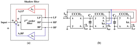
Figure 5.
Second current-mode shadow filter: (a) block diagram, (b) second proposed current-mode shadow filter using CCCIIs.
Figure 5b shows the proposed second realization of the current-mode shadow filter using CCCIIs with controlled current gains, which realizes the block diagram in Figure 5a. The CCCII1 to CCCII3, C1, and C2 form a second-order filter that provides three outputs of the LP, HP, and BP filters, which are similar to the ones in Figure 4b. Compared with Figure 5a, the gain A1 is realized by k1 of CCCII1 and A2 is realized by k2 of CCCII2. The output of the BP filter is amplified by k1 and the output of the LP filter is amplified by k2. The amplified output signals of the BP and LP filters are applied to the input node of the filter.
Using nodal analysis and (2), the output currents of the LP (), HP (), BP (), and BS () filters of Figure 5b can be respectively expressed as
From and , the output current of the BS filter () can be obtained as
From , and , the output current of the AP filter () can be obtained as
The natural frequency () and the quality factor () of the filters are given by
As can be seen, the parameter can be controlled by k2 (A2) in the range of 0 < k2 < 1 and the parameter can be controlled by k1 (A1) in the range of 0 < k1 < 1. Thus, the parameters and can be independently controlled. It could be noted that adjusting the parameter by k2 will affect the parameter . In order to provide constant value of the parameter , when the parameter is varied by k2, k1 must be used to adjust.
From (12), (14)–(16), it can be seen that varying the parameter by k2 will affect the passband gains of the LP, BP, BS, and AP filters. Namely, increasing k2 will increase the passband gains of these filters, except the passband gain of the HP filter, which will be constant.
2.3. Impact of Non-Idealities
Taking into account the non-idealities of the CCCII with controlled current gain, its characteristics can be described by the following matrix equation
where α = 1 − εv (with εv « 1) denotes the voltage tracking error from y- to x-terminal, β = 1 − εi (εi « 1) denotes the current tracking error from x- to z-terminals, βk = 1 − εik (εik « 1) denotes the current tracking error from x- to kz-terminals.
The CCCII symbol with non-idealities is shown in Figure 6, where the additional passive elements represent the parasitic resistances and capacitances associated with each terminal of the device. The x-terminal has a parasitic serial resistance Rx, the y-terminal has a high-value parasitic resistance Ry in parallel with a low-value parasitic capacitance Cy, the z-terminal has a high-value parasitic resistance Rz in parallel with a low-value parasitic capacitance Cz, and the kz-terminal has a high-value parasitic resistance Rkz in parallel with a low-value parasitic capacitance Ckz.
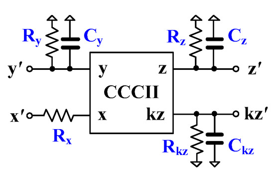
Figure 6.
Parasitic resistances and capacitances of CCCII.
Using (19) and nodal analysis, the denominator (D(s)) of the transfer functions of the filter in Figure 4b can be expressed by
The parameters ωo and in (10) and (11) can be respectively rewritten as
Using (19) and nodal analysis, the denominator (D(s)) of the transfer functions of the filter in Figure 5b can be expressed by
The parameters ωo and in (17) and (18) can be respectively rewritten as
where αj is the voltage gain error, βj, and βkj are the current gain errors of j-th CCCII (j = 1, 2, 3).
From (24) and (25), it can be seen that the voltage gain errors and the current gain errors of CCCIIs will affect the natural frequency and the quality factor of the proposed shadow filters in Figure 4b and Figure 5b. However, this impact can be compensated by electronic tuning.
Considering the proposed shadow filter in Figure 4b by including CCCII with the parasitic components in Figure 6, the denominator of all filtering functions is given by
where CT1 = C1 + Cz-3 + Cy1, CT2 = C2 + Cz-1 + Cy2, G1 = (1/Rz-3)//(1/Ry1), G2 = (1/Rz-1)//(1/Ry2).
The parasitic impedance effects can be made negligible by satisfying the following condition:
The parasitic capacitance will affect the natural frequency and the quality factor that can be expressed respectively by and , where .
Considering the proposed shadow filters in Figure 5b by including the CCCII with the parasitic components in Figure 6, the denominator of all filtering functions is given by
The parasitic impedance effects can be made negligible by satisfying the following condition:
The parasitic capacitance will affect the natural frequency and the quality factor that can be expressed, respectively, by and .
3. Simulation Results
The proposed current-mode shadow filters were simulated using SPICE. The CCCII in Figure 2 was designed with the transistor model parameters of AT&T’s ALA400 CBIC-R process [35]. The DC supply voltage was ±2.5 V. The bias currents Ibi were fixed to 25 μA and the bias current Iai was used to control the current gain ki (i = 1, 2, 3). The simulated performances of the CCCII with controlled current gain used in this paper are given in [36]. The capacitors C1 and C2 were 30 nF.
The first proposed filter in Figure 4b was simulated and the theoretical value was added for comparison. The first simulation was performed with A = 0 (k2 = k3 = 0), by setting the bias currents Ia2 = Ia3 = 0 μA and the bias currents Iset1 = Iset2 = Iset3 = 25 μA. This setting resulted in natural frequency (fo) of 10.2 kHz and the quality factor (Q) of 1. Figure 7 shows the magnitude frequency responses of the LP, HP, BP, and BS filters and Figure 8 shows the magnitude and phase frequency responses of the AP filters. The simulated natural frequency was 10 kHz and was different from the theoretical value by 1.96%. The bandwidth of the filter was approximately 9 MHz.
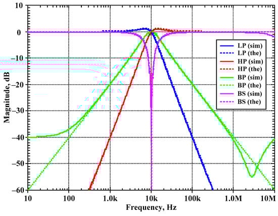
Figure 7.
Simulated magnitude frequency responses of the LP, HP, BP, and BS filters of the first current shadow filter in Figure 4b without modification of the natural frequency and the quality factor (sim = simulation, the = theoretical).
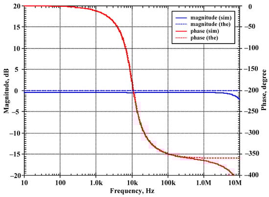
Figure 8.
Simulated magnitude and phase frequency responses of the AP filter of the first current-mode shadow filter in Figure 4b without modification of the natural frequency and the quality factor (sim = simulation, the = theoretical).
Figure 9 shows the magnitude frequency response of the BP filter for different bias currents Iset1 and Iset2 of 5 μA, 15 μA, 50 μA, and 100 μA. The obtained natural frequencies were 1.97 kHz, 5.96 kHz, 19.99 kHz, and 40.22 kHz, respectively. The results of simulations were in close agreement with the theoretical values.
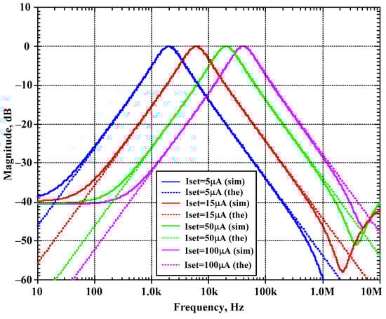
Figure 9.
Simulated magnitude frequency responses of the BP filter of the first current-mode shadow filter in Figure 4b with modification of the natural frequency via the bias currents Iset1 and Iset2 (Iset1 = Iset2 = Iset) and setting the quality factor (Q) to 1 (Q = 1).
Figure 10a–d show the magnitude frequency responses of the LP, HP, BP, and BS filters, respectively, when the quality factor (Q) was changed by k (k = k2 = k3) as Q = 1 (Ia1,2 = 0 μA), Q = 2 (Ia1,2 = 25 μA), Q = 3 (Ia1,2 = 50 μA), Q = 4 (Ia1,2 = 75 μA), and Q = 5 (Ia1,2 = 100 μA) while the bias currents Iset1, Iset2, and Iset3 were set to 25 μA. Figure 11a,b show, respectively, the magnitude and phase frequency responses of the AP filter. Figure 10 and Figure 11 are used to confirm that the shadow filter in Figure 4 can modify the quality factor by the gain k (or A).
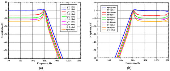
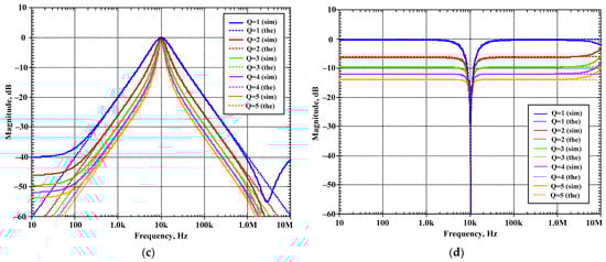
Figure 10.
Simulated magnitude frequency responses of the first current-mode shadow filter in Figure 4b, setting the quality factor by the amplifier k for: (a) LP, (b) HP, (c) BP, and (d) BS.
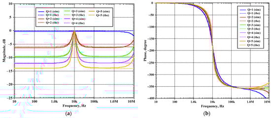
Figure 11.
Simulated frequency responses of AP filter of the first current-mode shadow filter in Figure 4b, setting the quality factor by the amplifier k; (a) magnitude response and (b) phase response.
The second proposed current-mode filter in Figure 5b was simulated and compared with the theory. The first simulation was performed with A2 = 0 (k2 = 0), by setting the bias currents Ia2 = 0 μA and the bias currents Iset1 = Iset2 = Iset3 = 25 μA while the bias current Ia1 was used to control the quality factor (Q) as Q = 1 (Ia1 = 0 μA, k1 = 0), Q = 3 (Ia1 = 16.7 μA, k1 = 0.67), Q = 5 (Ia1 = 20 μA, k1 = 0.8), Q = 7 (Ia1 = 21.5 μA, k1 = 0.86), and Q = 9 (Ia1 = 22.2 μA, k1 = 0.88). Figure 12a–d show the magnitude frequency responses of the LP, HP, BP, and BS filters and Figure 13a,b show, respectively, the magnitude and phase frequency responses of AP filter.
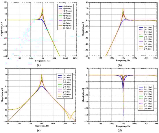
Figure 12.
Simulated magnitude frequency responses of the second current-mode shadow filter in Figure 4b, setting the quality factor by the amplifier k1 with k2 = 0 for: (a) LP, (b) HP, (c) BP, (d) BS.
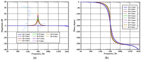
Figure 13.
Simulated frequency responses of the AP filter of the second current-mode shadow filter in Figure 4b, setting the quality factor by the amplifier k1 with k2 = 0; (a) magnitude response and (b) phase response.
The second proposed shadow filter was simulated when the natural frequency was varied by k2 (A2) and k1 (A1) was used for constant Q = 1, and the bias currents Iset1 = Iset2 = Iset3 = 25 μA. Figure 14a–d show the magnitude frequency responses of the LP, HP, BP, and BS filters for fo = 9.37 kHz (k1 = 0.05 (Ia1 = 1.25 μA), k2 = 0.1 (Ia2 = 2.5 μA)), fo = 8.13 kHz (k1 = 0.16 (Ia1 = 4 μA), k2 = 0.3 (Ia2 = 7.5 μA)), fo = 6.69 kHz (k1 = 0.29 (Ia1 = 7.25 μA), k2 = 0.5 (Ia2 = 12.5 μA)), fo = 4.84 kHz (k1 = 0.45 (Ia1 = 11.25 μA), k2 = 0.7 (Ia2 = 17.5 μA)), and fo = 2.93 kHz (k1 = 0.68 (Ia1 = 17 μA), k2 = 0.1 (Ia2 = 22.5 μA)). Figure 15a,b show, respectively, the magnitude and phase frequency responses of the AP filter.
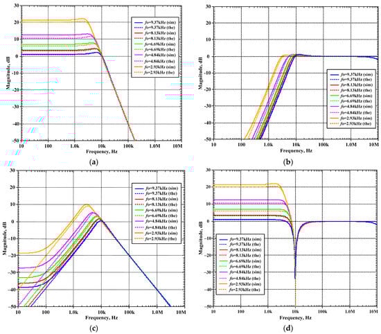
Figure 14.
Simulated magnitude frequency responses of the second current-mode shadow filter in Figure 4b, setting the natural frequency by k2, while k1 is used to adjust Q = 1 for: (a) LP, (b) HP, (c) BP, (d) BS.
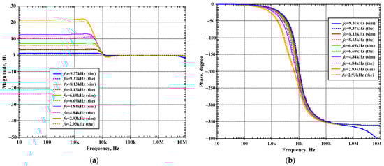
Figure 15.
Simulated frequency responses of AP filter of the second current-mode shadow filter in Figure 4b, setting the natural frequency by k2, while k1 is used to adjust Q = 1; (a) magnitude response and (b) phase response.
Figure 12, Figure 13, Figure 14 and Figure 15 are used to confirm that the quality factor and the natural frequency of the shadow filter in Figure 5 can be modified independently by k1 (or A1) and k2 (or A2), respectively.
To investigate the linearity of the proposed shadow filter in Figure 4b, this filter was simulated with Q = 1 (k2 = k3 = 0, Ia2 = Ia3 = 0 μA), where the amplifier A was not active. Figure 16a shows the input and output waveforms of the LP filter for the frequency of 1 kHz, amplitude of 100 μAp-p, and total harmonic distortion (THD) of 0.937%. Figure 16b shows the simulated THD for the frequency of 1 kHz with different input amplitudes. Figure 16c shows the simulated third intermodulation distortion (IMD3) of the BP filter with a two-tone test, with two closely spaced tones f1 = 9 kHz and f2 = 11 kHz. The IMD3 was less than 1.55% for input amplitude up to 30 μAp-p.
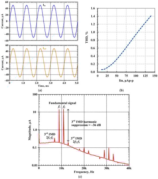
Figure 16.
Simulated distortion of first proposed current-mode shadow filter: (a) the transient response of the LP filter with THD less than 0.937% for Iin = 100 μAp-p, (b) THD of the LP filter with different amplitude of Iin, and (c) IMD3 of the BP filter.
With the condition of Q = 1 and fc = 10 kHz, the proposed current-mode shadow filter in Figure 4b was simulated to investigate the impact of process variations by varying beta (β) in BJT by 10% (LOT tolerance), voltage by varying the supply voltage by ±10%, and temperature (PVT) corners by varying the temperature from −20 to 85 °C. Figure 17a–c show the simulated magnitude frequency responses of the LP, HP, BP, BS, and AP filters for process, voltage, and temperature (PVT) corners, respectively. It can be noted that the natural frequency was affected by the temperature variations. From our investigation, for the temperatures of −20 °C and 85 °C, the natural frequencies were, respectively, 11.09 kHz and 8.81 kHz. Thus, the natural frequency was varied by about ±1.04 kHz.
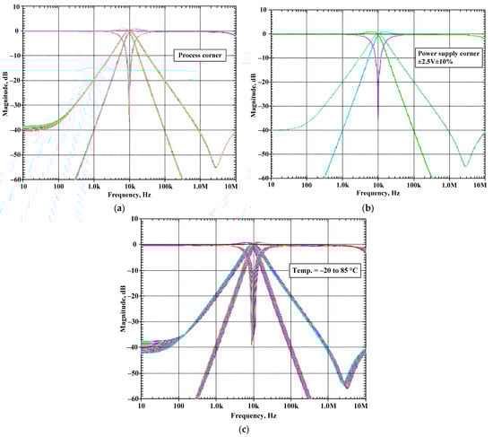
Figure 17.
Simulated magnitude responses of the proposed current-mode shadow filter: (a) process corner, (b) voltage corner, and (c) temperature corner.
The BP response was simulated by setting 5% tolerances of the capacitor C1 and C2 at the cut-off frequency of 10 kHz and 200 Gaussian distribution runs. Figure 18 shows the derived histogram of the center frequency. The standard deviation () of fo was 0.317 kHz and the maximum and minimum values of fo were, respectively, 10.805 kHz and 9.231 kHz.
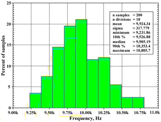
Figure 18.
The histogram of the center frequency of the BP filter with 200 runs of MC analysis.
The proposed current-mode shadow filters were compared with previous shadow filters in Table 1. The voltage-mode shadow filters in [15,22], the current-mode shadow filters in [27,28,30], and the multi-mode shadow filters in [34] were selected for comparison. Compared with [22,27,28], the proposed filter can provide five filtering functions of LP, HP, BP, BS, and AP filters. Compared with [15,30], the proposed filter does not possess a buffer circuit at input or output terminals. Compared with [15,34], the proposed filter has no resistors and has a simpler structure. As can be seen, the proposed filters have the following features which the others do not: they offer the highest number of responses without the need for a buffer circuit at the input and output, have no resistors, all capacitors are grounded, and they have the possibility of electronic tuning of the natural frequency and quality factor.

Table 1.
Comparison of the proposed design with previous works.
4. Experimental Results
To confirm the functionality of the proposed shadow filters, an experimental setup of CCCII was designed using commercially available 2N3904 (NPN) and 2N3906 (PNP) transistors with supply voltage of ±2.5 V. Figure 19 shows the experimental setup for the current-mode shadow filter. Passive capacitors were chosen as C1 = C2 = 330 nF and passive resistors 10 kΩ were used for voltage-to-current (V-I) converter as input and current-to-voltage (I-V) converter as output. The resistor that was connected in series with terminal Iin works as a V-I converter to convert the voltage signal from the function generator to the current signal Iin and the grounded resistors that were connected to terminals ILP, IHP, IBP, IBS, and IAP were used as I-V converter to convert current signals to voltage signals. The input and output waveforms ware measured using a KEYSIGHT DSOX1204G oscilloscope; the input signal was also provided by this oscilloscope.
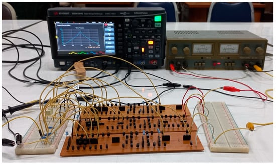
Figure 19.
Experimental setup for proposed shadow filters.
The experimental frequency responses of the shadow filter in Figure 4b without modification of the natural frequency and the quality factor (A = 0, Q = 1) of (a) LP, (b) HP, (c) BP, (d) BS, and (e) AP are shown in Figure 20. Figure 21 shows the experimental frequency responses of the shadow filter in Figure 4b upon setting the quality factor of the amplifier A ≈ 3 of (a) LP, (b) HP, (c) BP, (d) BS, (e) AP.
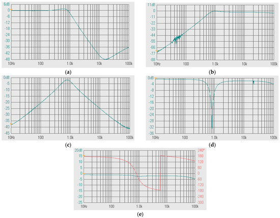
Figure 20.
Experimental frequency responses of the first shadow filter in Figure 4b without modification of the natural frequency and the quality factor (A = 0, Q = 1) of (a) LP, (b) HP, (c) BP, (d) BS, and (e) AP.
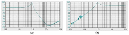
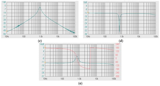
Figure 21.
Experimental frequency responses of the first shadow filter in Figure 4b, setting the quality factor by the amplifier A ≈ 3 of (a) LP, (b) HP, (c) BP, (d) BS, (e) AP.
Figure 22 shows the experimental frequency responses of the second shadow filter in Figure 5b, setting the quality factor by the amplifier k1 with k2 = 0 for: (a) LP, (b) HP, (c) BP, (d) BS. Figure 23 shows the experimental frequency responses of the second shadow filter in Figure 5b, setting the natural frequency by k2, while k1 is used to adjust Q for (a) LP, (b) HP, (c) BP, (d) BS, (e) AP.
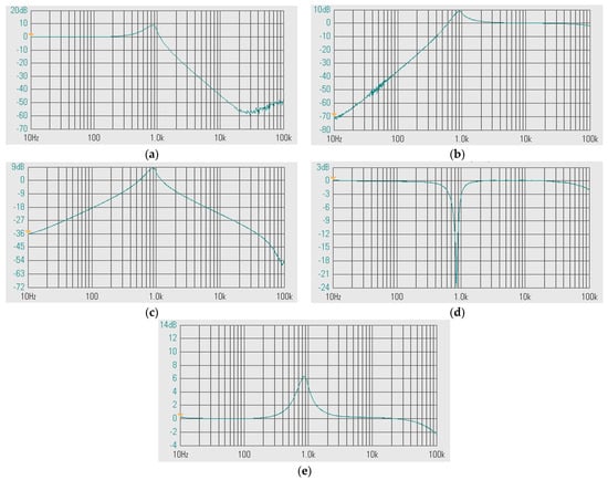
Figure 22.
Experimental frequency responses of the second current-mode shadow filter in Figure 5b setting the quality factor by the amplifier k1 with k2 = 0 for: (a) LP, (b) HP, (c) BP, (d) BS, and (e) AP.
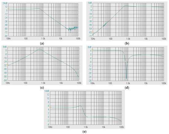
Figure 23.
Experimental frequency responses of the second shadow filter in Figure 5b, setting the natural frequency by k2, while k1 is used to adjust Q for: (a) LP, (b) HP, (c) BP, (d) BS, (e) AP.
5. Conclusions
This paper proposes two current-mode shadow filters using CCCIIs with controlled current gains. The circuits employ three CCCIIs with controlled current gains and two grounded capacitors. The proposed architecture can realize LP, HP, BP, BS, and AP filters in the same topology. The current gains of CCCIIs can be used to modify the natural frequency and the quality factor of all filtering functions. The proposed shadow filters have the advantages of low-input and high-output impedances and low circuit complexity; they do not require passive resistors; they are suitable for integrated circuits by using grounded capacitors; and they have electronic tuning capability. To show the workability and performance of the proposed filters, SPICE simulation was performed. The simulated results were in agreement with the theoretical values and the experimental results confirm the functionality and the performance of the proposed filters.
Author Contributions
Conceptualization, M.K. (Montree Kumngern), F.K. and T.K.; methodology, M.K. (Montree Kumngern), F.K., B.K. and S.L.; software, M.K. (Montree Kumngern), B.K. and S.L.; validation, M.K. (Montree Kumngern), F.K.; formal analysis, M.K. (Montree Kumngern); investigation, M.K. (Martin Kyselak), F.K. and T.K.; resources, M.K. (Martin Kyselak); data curation, M.K. (Martin Kyselak) and F.K.; writing—original draft preparation, M.K. (Montree Kumngern), F.K., B.K. and S.L.; writing—review and editing, M.K. (Montree Kumngern), F.K., B.K., S.L. and T.K.; visualization, M.K. (Martin Kyselak) and M.K. (Montree Kumngern); supervision, M.K. (Montree Kumngern) and F.K.; project administration, M.K. (Montree Kumngern) and F.K.; funding acquisition, M.K. (Montree Kumngern). All authors have read and agreed to the published version of the manuscript.
Funding
This work was supported in part by the University of Defence within the Organization Development Project VAROPS, and by the School of Engineering, King Mongkut’s Institute of Technology Ladkrabang, under Grant 2565-02-01-005.
Institutional Review Board Statement
Not applicable.
Informed Consent Statement
Not applicable.
Data Availability Statement
Data are contained within the article.
Conflicts of Interest
The authors declare no conflicts of interest.
References
- Roberts, G.; Sedra, A. All-current-mode frequency selective circuits. Electron. Lett. 1989, 25, 759–761. [Google Scholar] [CrossRef]
- Toumazou, C.; Lidgey, F.J.; Haig, D.G. Analogue IC Design: The Cur-Rent-Mode Approach; Peter Peregrinus: London, UK, 1990. [Google Scholar]
- Sedra, A.; Smith, K. A second-generation current conveyor and its applications. IEEE Trans. Circuit Theory 1970, 17, 132–134. [Google Scholar] [CrossRef]
- Fabre, A.; Saaid, O.; Wiest, F.; Boucheron, C. Current controlled bandpass filter based on translinear conveyors. Electron. Lett. 1995, 31, 1727–1728. [Google Scholar] [CrossRef]
- Fabre, A.; Mimeche, N. Class A/AB second generation current conveyor with controlled current gain. Electron. Lett. 1996, 43, 82–91. [Google Scholar] [CrossRef]
- Surakampontorn, W.; Kumwachara, K. CMOS-based electronically tunable current conveyor. Electron. Lett. 1992, 28, 1316–1317. [Google Scholar] [CrossRef]
- Mimaei, S.; Sayin, O.K.; Kuntman, H. A New CMOS electronically tunable current conveyor and its application to current-mode fil-ters. IEEE Trans. Circuits Syst. I Regul. Pap. 2006, 53, 1448–1458. [Google Scholar] [CrossRef]
- Lakys, Y.; Fabre, A. Shadow filters–new family of second-order filters. Electron. Lett. 2010, 46, 276–277. [Google Scholar] [CrossRef]
- Biolkova, V.; Biolek, D. Shadow filters for orthogonal modification of characteristic frequency and bandwidth. Electron. Lett. 2010, 46, 830–831. [Google Scholar] [CrossRef]
- Anurag, R.; Pandey, R.; Pandey, N.; Singh, M.; Jain, M. OTRA based shadow filters. In Proceedings of the 2015 Annual IEEE India Conference (INDICON), New Delhi, India, 17–20 December 2015; pp. 1–4. [Google Scholar] [CrossRef]
- Abuelma’Atti, M.T.; Almutairi, N. New voltage-mode bandpass shadow filter. In Proceedings of the 2016 13th International Multi-Conference on Systems, Signals & Devices (SSD), Leipzig, Germany, 21–24 March 2016; pp. 412–415. [Google Scholar] [CrossRef]
- Abuelma’Atti, M.T.; Almutairi, N. New CFOA-based shadow bandpass filter. In Proceedings of the 2016 International Conference on Electronics, Information, and Communications (ICEIC), Danang, Vietnam, 27–30 January 2016; pp. 1–3. [Google Scholar] [CrossRef]
- Abuelma’atti, M.T.; Almutairi, N.R. Almutairi. New current-feedback operational-amplifier based shadow filters. Analog. Integr. Circuits Signal Process. 2016, 86, 471–480. [Google Scholar] [CrossRef]
- Alaybeyoğlu, E.; Kuntman, H. CMOS implementations of VDTA based frequency agile filters for encrypted communications. Analog. Integr. Circuits Signal Process. 2016, 89, 675–684. [Google Scholar] [CrossRef]
- Huaihongthong, P.; Chaichana, A.; Suwanjan, P.; Siripongdee, S.; Sunthonkanokpong, W.; Supavarasuwat, P.; Jaikla, W.; Khateb, F. Single-input multiple-output voltage-mode shadow filter based on VDDDAs. AEU-Int. J. Electron. Commun. 2019, 103, 13–23. [Google Scholar] [CrossRef]
- Buakaew, S.; Narksarp, W.; Wongtaychatham, C. Fully active and minimal shadow bandpass filter. In Proceedings of the 2018 International Conference on Engineering, Applied Sciences, and Technology (ICEAST), Phuket, Thailand, 4–7 July 2018; pp. 1–4. [Google Scholar] [CrossRef]
- Buakaew, S.; Narksarp, W.; Wongtaychatham, C. Shadow bandpass filter with Q-improvement. In Proceedings of the 2019 5th International Conference on Engineering, Applied Sciences and Technology (ICEAST), Luang Prabang, Laos, 2–5 July 2019; pp. 1–4. [Google Scholar] [CrossRef]
- Buakaew, S.; Narksarp, W.; Wongtaychatham, C. High quality-factor shadow bandpass filters with orthogonality to the characteristic frequency. In Proceedings of the 2020 17th International Conference on Electrical Engineering/Electronics, Computer, Telecommunications and Information Technology (ECTI-CON), Phuket, Thailand, 24–27 June 2020; pp. 372–375. [Google Scholar] [CrossRef]
- Moonmuang, P.; Pukkalanun, T.; Tangsrirat, W. Voltage differencing gain amplifier-based shadow filter: A comparison study. In Proceedings of the 2020 6th International Conference on Engineering, Applied Sciences and Technology (ICEAST), Chiang Mai, Thailand, 1–4 July 2020; pp. 1–4. [Google Scholar] [CrossRef]
- Buakaew, S.; Wongtaychatham, C. Boosting the quality factor of the shadow bandpass filter. J. Circuits Syst. Comput. 2022, 31, 2250248. [Google Scholar] [CrossRef]
- Varshney, G.; Pandey, N.; Pandey, R. Generalization of shadow filters in fractional domain. Int. J. Circuit Theory Appl. 2021, 49, 3248–3265. [Google Scholar] [CrossRef]
- Khateb, F.; Kumngern, M.; Kulej, T.; Ranjan, R.K. 0.5 V multiple-input multiple-output differential difference transconductance amplifier and its applications to shadow filter and oscillator. IEEE Access 2023, 11, 31212–31227. [Google Scholar] [CrossRef]
- Pandey, N.; Pandey, R.; Choudhary, R.; Sayal, A.; Tripathi, M. Realization of CDTA based frequency agile filter. In Proceedings of the 2013 IEEE International Conference on Signal Processing, Computing and Control (ISPCC), Solan, India, 26–28 September 2013; pp. 1–6. [Google Scholar] [CrossRef]
- Pandey, N.; Sayal, A.; Choudhary, R.; Pandey, R. Design of CDTA and VDTA based frequency agile filters. Adv. Electron. 2014, 2014, 176243. [Google Scholar] [CrossRef]
- Alaybeyoğlu, E.; Güney, A.; Altun, M.; Kuntman, H. Design of positive feedback driven current-mode amplifiers Z-Copy CDBA and CDTA, and filter applications. Analog. Integr. Circuits Signal Process. 2014, 81, 109–120. [Google Scholar] [CrossRef]
- Atasoyu, M.; Kuntman, H.; Metin, B.; Herencsar, N.; Cicekoglu, O. Design of current-mode class 1 frequency-agile filter employing CDTAs. In Proceedings of the 2015 European Conference on Circuit Theory and Design (ECCTD), Trondheim, Norway, 24–26 August 2015; pp. 1–4. [Google Scholar] [CrossRef]
- Alaybeyoğlu, E.; Kuntman, H. A new frequency agile filter structure employing CDTA for positioning systems and secure communications. Analog. Integr. Circuits Signal Process. 2016, 89, 693–703. [Google Scholar] [CrossRef]
- Nand, D.; Pandey, N. New Configuration for OFCC-Based CM SIMO Filter and its Application as Shadow Filter. Arab. J. Sci. Eng. 2018, 43, 3011–3022. [Google Scholar] [CrossRef]
- Chhabra, K.; Singhal, S.; Pandey, N. Realisation of CBTA based current mode frequency agile filter. In Proceedings of the 2019 6th International Conference on Signal Processing and Integrated Networks (SPIN), Noida, India, 7–8 March 2019; pp. 1076–1081. [Google Scholar] [CrossRef]
- Singh, D.; Paul, S.K. Realization of current mode universal shadow filter. AEU-Int. J. Electron. Commun. 2020, 117, 153088. [Google Scholar] [CrossRef]
- Singh, D.; Paul, S.K. Improved current mode biquadratic shadow universal filter. Inf. MIDEM 2022, 52, 51–66. [Google Scholar] [CrossRef]
- Nand, D.; Pandey, N.; Bhanoo, V.; Gangal, A. Operational floating current conveyor based TAM & TIM shadow filter. In Proceedings of the 4th International Conference on Computer and Management (ICCM), New Delhi, India, 22–23 December 2018; pp. 103–115. [Google Scholar]
- Singh, D.; Paul, S.K. Mixed-mode universal filter using FD-CCCTA and its extension as shadow filter. Inf. MIDEM 2022, 52, 239–262. [Google Scholar] [CrossRef]
- Singh, D.; Sajai, P.K. Realization of multi-mode universal shadow filter and its application as a frequency-hopping filter. Mem.-Mater. Devices Circuits Syst. 2023, 4, 100049. [Google Scholar] [CrossRef]
- Frey, D.R. Log domain filter: An approach to current mode filtering. IEE Proc. Part G Circuits Devices Syst. 1993, 140, 406–416. [Google Scholar] [CrossRef]
- Kumngern, M.; Jongchanachavawat, W.; Phatsornsiri, P.; Wongprommoon, N.; Khateb, F.; Kulej, T. Current-mode first-order versatile filter using translinear current conveyors with controlled current gain. Electronics 2023, 12, 2828. [Google Scholar] [CrossRef]
Disclaimer/Publisher’s Note: The statements, opinions and data contained in all publications are solely those of the individual author(s) and contributor(s) and not of MDPI and/or the editor(s). MDPI and/or the editor(s) disclaim responsibility for any injury to people or property resulting from any ideas, methods, instructions or products referred to in the content. |
© 2024 by the authors. Licensee MDPI, Basel, Switzerland. This article is an open access article distributed under the terms and conditions of the Creative Commons Attribution (CC BY) license (https://creativecommons.org/licenses/by/4.0/).