Article

an-QNA: An Adaptive Nesterov Quasi-Newton Acceleration-Optimized CMOS LNA for 65 nm Automotive Radar Applications

1
Department of Smart Robot Convergence and Application Engineering, Pukyong National University, Busan 48513, Republic of Korea
2
Department of Electronics & Communication Engineering, JB Institute of Engineering & Technology, (Autonomous), Hyderabad 500075, India
3
Department of Spatial Information Engineering, Pukyong National University, Busan 48513, Republic of Korea
*
Authors to whom correspondence should be addressed.
These authors contributed equally to this work.
Sensors 2024, 24(18), 6141; https://doi.org/10.3390/s24186141
Submission received: 20 August 2024 / Revised: 20 September 2024 / Accepted: 20 September 2024 / Published: 23 September 2024
(This article belongs to the Special Issue CMOS Integrated Circuits for Sensor Applications)

Abstract

:
An adaptive Nesterov quasi-Newton acceleration (an-QNA)-optimized low-noise amplifier (LNA) is proposed in this paper. An optimized single-ended-to-differential two-stage LNA circuit is presented. It includes an improved post-linearization (IPL) technique to enhance the linearity. Traditional methods like conventional quasi-Newton (c-QN) often suffer from slow convergence and the tendency to get trapped in local minima. However, the proposed an-QNA method significantly accelerates the convergence speed. Furthermore, in this paper, modifications have been made to the an-QNA algorithm using a quadratic estimation to guarantee global convergence. The optimized an-QNA-based LNA, using standard 65 nm CMOS technology, achieves a simulated gain of 17.5 dB, a noise figure (NF) of 3.7 dB, and a 1 dB input compression point (IP1dB) of −13.1 dBm. It is also noted that the optimized LNA achieves a measured gain of 12.9 dB and an NF of 4.98 dB, and the IP1dB is −17.8 dB. The optimized LNA has a chip area of 0.67 mm2.

1. Introduction

A complementary metal-oxide semiconductor (CMOS) is a fundamental technology used to make integrated circuits (ICs), such as microprocessors and microcontrollers. Over the years, CMOS technology has improved tremendously. A big breakthrough in RF (radio frequency) and mixed-signal IC design came with the combination of low-noise amplifiers (LNAs) and CMOS technology [1]. The LNA is a key component of automotive radar systems. Automotive radars operate primarily at frequencies around 24 GHz [2]. Figure 1 represents the overview of RF transceiver, and Figure 2 represents the radar application.
The challenge, however, remains to design CMOS LNA for automotive radar systems. We are still in the early stages of designing and automating LNA circuits. The design of the LNA becomes more difficult when it works at high frequencies [3]. The high non-linearity of its parameters means that the researchers have a hard time designing a high-performance economic circuit on their own due to non-linearity. Additionally, the design of optimal LNAs for automotive radars is challenging because they must have wide bandwidths, low noise levels, and high linearity in order to pick up weak signals while ignoring strong ones. In order to achieve a delicate balance between these two tenets, intricate design optimizations would be necessary along with multidisciplinary expertise in RF circuitry and multilevel considerations at the system level.
From the prior research, it is evident that optimization algorithms (OAs) [4] play a significant role in the design process. Recent advances in intelligent paradigm research have led to a number of theoretical advancements and to successful applications of intelligent techniques and approaches to a variety of fields [5,6]. In many optimization problems, linear programming [7], Newton’s method [8], gradient search methods [9], quadratic programming, and nonlinear programming [10] are used. The issue of LNA circuits has been addressed in the literature by many optimization techniques, including genetic algorithms (GA) [11], particle swarm optimization (PSO) [12], flower pollination [13], firefly algorithms (FA) [14], ant colony (AC) [15], and artificial bee colony (ABC) [16].
The PSO method was used by Thakker and Fakhfakh et al. [17,18] for the automatic sizing of low-power analog circuits, the automatic synthesis of LNA [19], and the design of microwave filters [20]. It has been shown that a GA can be used to optimize several electrical parameters of LNAs [21]. In [22,23], for analog and RF circuit a highly efficient parasitic aware hybrid sizing methodology is proposed. According to Yiming Li et al. [24] GA generalizes the method for optimizing parameters for LNA circuits with respect to constraints. However, the paper has limitations, as using a small population size could result in unsatisfactory convergence behavior. A recent report [25,26] also noted optimized design parameters for LNAs using PSO. As demonstrated in [27], the iterative loop between the OAs and the performance evaluator allows the multi-objective artificial bee colony (MOABC) algorithm to optimize the voltage gain and noise figure.
In order to accelerate the process of convergence to the global maximum, Khong et al. [28] used direct global optimization techniques to implement a multi-unit algorithm. According to Shams et al. [29], several parameters of the LNA were optimized using GSA, including S21, S11, S22, S12, and the noise figure (NF). GSA’s clustered GSA (CGSA) has been successfully exploited to reduce computational complexity, improve efficiency, and improve robustness. In [30,31], genetic computation was utilized to circumvent parasitics and achieve optimal results, but no mathematical analysis was provided. A cascade LNA was designed and optimized using PSO [32].
As part of our work, we chose adaptive Nesterov quasi-Newton acceleration (an-QNA) to optimize LNA at 24 GHz. An-QNA benefits high-frequency applications because it can be converged and optimized more quickly. With an-QNA, optimization processes are smoother, and convergence is faster. Evolutionary algorithms (EAs), however, may be preferred when the optimization is highly non-linear and non-convex or when the exploration of unconventional design spaces is required, though they may be slower to reach convergence. In contrast to conventional quasi-Newton (c-QN), which usually struggles with slow convergence and gets stuck in local minima, an-QNA guarantees faster global convergence. We have made modifications to the an-QNA algorithm to guarantee global convergence. Therefore, in the fair comparison in our work, we compare c-QN with the proposed an-QNA to optimize the 24 GHz LNA.

Main Contributions

In the following list, we summarize and discuss the paper’s main contributions:
1. The paper presents an an-QNA designed to improve the performance of LNAs. The proposed an-QNA significantly accelerates the convergence speed compared to c-QN, which often suffer from slow convergence and local minima issues.
2. The proposed LNA circuit includes an improved post-linearization (IPL) technique. This technique enhances the linearity of the LNA, a critical factor in achieving high-performance automotive radar applications.
3. In the proposed an-QNA, we have made modifications using a quadratic estimation to the an-QNA algorithm to ensure global convergence, addressing a significant challenge in OAs used in circuit design.
4. Utilizing standard 65 nm CMOS technology, the optimized LNA achieves a simulated gain of 17.5 dB and an NF of 3.7 dB as well as a 1 dB input compression point (IP1dB) of −13.1 dBm. Furthermore, the optimized LNA achieves a measured gain of 12.9 dB and an NF of 4.98 dB in addition to an IP1dB of −17.8 dB.
This paper consists of four sections. The proposed LNA circuit using an-QNA is described in Section 2. The simulation results are presented in Section 3, and in Section 4, the conclusions and future research directions are given.

2. Proposed Methodology for Optimizing an LNA Circuit

2.1. Adaptive Nesterov Quasi-Newton Acceleration (an-QNA)

an-QNA is an OA algorithm that combines the concepts of Nesterov’s acceleration with quasi-Newton methods while introducing adaptivity to improve convergence speed and efficiency. c-QN methods are a class of OAs used to find the minimum (or maximum) of a function. In comparison to c-QN, the an-QNA convergence process is much faster.

2.2. Modifications in an-QNA

To achieve a faster convergence in an-QNA, we included a quadratic estimation at wi + μ zi. Additionally, we added Nesterov’s enhanced gradient, namely ∇F (wi + μ zi). The an-QNA modification is briefly outlined as follows. In our work, we consider Equations (1)–(3),
F w = 1 T r p ϵ T r F p w
F p w = 1 2 d p o p 2
F w F w i + μ i z i + F w i + μ i T w + 1 2 w T 2 F w i + μ i z i w
There is a precise minimization of this quadratic function in Equation (4),
w = 2 F w i + μ i z i 1 F w i + μ i z i
It is considered as Newton’s method with momentum added μ zi in Equation (5).
w i + 1 = w i + μ i z i 2 F w i + μ i z i 1 F w i + μ i z i
The inverse of Hessian in Equation (6), ∇F (wi + μ izi) is estimated by the matrix Hi+1,
H ^ i + 1 = ( I ρ i ^ s i r i T ) H ^ i I ρ i s i r i T + ρ i s i r i T
where
si = wi+1 − (wi + μ izi)
ri = ∇F(wi+1) F(wi + μ izi),
Then, the renew vector of an-QNA can be written as in Equations (7) and (8),
z i + 1 = μ i z i α i g ^ i
g i ^ = H ^ i F w i z i
Thus, the vector in the modified method is given as in Equations (9) and (10),
ξ ^ i = w F w i + μ z i + m a x ϵ i T s i s i 2 , 0
ω = 2 i f   F w i + μ z i 2 > 10 2 ω = 100 i f   F w i + μ z i 2 < 10 2
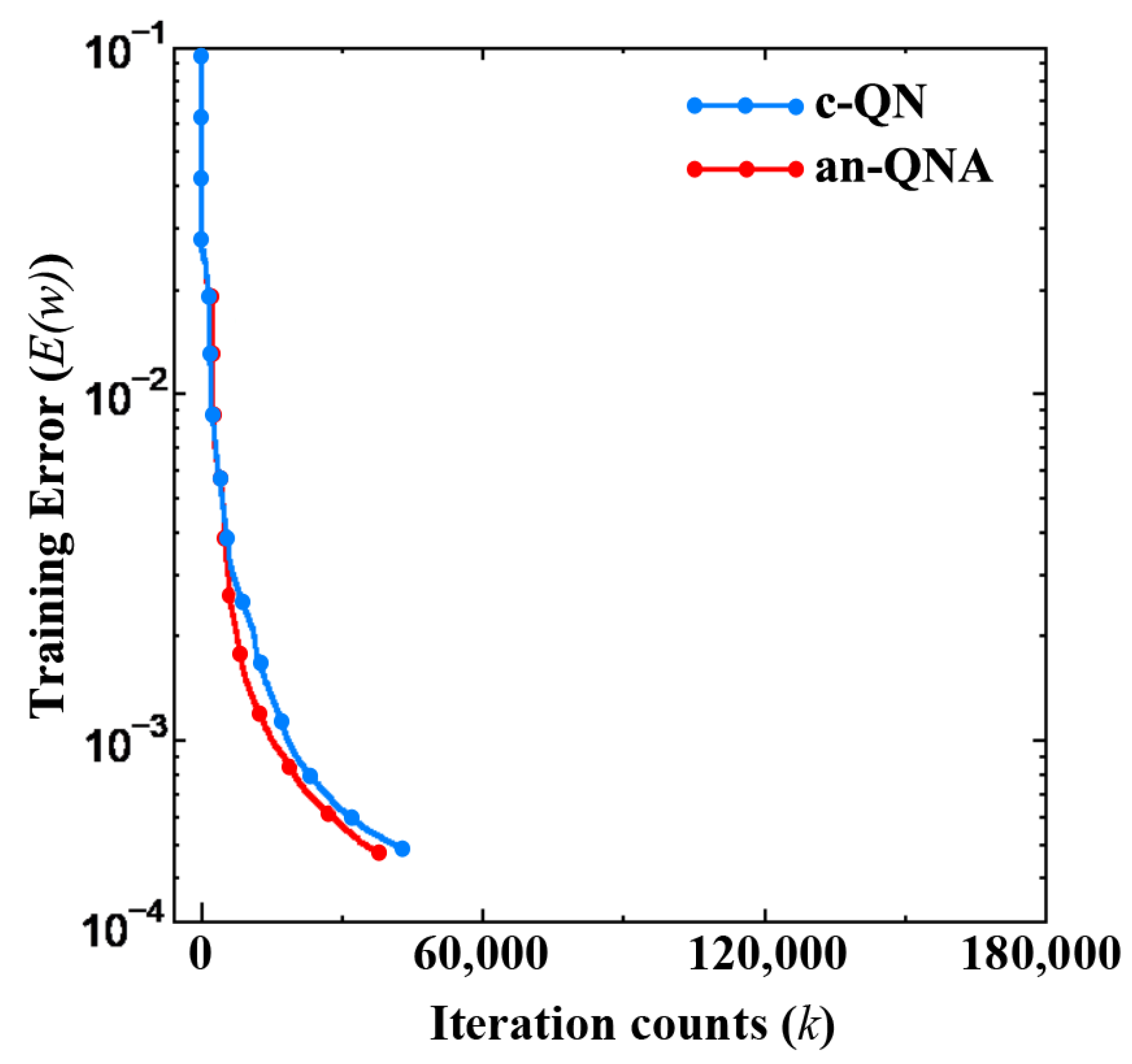
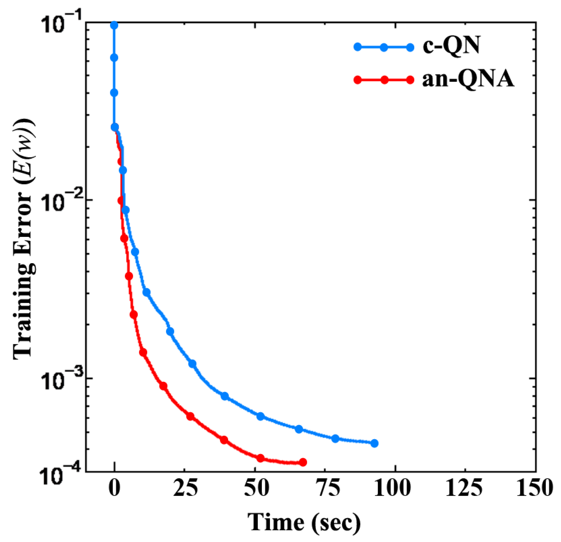
Figure 3 presents the training error vs. iteration counts of LNA, while Figure 4 shows LNA training error vs. time. Table 1 presents the summary of the simulation results of LNA modeling. From Table 1, we can see that the convergence rate for c-QN is 75% while the convergence rate of the proposed an-QNA is 100%. On the other hand, the c-QN’s execution time is 65 s, and the proposed an-QNA’s execution time is 95 s.

2.3. Convergence Performance Analysis of an-QNA

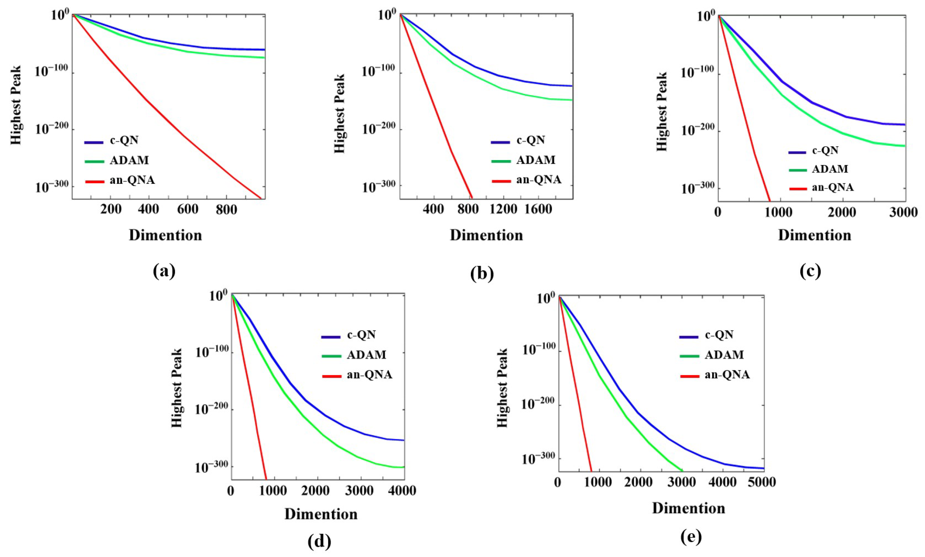
In this section, Equations (11)–(18) represent eight benchmark functions, both unimodal and multimodal, which are employed to assess the performance of the an-QNA algorithm. Table 2, provides detailed information regarding the dimensions, minimum range, and function characteristics of these benchmark functions. The performance of gradient-based OAs such as c-QN and adaptive moment estimation (ADAM) has been evaluated alongside the an-QNA variant to examine aspects like convergence rate, stability, and computational accuracy across multiple iterations, as depicted in Figure 5. The results demonstrate that, when comparing the optimal function values plotted over several generations in Figure 5, the an-QNA variant outperforms others in terms of convergence, particularly in scenarios with models of varying sizes, ranging from 1000 to 5000 dimensions. The graphs indicate that for the an-QNA variants, the standard test function values decrease rapidly as the number of generations increases, in contrast to other OAs. In Figure 5, it can be observed that both c-QN and ADAM exhibit slow convergence and tend to stagnate during the partitioning process. However, the an-QNA variant, particularly in terms of the mean strategy, effectively prevents the algorithm from getting trapped in local minima and enhances the search process by speeding up convergence.
F u n c t i o n v 1 u n i m o d a l y = i = 1 n y i 2
F u n c t i o n v 1 u n i m o d a l y = i = 1 n j 1 n y j 2
F u n c t i o n v 3 u n i m o d a l y = i = 1 n y i + 0.5 2
F u n c t i o n v 4 u n i m o d a l y = i = 1 n i y i 4 + r a n d 0 , 1
F u n c t i o n v 5 m u l t i m o d a l y = i = 1 n y i s i n | y i |
F u n c t i o n v 6 m u l t i m o d a l y = 20 e x p 0.2 1 n i = 1 n y i 2 e x p 1 n i = 1 n c o s 2 π y i + 20 + e
F u n c t i o n v 7 m u l t i m o d a l y = i = 1 n y i 2 10 c o s 2 π y i + 10
F u n c t i o n v 8 m u l t i m o d a l y = i = 1 n y i 2 10 c o s 2 π y i + 10
F u n c t i o n v 8 m u l t i m o d a l y = 1 4000 i = 1 n i = 1 n c o s y i i + 1
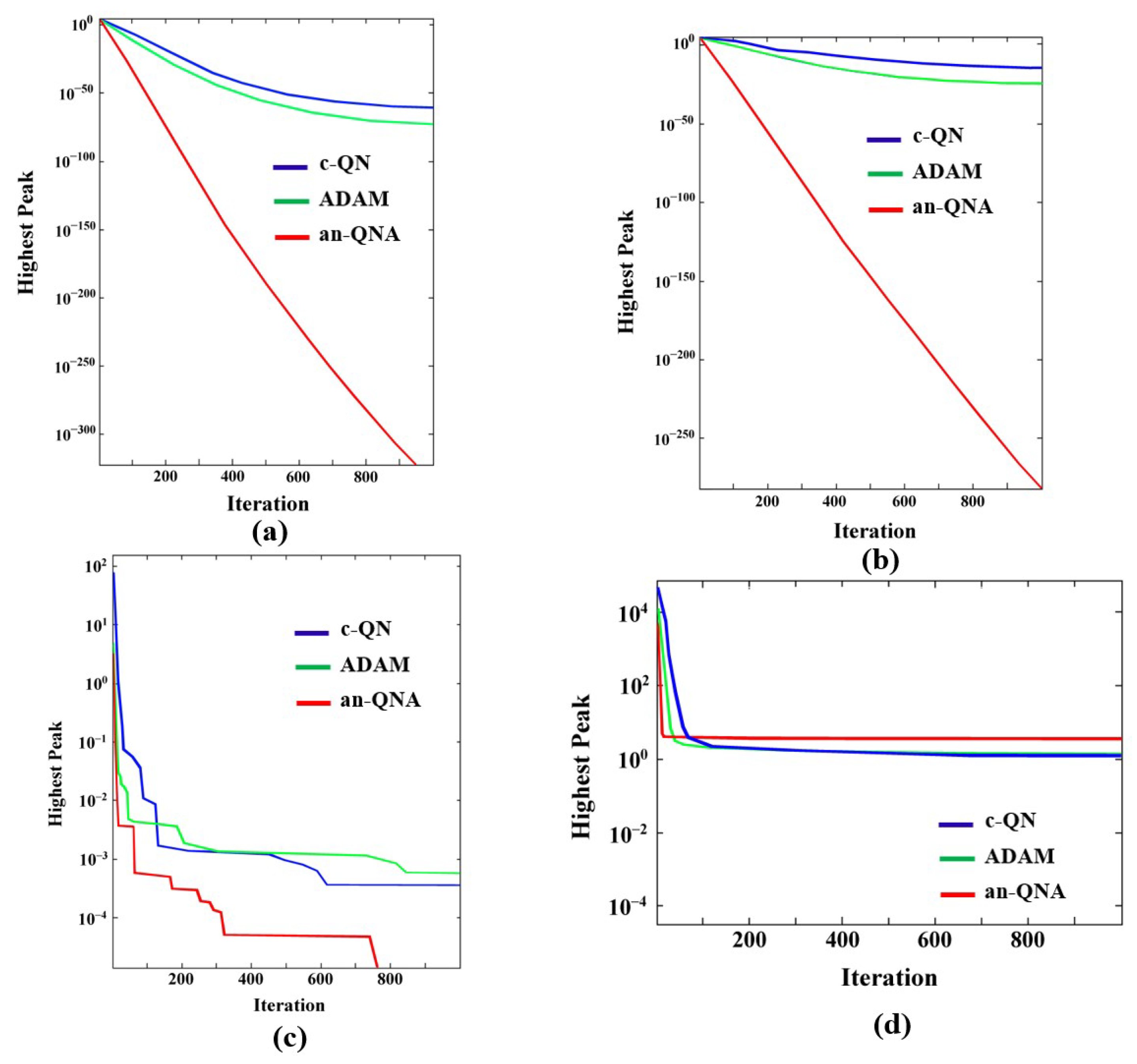
The c-QN, ADAM, and an-QNA algorithms were developed using MATLAB R2021a. Table 3, Table 4 and Table 5 indicate that the c-QN, ADAM, and an-QNA algorithms deliver the best optimal values for classical optimization problems in terms of the minimum and maximum function values compared to other OAs. Meanwhile, Table 6, Table 7 and Table 8 show that the an-QNA outperforms c-QN and ADAM in terms of producing higher-quality standard and mean values for most classical functions, yielding the smallest function values. Additionally, the convergence graphs in Figure 6 and Figure 7 demonstrate that an-QNA achieves the best possible optimal values for standard functions in fewer iterations than c-QN and ADAM. The results presented in Table 6, Table 7 and Table 8 clearly show that the proposed an-QNA variant surpasses the performance of other algorithms, including c-QN and ADAM, in terms of mean, standard deviation, and minimum/maximum cost function values while efficiently finding the optimum. Therefore, the an-QNA variant proves to be highly competitive with other OAs.
Furthermore, the convergence behaviors of c-QN, ADAM, and the proposed an-QNA algorithms have been analyzed, with the convergence curves depicted in Figure 6 and Figure 7. These curves reveal that the an-QNA consistently achieves better convergence points than the other algorithms. The obtained results confirm that the an-QNA is more effective in identifying the best optimal solution with fewer iterations. As a result, the an-QNA algorithm successfully avoids premature convergence to local optima and enhances the exploration of the search space.

3. Proposed an-QNA Based LNA Circuit

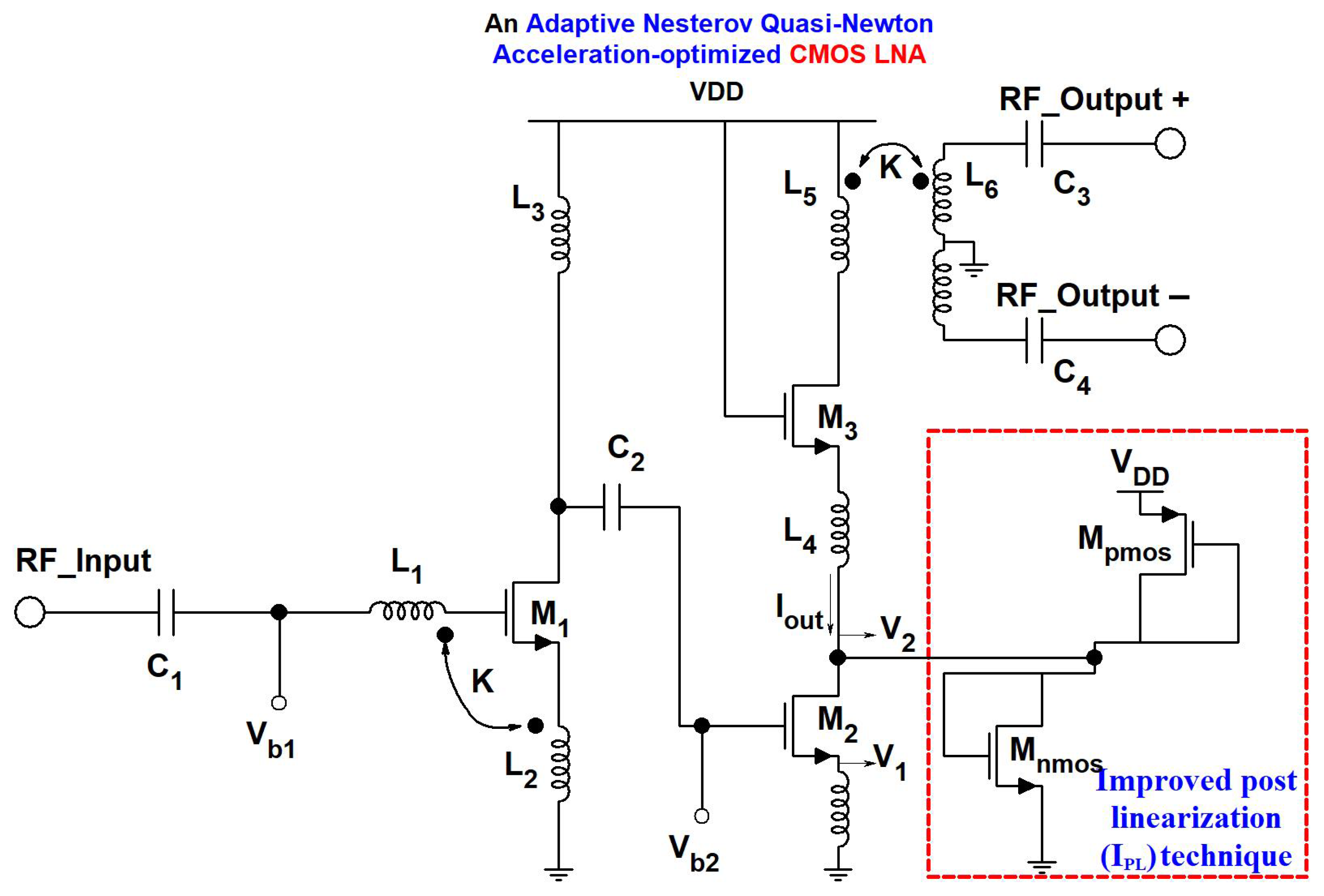
The schematic of the proposed single-ended-to-differential LNA using an-QNA is shown in Figure 8. The designed LNA is composed of two stages. The first stage includes the transistor in a common-source configuration, and the second stage of the LNA includes a common-source transistor cascoded with a common-gate transistor. An improved post-linearization (IPL) technique is implemented to mitigate the non-linearity of the designed LNA. Table 9 shows the proposed LNA device component values using an-QNA.
An input matching of the designed LNA consists of a feedback transformer formed by the coupling of L1 and L2. The input impedance of the amplifier is approximately given by Equation (20):
Z i n 1 g m n k 2 n k + 1
where gm refers to the transconductance of the transistor M1,
n = L 1 L 2
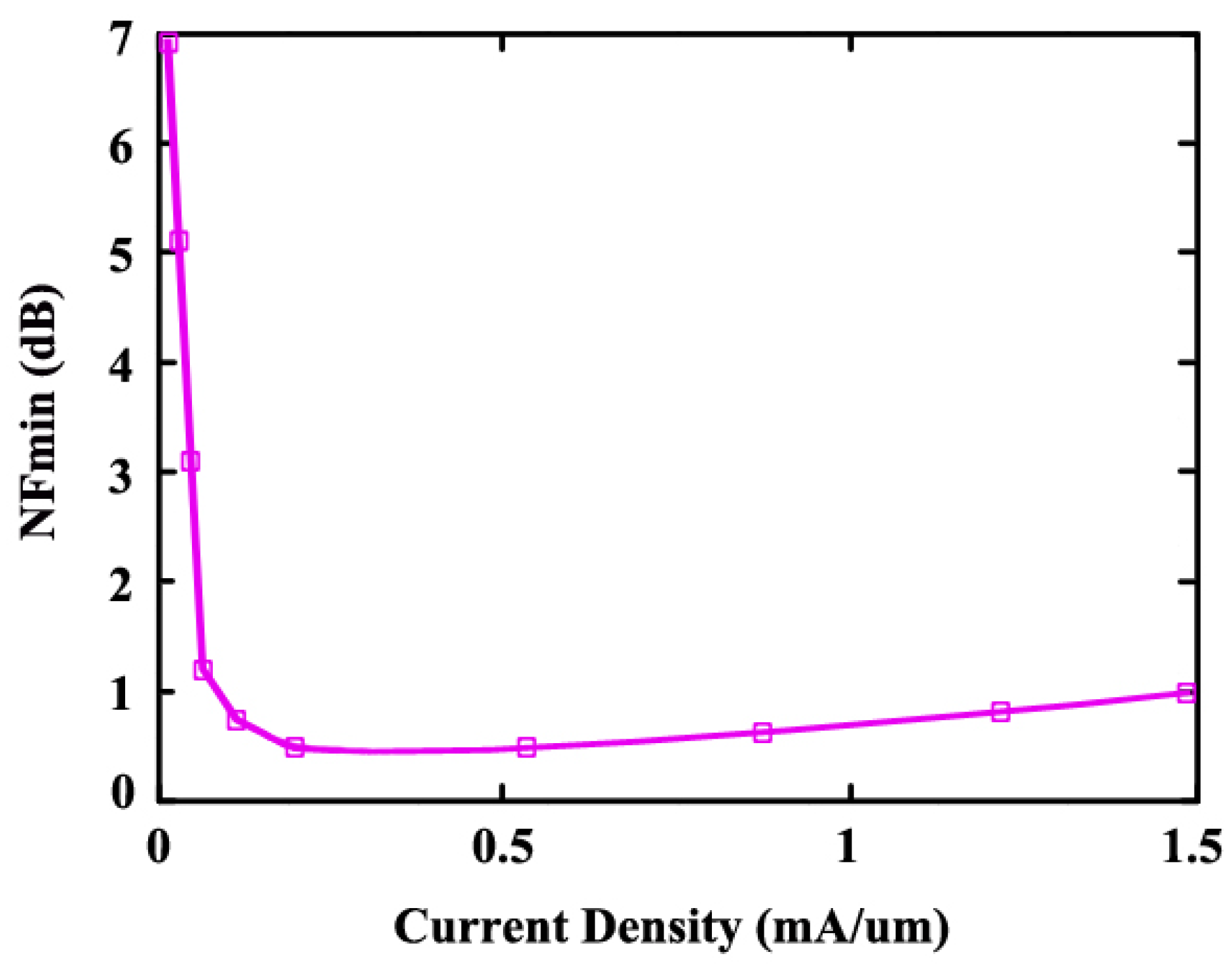
Here, n is the turns ratio, and k is the coupling factor. The input matching is shown by Equation (21) and is frequency independent, which means ideally the input match is wideband. Thus, as the transformer layout has parasitic capacitances that depend on frequency and change over frequency, it limits the input-matching bandwidth. The use of a transformer-based matching technique is beneficial over traditional lumped components matching because it is wideband, and wideband is needed to meet the input return loss (S11) specification of −10 dB over the interested frequency band. The optimal sizing and biasing for the first-stage common-source transistor is selected for its minimal noise. Figure 9 shows the plot of the minimum noise NFmin versus the bias current of the M1 transistor of width 32 μm and gate length 65 nm. It shows that an NFmin of 0.5 dB at 0.5 mA can be achieved.

Linearity Analysis

A list of distortion sources and linearization methods is presented in Table 10. From the table, we can determine that, in most reported linearization techniques, distortion of transconductance is suppressed at the 2nd and 3rd orders. In light of this, linearization of higher-order terms (beyond the third order) as well as output conductance remain open issues. Typically, the non-linearity in LNA arises because of the non-linear behavior of currents of transistors. In this work, to solve the non-linearity issue, rather than using the above-mentioned conventional technique, we have used a IPL technique to increase the linearity.
In our circuit, the inductor L4 is connected between the drain and source of transistor M2, M3, and the parasitic capacitances at the source of M3 and at the drain M2 form a wideband π network. The proper sizing of L4 cancels the parasitic capacitive effects, which forms a short circuit over the whole frequency on interest. In this state, nonlinearity from transistor M3 can be ignored [34], which leaves the transistor M2 as the main source of non-linearity. The implemented IPL technique facilitates partially canceling the second-order and third-order non-linearity, which can be analyzed by using the Taylor series expressions of the drain currents I2 of transistors M2, Inmos of transistors Mnmos, and Ipmos of transistors Mpmos.
i 2 = g m 1 v 1 + g m 1 v 1 2 + g m 3 v 1 3
i n m o s = g m n 1 v 2 + g m n 2 v 2 2 + g m n 3 v 2 3
i p m o s = g m p 1 v 2 + g m p 2 v 2 2 + g m p 3 v 2 3
v 2 = b 1 v 1 + b 2 v 1 2 + b 3 v 1 3
where b1–b3 are, in general, frequency dependent. In practice, the π network cancels the effects of b2 and b3 at the frequency of interest formed by the inductor L4 and the parasitic capacitances at the drain of M2 and at the source M3.
i o u t = i 2 + i n m o s + i p m o s = g m 1 b 1 g m n 1 + g m p 1 v 1 + g m 2 b 2 g m n 1 + g m p 1 + b 1 2 g m n 2 + g m p 2 + g m 3 b 3 g m n 1 + g m p 1 + b 1 3 g m n 3 + g m p 3 + 2 b 1 b 2 g m n 2 + g m p 2 v 1 3
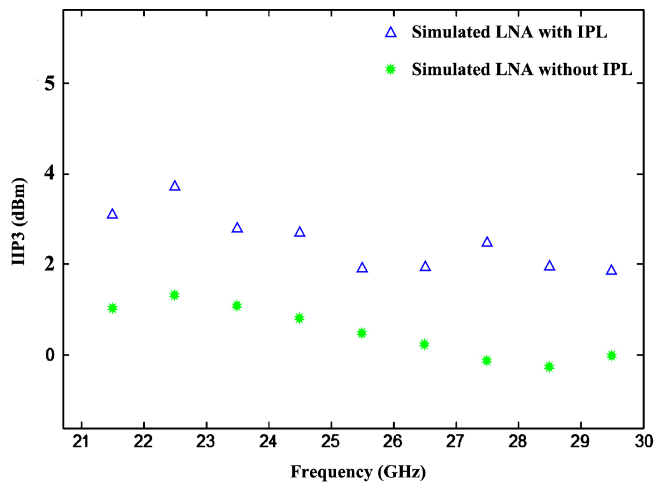
The third-order non-linearity of the Iout (third term in (Equation (26))) should be zero or close to zero in order to attain a better IIP3. The IPL technique uses voltage V2 and duplicates the non-linear drain current of transistor M2, partially canceling both second-order and third-order distortion terms. Finally, M2, Mn, and Mp use the same finger sizes to improve matching and, hence, the cancellation of harmonics. The relationship between the M2 source voltage V1, M2 drain voltage V2, and the input voltage Vin at the gate of transistor M2 can be stated up to the third order in Equation (27), while the expression of IIP3 is calculated as shown in Equation (28):
V 1 = A 1 ω o V i n + A 2 ω 1 ω 2 o V i n 2 + C 3 ω 1 , ω 2 , ω 3 , o V i n 3
I I P 3 = 20 . l o g 10 | 4 3 . C 1 ω C 3 ω 1 , ω 2 , ω 3 + 10 dB
where “o” is the Volterra series operator [35]. C1( ω ) is usually fixed by the design parameters; therefore, low distortion is achieved by reducing C3( ω 1, ω 2, ω 3). The MOS transistor operated in saturation region exhibits third-order negative transconductance and second-order positive transconductance, so concurrently decreasing the second- and third-order transconductance increases IIP3. The simulated results of IIP3 vs. frequency with and without implemented IPL are shown in Figure 10.
Figure 11 depicts that the flowchart of the proposed LNA using the an-QNA algorithm begins with the design process initiation, where the optimized LNA circuit is developed using the an-QNA method. The first step is selecting the 65 nm CMOS technology, which serves as the basis for the LNA fabrication. Next, the single-ended-to-differential two-stage LNA circuit block is designed, establishing the core structure. Transistor devices and lumped components, such as resistors and capacitors, are then sized according to the performance needs. The an-QNA algorithm is applied to optimize key parameters like gain, NF, and output power, with modifications to guarantee global convergence through quadratic estimation. The performance of the LNA is subsequently evaluated, and if the specifications (such as gain, NF, and linearity) are met, then the design moves forward. If not, further optimization is performed. Finally, once all performance criteria are satisfied, the optimal values for the transistors and components are finalized, completing the design process of the LNA using the an-QNA method.

4. Results and Discussion

An LNA based on the proposed design is simulated on CMOS with 65 nm. The proposed an-QNA-based optimized LNA consumes 28 mW of power and operates at 1.8 volts.
Figure 12 presents the simulated gain S21 of the proposed LNA (using an-QNA c-QN and, w/o optimization). In an-QNA, the simulated gain S21 is 17.5 dB, while in c-QN, it is 15 dB. A 13.9 dB simulated gain S21 without optimization is also achieved.
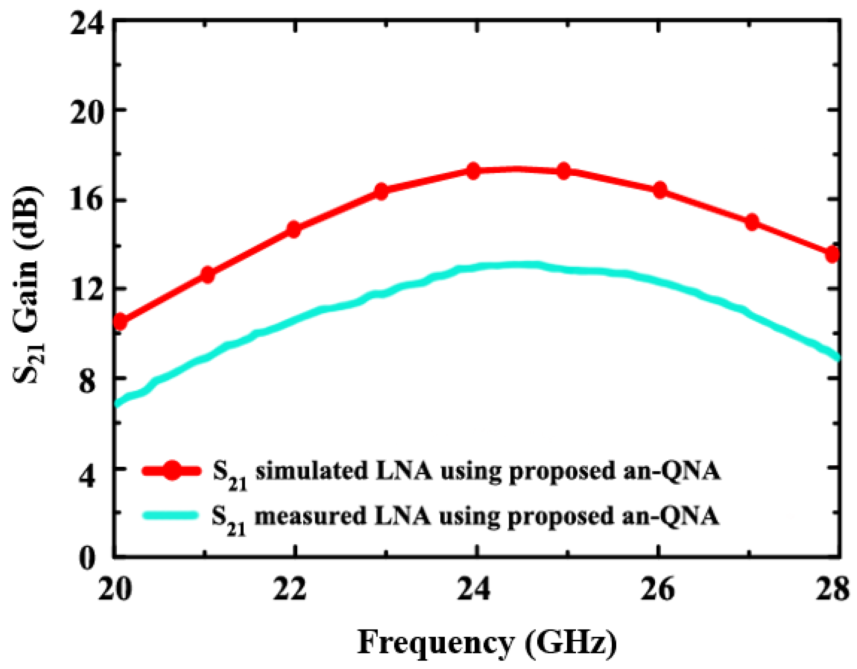
In Figure 13, the simulated and measured gain S21 of the proposed LNA (using an-QNA) is shown. According to the simulation, the measured one is 12.9 dB, while the simulated one is 17.5 dB.
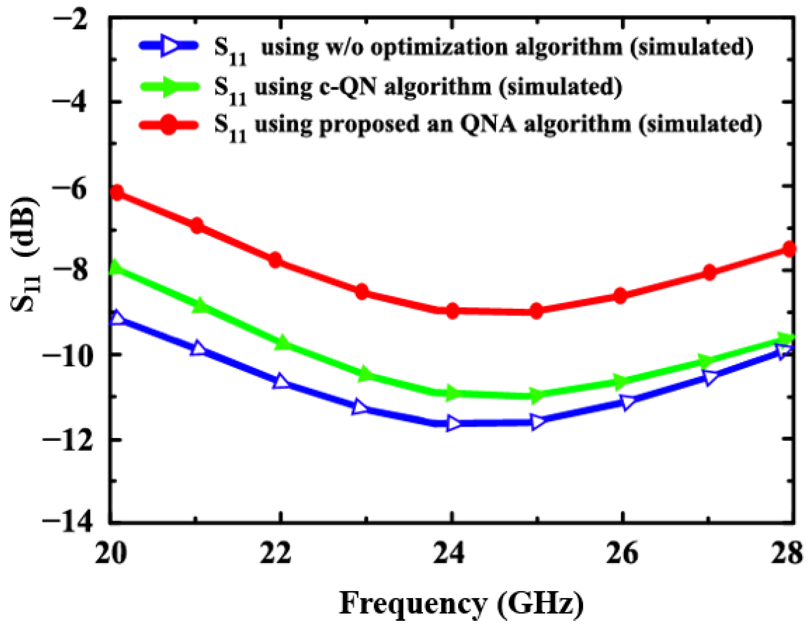
In Figure 14 and Figure 15, the simulated S22 and S11 for the proposed LNA (using an-QNA and c-QN and without optimization) is illustrated. The S11 simulation results are −9.1 dB, −10.9 dB, and −11.7 dB, and those for S22 (an-QNA and c-QN without optimization) are −8 dB, −9.8 dB, and −10.2 dB, respectively.
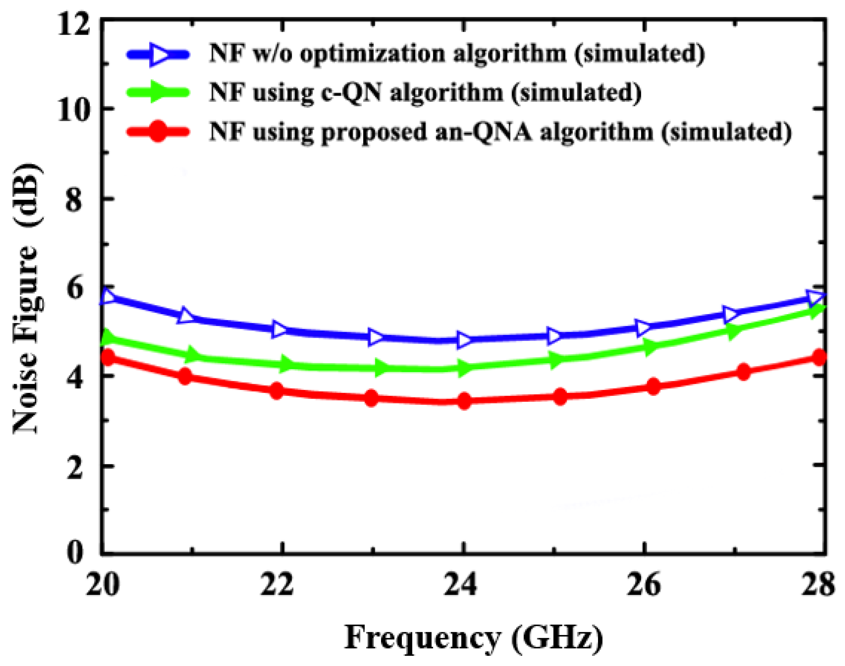
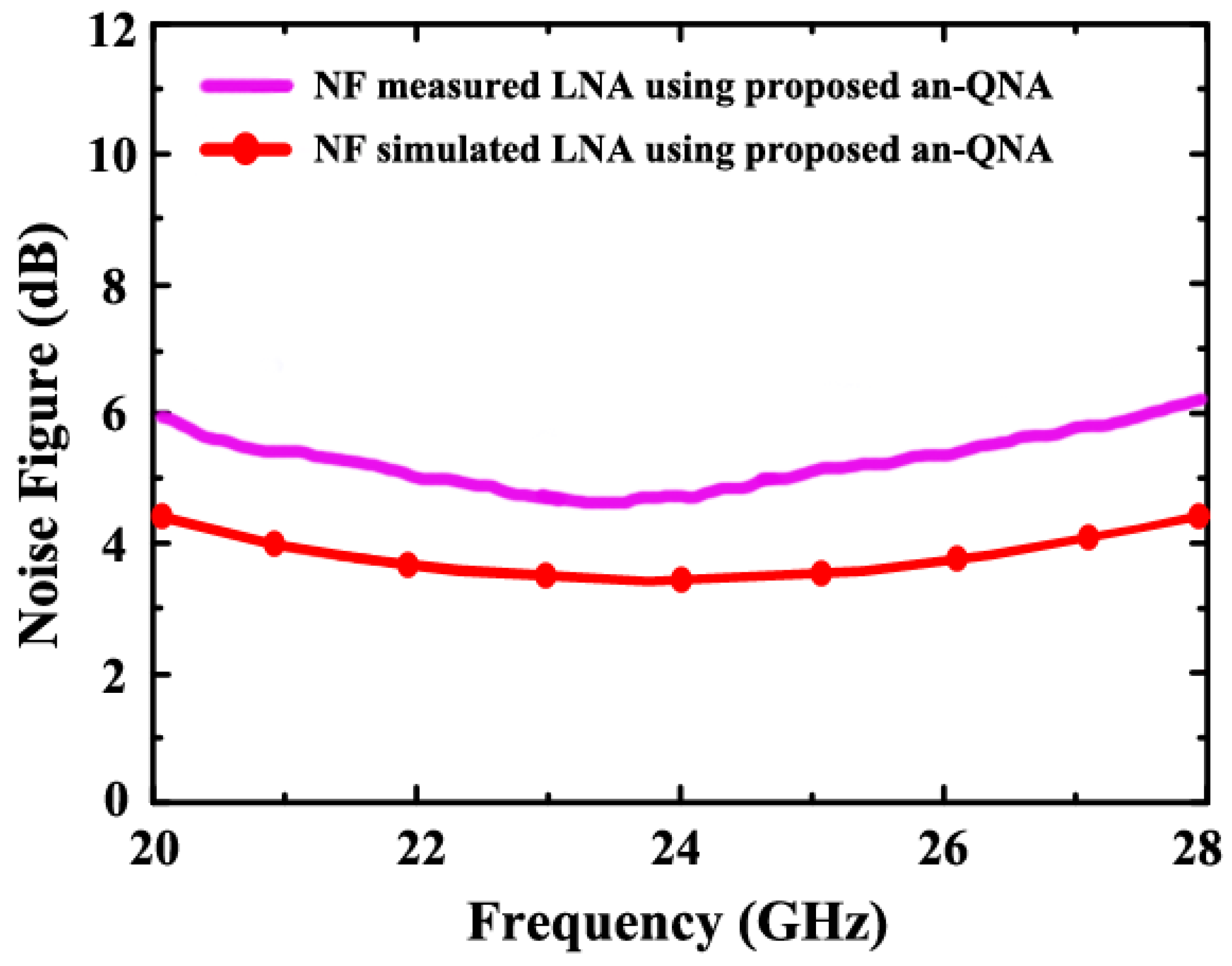
Figure 16 and Figure 17 demonstrate the simulated NF and measured NF of the proposed LNA (using an-QNA and c-QN and without optimization). The simulated NF is 3.7 dB, but the measured NF is 4.98 dB.
Figure 18 depicts the simulated IP1dB of the proposed LNA (using an-QNA). In simulations, the IP1dB of an LNA based on a QNA is achieved at −13.1 dB.
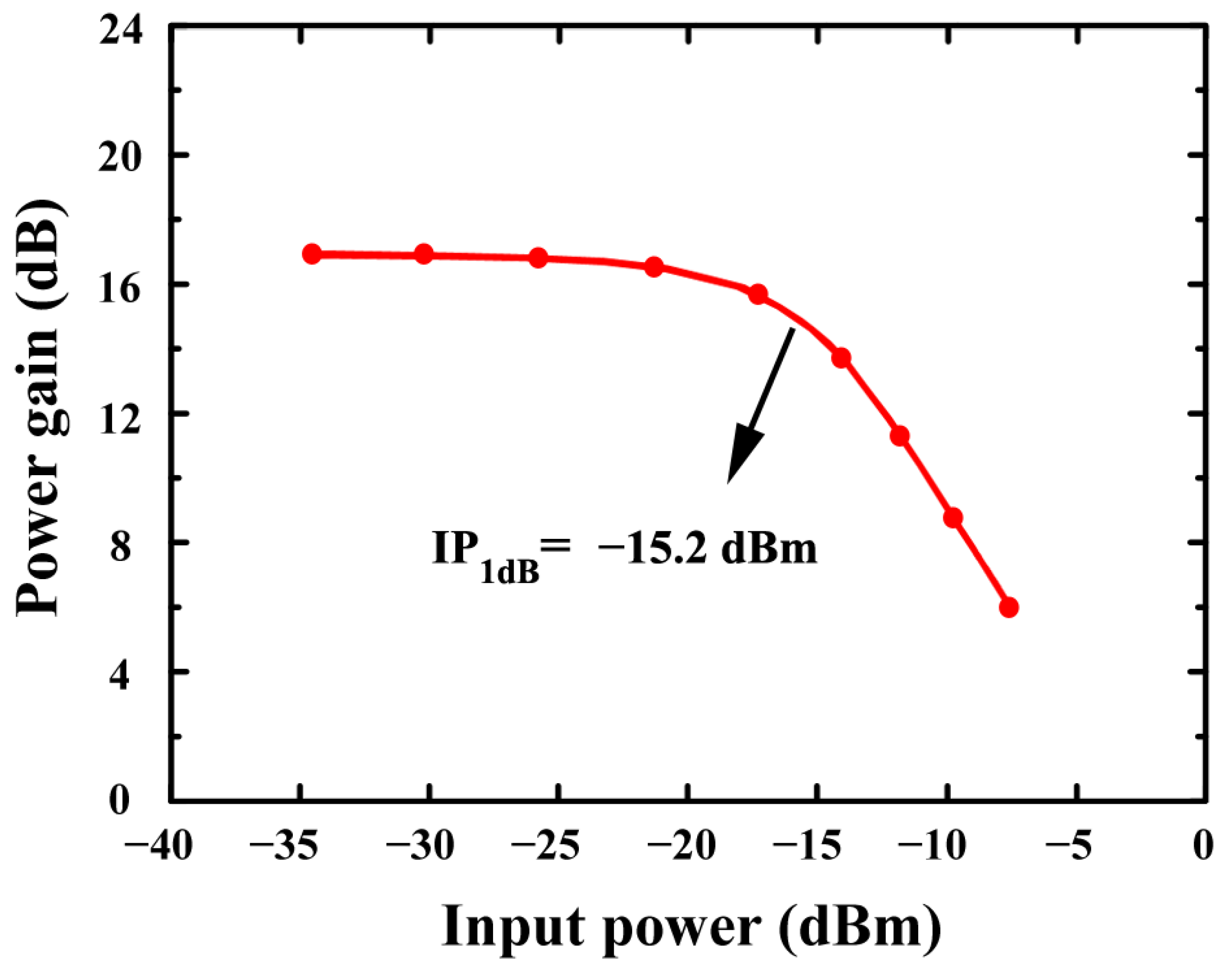
According to Figure 19, the proposed LNA’s IP1dB is simulated using c-QN. Based on simulations, an LNA using c-QN achieves −15.2 dB IP1dB.
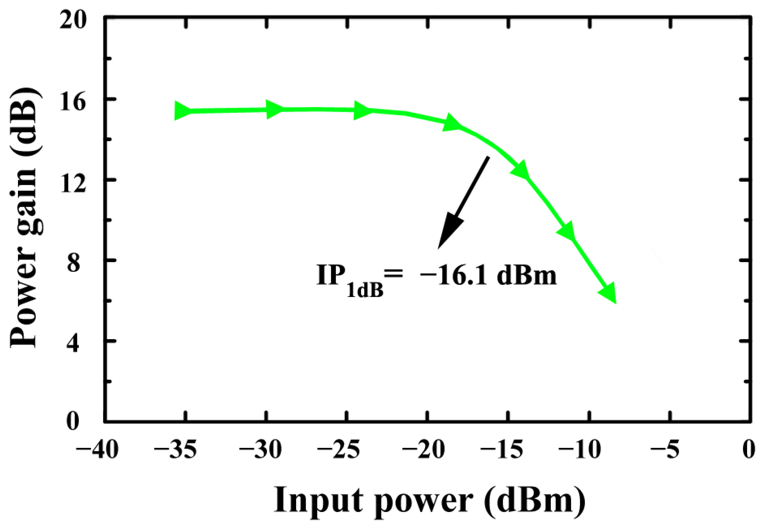
Figure 20 illustrates the simulated IP1dB of the proposed LNA (without optimization). The LNA without optimization has an IP1dB of −16.1 dB in simulations.
Figure 21 depicts the simulated and measured IP1dB of the proposed LNA (using an-QNA). In simulations, the IP1dB of an LNA based on an-QNA is −13.1 dB, while measured one is −17.5 dB.
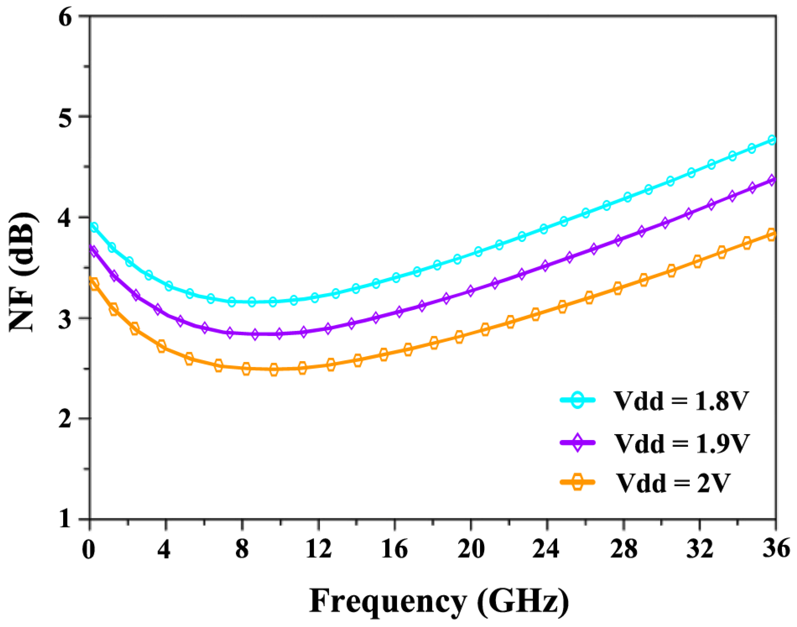
Figure 22 illustrates the NF characteristics at different supply voltages (Vdd). The NF reaches a maximum value of 3.7 dB at 24 GHz when operating at 1.8 V, while it decreases to a minimum of 3 dB when the supply voltage is increased to 2.0 V. Figure 23 shows the variation in S21 across different voltages. At 1.8 V, the S21 achieves 17.5 dB, and as the voltage increases, S21 improves further, reaching 18 dB at 1.9 V and 18.9 dB at 2.0 V.
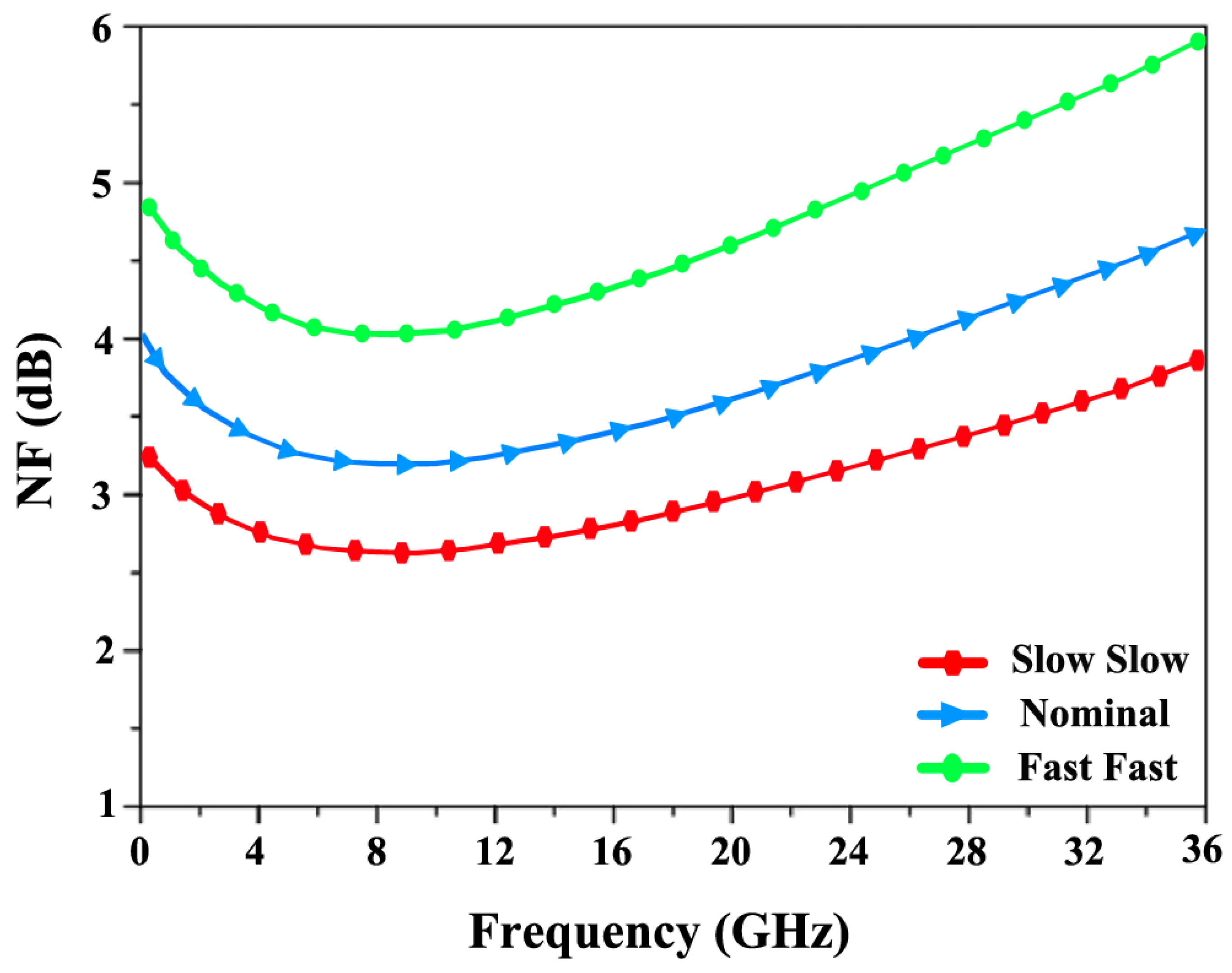
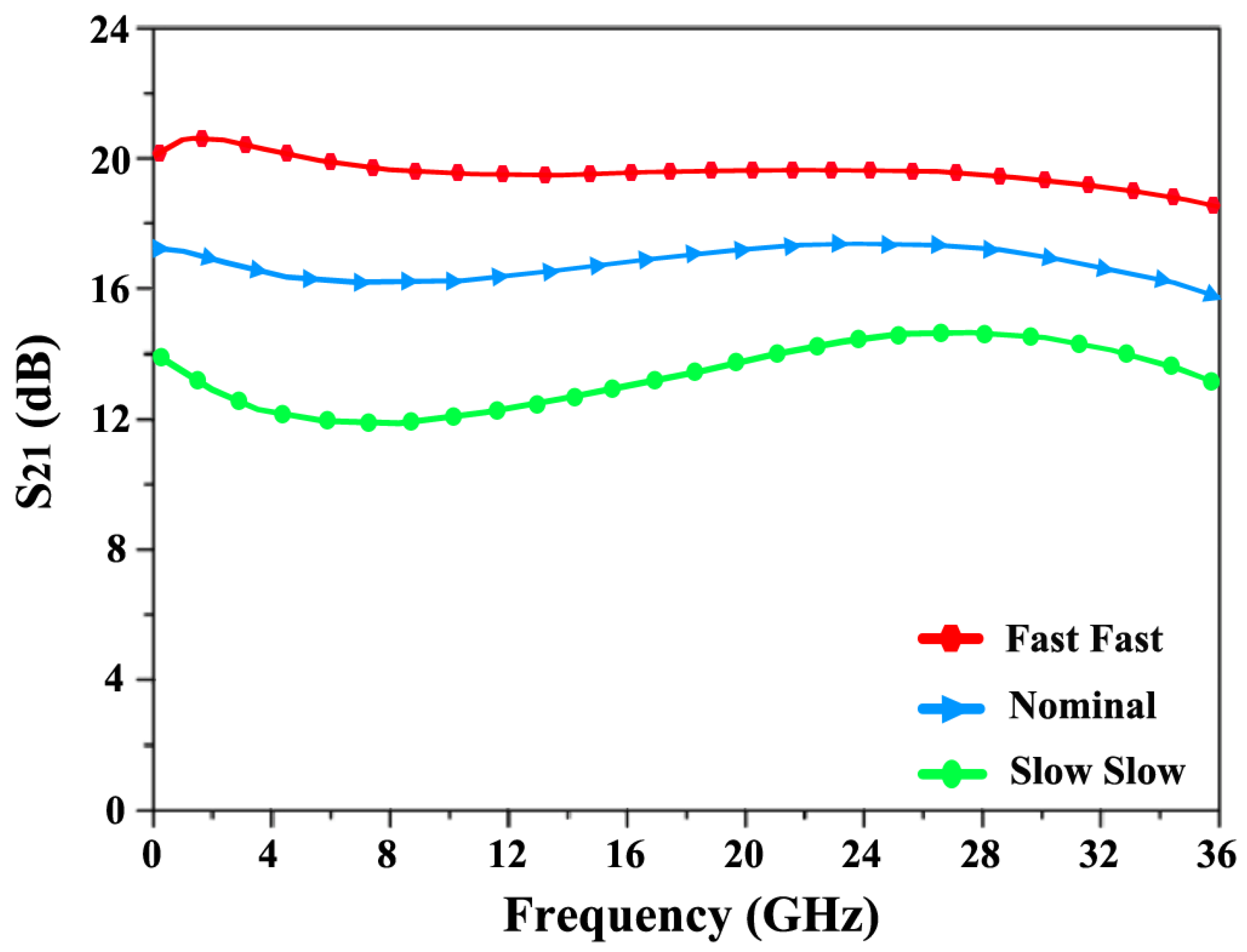
To evaluate the variations from the nominal simulation results, a linear process corner analysis was conducted at the slow–slow (SS) and fast–fast (FF) corners in Figure 24 and Figure 25. It was observed that the NF fluctuates between 4.9 dB at the FF corner and 3.1 dB at the SS corner, with a nominal value of 3.7 dB. Meanwhile, the S21 reaches a minimum of 14.2 dB at the SS corner and a maximum of 19.8 dB at the FF corner, with a nominal value of 17.5 dB.
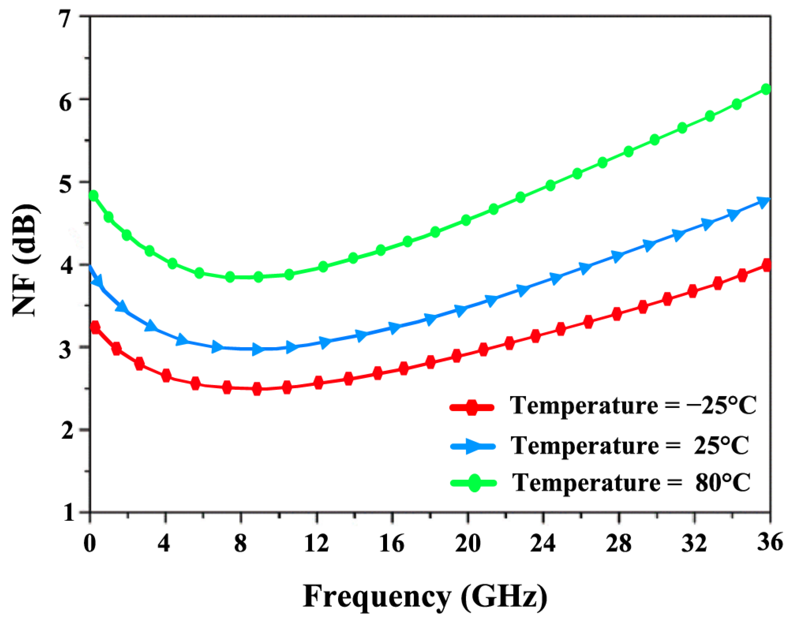
Figure 26 explores the influence of temperature fluctuations, ranging from −25 °C to 80 °C, on the NF and power gain (S21) over the frequency range of 12 to 28 GHz. As the temperature rises, the NF increases, with a minimum of 4.9 dB at 80 °C and 3.1 dB at −25 °C. Additionally, the rise in temperature causes resistive components to consume more DC power, leading to a reduction in overall power gain. Figure 27 shows that S21 decreases from a maximum of 19.8 dB at −25 °C to a minimum of 14.2 dB at 80 °C.
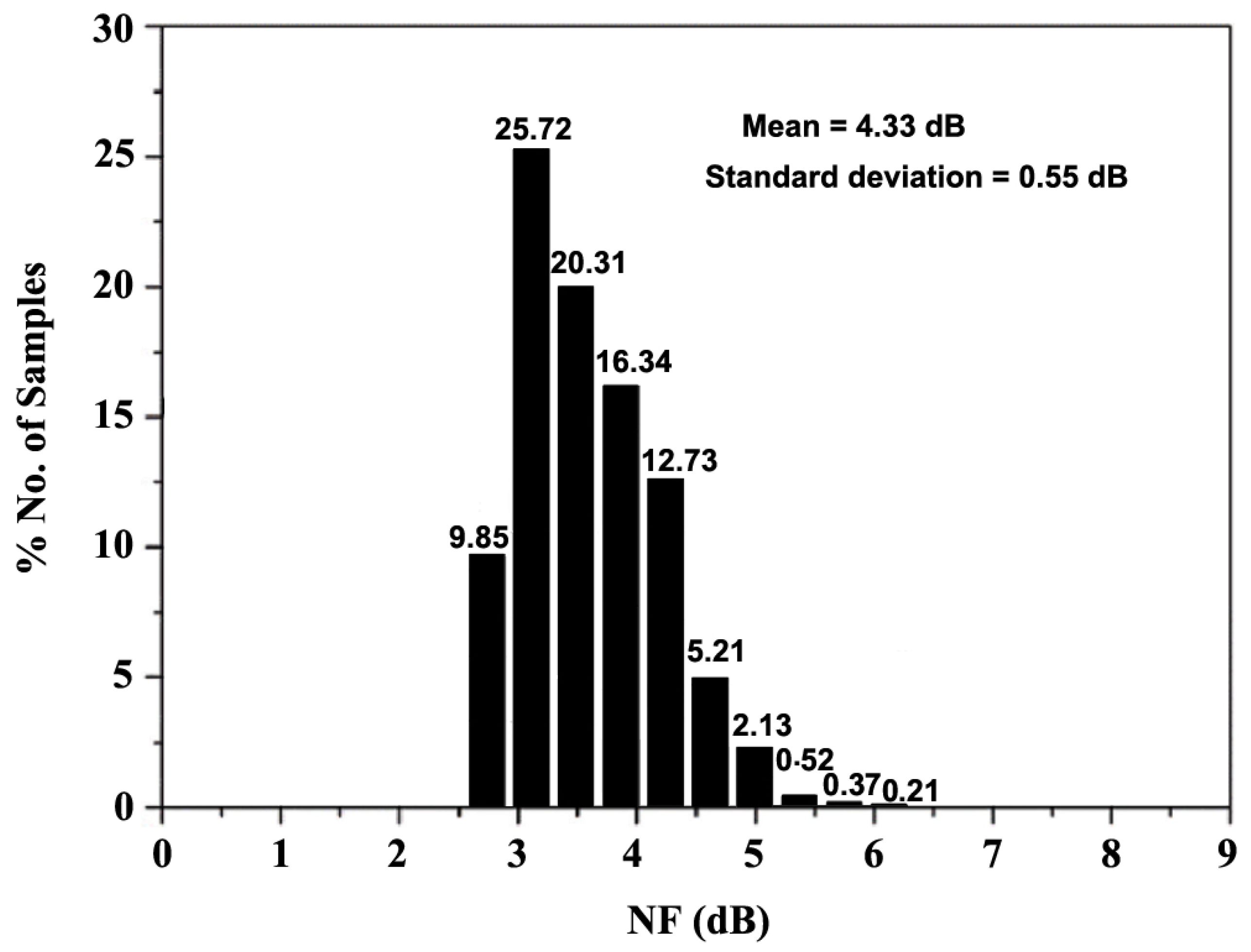
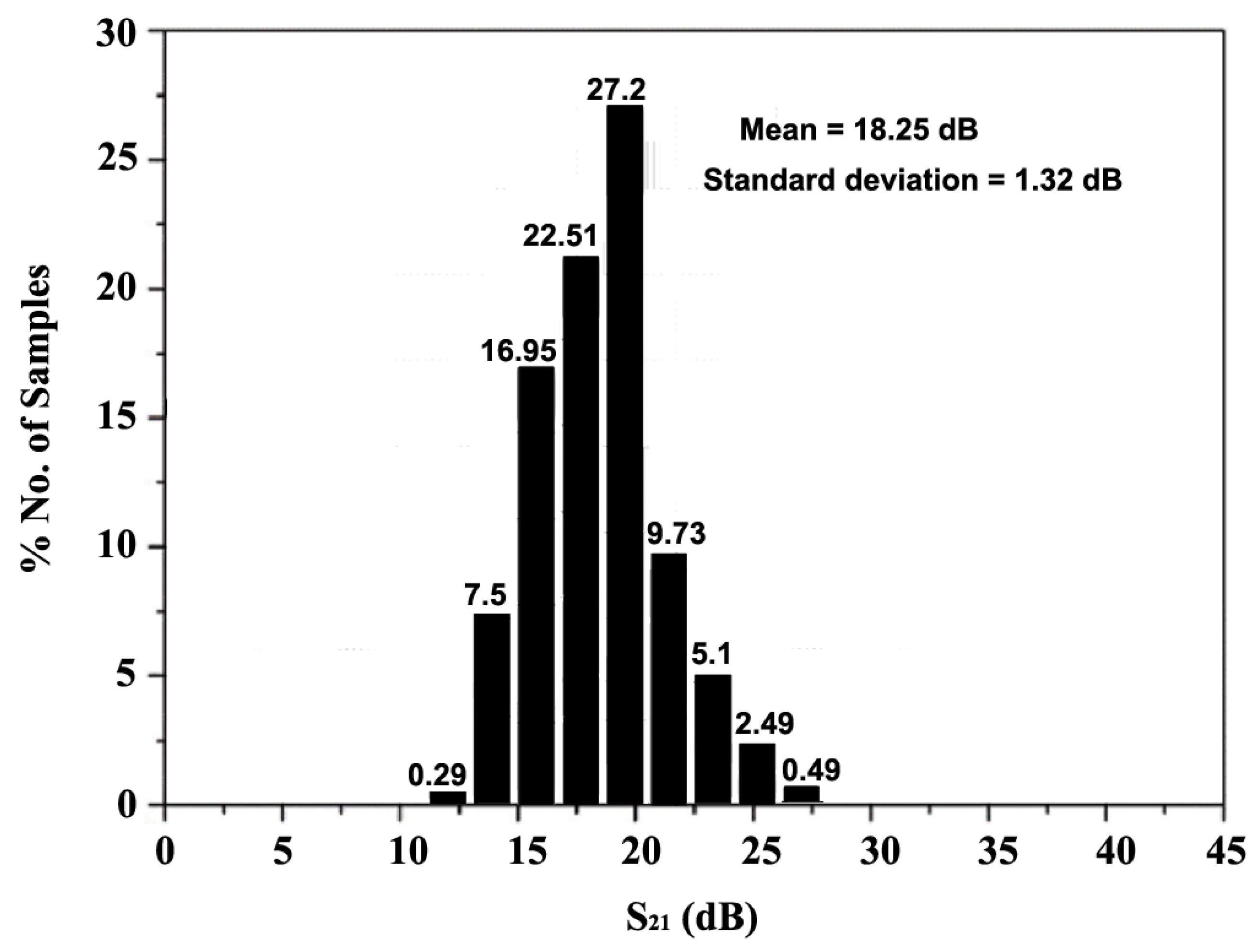
The histogram for the NF, generated after 10,000 trials in the Monte Carlo (MC) analysis, provides a statistical distribution of the NF values. This analysis allows for the observation of how NF varies across the trials, offering insights into the overall performance and consistency of the system under varying conditions. Figure 28 and Figure 29 present the MC analysis, performed to assess the variations in NF and S21, respectively. For the frequency range of 10–30 GHz, 100 iterations were conducted to evaluate the frequency response of NF and S21, while the histogram plots of NF and S21 were generated after 10,000 trial runs. The MC analysis in Figure 28 reveals that 90.5% of the samples meet the requirements, with an NF below 3.7 dB after 10,000 trials. Additionally, Figure 29 shows that the mean NF is 4.33 dB with a standard deviation of 0.55 dB. As for S21, the results in Figure 29 indicate that the mean power gain is 18.25 dB with a standard deviation of 1.32 dB after 10,000 trials.

Layout Issues

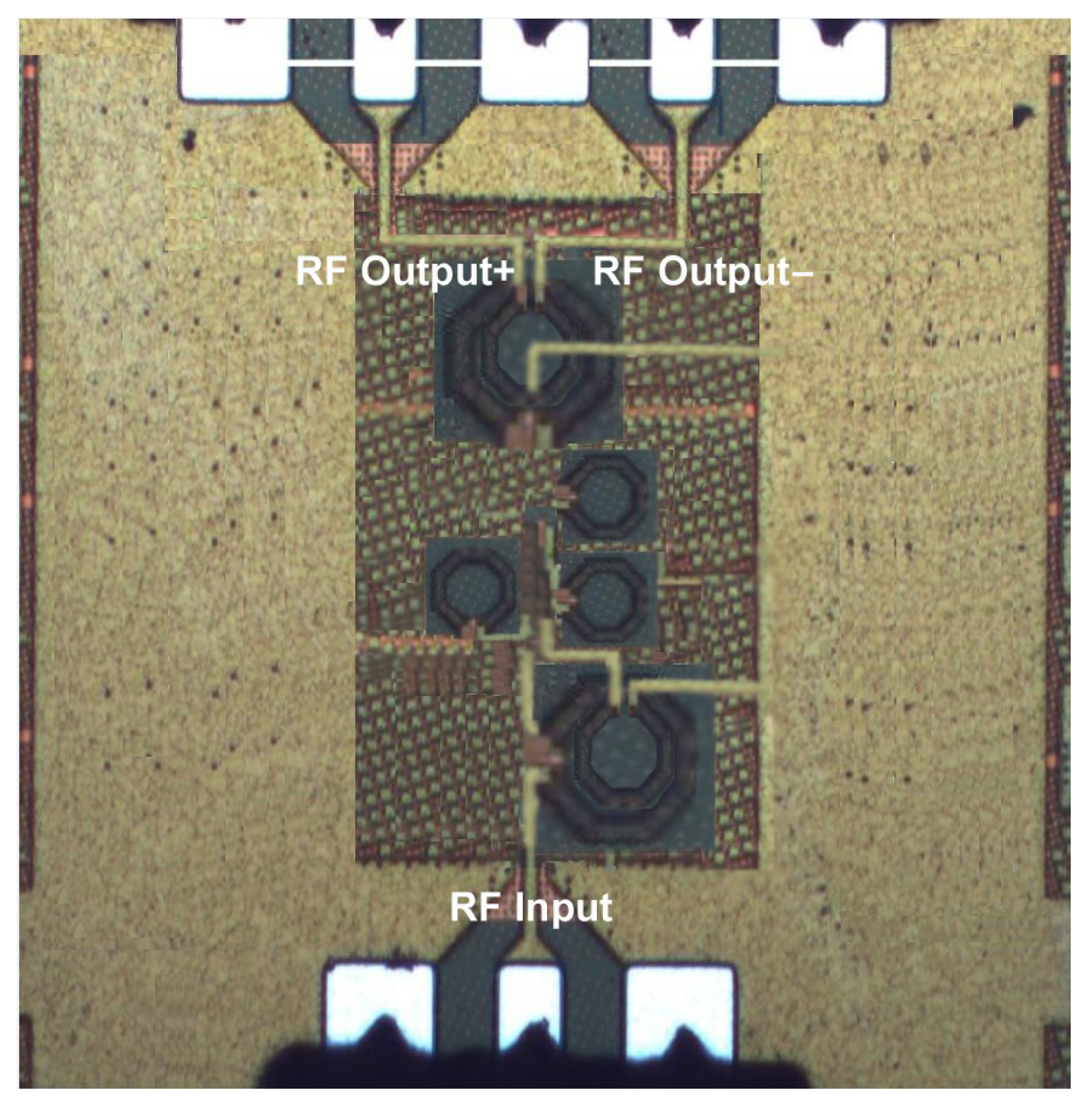
Figure 30 depicts the chip photograph of the proposed LNA. The proposed LNA has been designed and fabricated using CMOS 65 nm technology. The inductive and capacitive parasitic effects have been attempted to be minimized by carefully laid out the compact chip layout. To reduce the transistors’ series gate resistance and to avoid nonlinearity due to transistors’ parasitic shunt capacitance, the layout of LNA transistors was designed with a 2 μ m width per finger. Two fF/ μ m2 metal–insulator–metal (MIM) capacitors were used in the LNA design, and a multilayer metal structure was used to minimize the inductance and resistance of the ground plane. The top metal layer, layer 9, was used to design the inductors with a quality factor (Q) of 13 at 24 GHz, and the output transformer was designed with a metal layer 8 and metal layer 9. The designed LNA chip die size was 0.67 mm2. The Cadence Spectre RF simulator was used to calculate the post-layout results of the designed LNA. The large-signal measurement of the LNA was achieved using the Agilent spectrum analyzer (PXA N9030 A) and Agilent signal generator (PSG 8257D). Small signal measurement was conducted by using the S parameter simulation technique, and it acquired specifications of LNA, which included gain, noise value, and reflection coefficient.
In Table 11, we summarize the performance characteristics of the other reported CMOS LNAs along with the proposed LNA.

5. Conclusions and Future Research

In conclusion, an-QNA method has been developed in this paper that significantly improves the performance of LNAs. Additionally, the proposed method accelerates convergence while improving linearity using I IPL techniques and ensuring global convergence. A highly efficient LNA is designed to achieve enhanced performance using 65 nm CMOS technology, and as a result, achieves a simulated gain of 17.5 dB, an NF of 3.7 dB, as well as an (IP1dB) of −13.1 dBm. The optimized an-QNA-based LNA includes a measured gain of 12.9 dB, a measured NF of 4.98 dB, and a measured compression point of the input 1 dB of −17.8 dB. The chip area of the optimized LNA is 0.67 mm2. In automobile radar applications, these advancements demonstrate the potential of the an-QNA method. Future research could explore alternative CMOS nodes, such as 45 nm or 28 nm, that may enhance performance further. Moreover, further research is needed to optimize power consumption while maintaining performance, expand the frequency range, determine the robustness of the LNA against variations in the processing process, and integrate the LNA with other components of the radar system.

Author Contributions

Conceptualization, U.A. and T.S.D.; methodology, U.A., L.S.W. and T.S.D.; validation, U.A. and A.S.; formal analysis, A.J., U.A. and A.S.; investigation Y.L. and T.S.D.; resources, Y.L. and J.-Y.R.; data curation, A.S. and Y.L.; writing—original draft preparation, A.S. and T.S.D.; writing—review and editing, Y.L. and J.-Y.R.; supervision, A.S., Y.L. and J.-Y.R.; funding acquisition, J.-Y.R. All authors have read and agreed to the published version of this manuscript.

Funding

We are thankful to the National Research Foundation (NRF) (2018R1D1A1B07043286) of Korea for sponsoring this research publication under Project BK21 FOUR (Smart Robot Convergence and Application Education Research Center).

Institutional Review Board Statement

Not applicable.

Informed Consent Statement

Not applicable.

Data Availability Statement

Data are contained within the article.

Acknowledgments

This research was supported by the Basic Science Research Program through the *National Research Foundation of Korea* (NRF) funded by the Ministry of Education. We are also thankful to the IC Design Education Center (IDEC), Korea, for their support for chip fabrication and EDA tools.

Conflicts of Interest

The authors declare no conflicts of interest.

References

  1. As, D.E.; Yelten, M.B. A highly-linear, sub-mW LNA at 2.4 GHz in 40 nm CMOS process. Integration 2023, 88, 278–285. [Google Scholar]
  2. Lin, H.T.; Gao, L.; Li, H.Y.; Xu, J.X.; Zhang, X.Y. A 23.6–46.5 GHz LNA with 3 dB NF and 24 dB Gain Tuning Range in 28-nm CMOS Technology. IEEE Trans. Circuits Syst. I Regul. Pap. 2023, 71, 29–39. [Google Scholar] [CrossRef]
  3. Roobert, A.A.; Arunodhayamary, P.S.; Rani, D.G.N.; Venkatesh, M.; Julus, L.J. Design and analysis of 28 GHz CMOS low power LNA with 6.4 dB gain variability for 5G applications. Trans. Emerg. Telecommun. Technol. 2022, 33, e4486. [Google Scholar] [CrossRef]
  4. Kalra, D.; Srivastava, M. Design and optimization of variable gain LNA for IoT applications using meta-heuristics search algorithms. Microelectron. Eng. 2024, 286, 112125. [Google Scholar] [CrossRef]
  5. Kim, D.; Im, D. A reconfigurable balun-LNA and tunable filter with frequency-optimized harmonic rejection for sub-GHz and 2.4 GHz IoT receivers. IEEE Trans. Circuits Syst. I Regul. Pap. 2022, 69, 3164–3176. [Google Scholar] [CrossRef]
  6. Pandey, R.J.; Raghava, N.S. Harmonic analysis of CMOS low noise amplifier with employing PMOS IMD technique for biosensor applications. Microsyst. Technol. 2023, 29, 875–898. [Google Scholar] [CrossRef]
  7. Deng, Z.; Zhou, J.; Qian, H.J.; Luo, X. A 22.9–38.2-GHz dual-path noise-canceling LNA with 2.65–4.62-dB NF in 28-nm CMOS. IEEE J. Solid-State Circuits 2021, 56, 3348–3359. [Google Scholar] [CrossRef]
  8. Seifi, Z.; Ghorbani, A.; Abdipour, A. Analysis and experimental study of radiative microwave pulses ef-fects on the nonlinear performance of a low-noise amplifier. IEEE Trans. Plasma Sci. 2021, 49, 1105–1114. [Google Scholar] [CrossRef]
  9. Shen, C.; Zhao, P.; Luo, X. On energy efficient uplink multi-user mimo with shared lna con-trol. In Proceedings of the ICC 2021-IEEE International Conference on Communications, Montreal, QC, Canada, 14–23 June 2021; pp. 1–6. [Google Scholar]
  10. Ibragimov, A.M.; Mikhailov, M.N.; Smirnov, E.P. Reducing odd-order nonlinear distortions in a low noise amplifier. In Proceedings of the 2023 5th International Youth Conference on Radio Electronics, Electrical and Power Engineering (REEPE), Moscow, Russia, 16–18 March 2023; Volume 5, pp. 1–5. [Google Scholar]
  11. Younis, A.T.; Abdo, E.A. Low noise amplifier (LNA) performance optimization using genetic algorithms (GAS). J. Eng. Sci. Technol. 2020, 15, 3122–3131. [Google Scholar]
  12. Bouali, H.; Benhala, B.; Guerbaoui, M. Multi-objective optimization of CMOS low noise amplifier through nature-inspired swarm intelligence. Bull. Electr. Eng. Inform. 2023, 12, 2824–2836. [Google Scholar] [CrossRef]
  13. Dheerai, R.; Hiranmayee, K.B.; Praveena, K.S.; Dhanaraj, A.B.; Mallikarjuna, B.; Bhargavi, K. A Study on LNA, PLL and BPF of Front-End Integrated RF Receiver for Wireless Applications. In Proceedings of the 2021 6th International Conference on Communication and Electronics Systems (ICCES), Coimbatore, India, 8–10 July 2021; pp. 977–982. [Google Scholar]
  14. Kalra, D.; Goyal, V.; Srivastava, M. LNA Parameters Optimization Using Firefly Algorithm. In Proceedings of the 2023 3rd International Conference on Advancement in Electronics & Communication Engineering (AECE), Ghaziabad, India, 23–24 November 2023; pp. 94–97. [Google Scholar]
  15. Abi, S.; Bouyghf, H.; Benhala, B.; Raihani, A. An optimal design of a short-channel RF low noise amplifier using a swarm intelligence technique. In Embedded Systems and Artificial Intelligence: Proceedings of the ESAI 2019, Fez, Morocco, 6–7 November 2019; Springer: Singapore, 2019; pp. 143–153. [Google Scholar]
  16. Bouali, H.; Benhala, B.; Bouyghf, H. Optimal Design of CMOS 0.18 µm Low Noise Amplifier using Multi-Objective Artificial Bee Colony Algorithm. Int. J. Adv. Trends Comput. Sci. Eng. 2020, 9, 69–75. [Google Scholar] [CrossRef]
  17. Thakker, R.A.; Baghini, M.S.; Patil, M.B. Low-power low-voltage analog circuit design using hierarchical particle swarm optimization. In Proceedings of the IEEE 22nd International Conference on VLSI Design 2009, New Delh, India, 5–9 January 2009; pp. 427–432. [Google Scholar]
  18. Fakhfakh, M.; Cooren, Y.; Sallem, A.; Loulou, M.; Siarry, P. Analog circuit design optimization through the particle swarm optimization technique. Analog. Integr. Circuits Signal Process. 2010, 63, 71–82. [Google Scholar] [CrossRef]
  19. Tulunay, G.; Balkir, S.A. synthesis tool for CMOS RF low noise amplifiers. IEEE Trans. CAD Integr. Circuits Syst. 2008, 21, 977–982. [Google Scholar] [CrossRef]
  20. Wen, W.; Yilong, L.; Jeffrey, S.F.; Yong, Z. Particle Swarm Optimization and Finite- Element Based Approach for Microwave Filter Design. IEEE Trans. Magn. 2005, 41, 1800–1803. [Google Scholar]
  21. Sad, C.; Michailidis, A.; Noulis, T.; Siozios, K. A Hybrid GA/ML-Based End-to-End Automated Methodology for Design Acceleration of Wireless Communications CMOS LNAs. Electronics 2023, 12, 2428. [Google Scholar] [CrossRef]
  22. Liao, T.; Zhang, L. Efficient parasitic-aware hybrid sizing methodology for analog and RF integrated circuits. Integration 2018, 62, 301–313. [Google Scholar] [CrossRef]
  23. Olenšek, J.; Bűrmen, Á.; Puhan, J.; Tuma, T. DESA: A new hybrid global optimization method and its application to analog integrated circuit sizing. J. Glob. Optim. 2009, 44, 53–77. [Google Scholar] [CrossRef]
  24. Li, Y. A simulation-based evolutionary approach to LNA circuit design optimization. Appl. Math. Comput. 2009, 209, 57–67. [Google Scholar] [CrossRef]
  25. Karkhanehchia, M.M.; Naderib, S.; Jafaria, F.; Majidifarc, S. Design and optimization of a very low noise amplifier using particle swarm optimization technique. Int. J. Eng. Technol. 2014, 2, 122–131. [Google Scholar]
  26. Shin, L.W.; Chin, N.S.; Marzuki, A. 5 GHz MMIC LNA design using particle swarm optimization. Inf. Manag. Bus. Rev. 2013, 5, 257–262. [Google Scholar]
  27. Papadimitriou, A.; Bucher, M. Multi-objective low-noise amplifier optimization using analytical model and genetic computation. Circuits Syst. Signal Process. 2017, 36, 4963–4993. [Google Scholar] [CrossRef]
  28. Khong, S.Z.; Nešić, D.; Manzie, C.; Tan, Y. Multidimensional global extremum seeking via the DIRECT optimisation algorithm. Automatica 2013, 49, 1970–1978. [Google Scholar] [CrossRef]
  29. Shams, M.; Rashedi, E.; Hakimi, A. Clustered-gravitational search algorithm and its application in parameter optimization of a low noise amplifier. Appl. Math. Comput. 2015, 258, 436–453. [Google Scholar] [CrossRef]
  30. Konstantopoulos, G.; Papathanasiou, K.; Samelis, A. Optimization of RF circuits by expert monitored genetic computation. In Proceedings of the IEEE International Symposium on Circuits and Systems (ISCAS), Island of Kos, Greece, 21–24 May 2006; pp. 5247–5250. [Google Scholar]
  31. Chen, H.-H.; Chen, M.-H.; Tsai, C.-Y. Optimization of low noise amplifier designs by genetic algorithms. In Proceedings of the International Symposium on Electromagnetic Theory (EMTS), Hiroshima, Japan, 20–23 May 2013; pp. 493–496. [Google Scholar]
  32. Dutta, A.; Dasgupta, K.; Bhattacharyya, T.K. Compact small signal modeling and PSO-based input matching of a packaged CMOS LNA in subthreshold region. Microelectron. J. 2007, 38, 1050–1056. [Google Scholar] [CrossRef]
  33. Jiang, Z.; Liu, Z.; Liu, H.; Zhao, C.; Wu, Y.; Kang, K. A 24 GHz enhanced neutralized cascode LNA with 4.7 dB NF and 19.8 dB gain. IEICE Electron. Express 2018, 15, 20180464. [Google Scholar] [CrossRef]
  34. Suganthi, K.; Malarvizhi, S. Millimeter wave CMOS minimum noise amplifier for automotive radars in the frequency band (60–66 GHZ). Clust. Comput. 2019, 22 (Suppl. 5), 11755–11764. [Google Scholar] [CrossRef]
  35. Zhang, H.; Sánchez-Sinencio, E. Linearization techniques for CMOS low noise amplifiers: A tutorial. IEEE Trans. Circuits Syst. I Regul. Pap. 2010, 58, 22–36. [Google Scholar] [CrossRef]
  36. Fan, X.; Sánchez-Sinencio, E.; Silva-Martinez, J. A 3 GHz–10 GHz common gate ultrawideband low noise amplifier. In Proceedings of the IEEE Midwest Symposium Circuits and Systems, Cincinnati, OH, USA, 7–10 August 2005; pp. 631–634. [Google Scholar]
  37. Shin, S.; Tsai, M.; Liu, R.; Lin, K.; Wang, H. A 24-GHz 3.9-dB NF low-noise amplifier using 0.18 CMOS technology. IEEE Microw. Wireless Compon. Lett. 2005, 15, 448–450. [Google Scholar] [CrossRef]
  38. Chen, Z.; Gao, H.; Leenaerts, D.; Milosevic, D.; Baltus, P. A 29–37 GHz BiCMOS low-noise amplifier with 28.5 dB peak gain and 3.1–4.1 dB NF. In Proceedings of the 2018 IEEE Radio Frequency Integrated Circuits Symposium (RFIC), Philadelphia, PA, USA, 10–12 June 2018; IEEE: Piscataway, NJ, USA, 2018; pp. 288–291. [Google Scholar]
  39. Hosseini, S.A.; Taheri, M.M.; Khosravi, R.; Moradi, G. A 27–31 GHz CMOS LNA for 5G Application via Improved Noise Cancellation Technique and Gain Boosting. Int. J. Smart Electr. Eng. 2022, 11, 21–26. [Google Scholar]
  40. Kumar, M.; Deolia, V.K. Performance analysis of low power LNA using particle swarm optimization for wide band application. AEU-Int. J. Electron. Commun. 2019, 111, 152897. [Google Scholar] [CrossRef]
  41. Kumar, R.; Talukdar, F.A.; Rajan, A.; Devi, A.; Raja, R. Parameter optimization of 5.5 GHz low noise amplifier using multi-objective Firefly Algorithm. Microsyst. Technol. 2020, 26, 3289–3297. [Google Scholar] [CrossRef]
Figure 1. Overview of RF transceiver.
Sensors 24 06141 g001
Figure 2. A 24 GHz automotive radar application.
Sensors 24 06141 g002
Figure 3. The training error vs. iteration counts of LNA.
Sensors 24 06141 g003
Figure 4. The training error vs. time of LNA.
Sensors 24 06141 g004
Figure 5. Convergence graphs of c-QN, ADAM, an-QNA algorithms (a) 1000 dimension (b) 2000 dimension (c) 3000 dimension (d) 4000 dimension (e) 5000 dimension.
Sensors 24 06141 g005
Figure 6. Convergence graph of unimodal benchmark functions (a) Fv1 (b) Fv2 (c) Fv3 (d) Fv4.
Sensors 24 06141 g006
Figure 7. Convergence graph of multimodal benchmark functions (a) Fv5 (b) Fv6 (c) Fv7 (d) Fv8.
Sensors 24 06141 g007
Figure 8. Proposed two-stage LNA using an-QNA.
Sensors 24 06141 g008
Figure 9. NFmin vs. current density.
Sensors 24 06141 g009
Figure 10. IIP3 vs. frequency.
Sensors 24 06141 g010
Figure 11. Flowchart of the proposed LNA using an-QNA.
Sensors 24 06141 g011
Figure 12. The simulated gain S21 of the proposed LNA (using an-QNA and c-QN and without optimization).
Sensors 24 06141 g012
Figure 13. The simulated and measured gain S21 of the proposed LNA (using an-QNA).
Sensors 24 06141 g013
Figure 14. The simulated S22 of the proposed LNA (using an-QNA c-QN and, w/o optimization).
Sensors 24 06141 g014
Figure 15. The simulated S11 of the proposed LNA (using an-QNA c-QN and, w/o optimization).
Sensors 24 06141 g015
Figure 16. The simulated NF of the proposed LNA (using an-QNA and c-QN and without optimization).
Sensors 24 06141 g016
Figure 17. The simulated and measured NF (using an-QNA).
Sensors 24 06141 g017
Figure 18. The simulated IP1dB of the proposed LNA (using an-QNA).
Sensors 24 06141 g018
Figure 19. The simulated IP1dB of the proposed LNA (using c-QN)).
Sensors 24 06141 g019
Figure 20. The simulated IP1dB of the proposed LNA (without optimization).
Sensors 24 06141 g020
Figure 21. The measured and simulated IP1dB of the proposed LNA (using an-QNA).
Sensors 24 06141 g021
Figure 22. NF’s response to power supply variations.
Sensors 24 06141 g022
Figure 23. S21’s response to power supply variations.
Sensors 24 06141 g023
Figure 24. Corners simulations of nominal, slow–slow (SS), and fast–fast (FF) for NF.
Sensors 24 06141 g024
Figure 25. Corners simulations of nominal, slow–slow (SS), and fast–fast (FF) for S21.
Sensors 24 06141 g025
Figure 26. S21’s response to temperature variations.
Sensors 24 06141 g026
Figure 27. NF’s response to temperature variations.
Sensors 24 06141 g027
Figure 28. Monte Carlo analysis of NF.
Sensors 24 06141 g028
Figure 29. Monte Carlo analysis of S21.
Sensors 24 06141 g029
Figure 30. Chip photograph.
Sensors 24 06141 g030
Table 1. Summary of the simulation results of LNA modeling.
Name of AlgorithmTrainingError Median/Ave/Best/Worst (w) (×10−3)Iteration Counts (k)Time (s)TestError Median/Ave/Best/Worst (w) (×10−3)Rate of Convergence (%)
c-QN0.75/0.76/0.62/0.9141,828950.640/0.901/0.534/2.0175%
an-QNA0.57/0.51/0.32/0.6535,561650.798/1.14/0.591/2.15100%
Table 2. Multimodal and unimodal benchmark functions (dimensions, minimum range).
Function NameDimensionRangeMinimum Function
(fmin)
Functionv1(unimodal) (y)30[−100, 100]0
Functionv2(unimodal) (y)30[−100, 100]0
Functionv3(unimodal) (y)30[−100, 100]0
Functionv4(unimodal) (y)30[−1.28, 1.28]0
Functionv5(multimodal) (y)30[−500, 500]−418.9 × 5
Functionv6(multimodal) (y)30[−32, 32]0
Functionv7(multimodal) (y)30[−5.1, 5.1]0
Functionv8(multimodal) (y)30[−600, 600]0
Table 3. The c-QN best solutions and statistical outcomes (unimodal benchmark functions).
c-QNMinimumMaximum μ α
6.16 × 10−615.8 × 104215.82.5 × 103
1.97 × 10−351.43 × 10121.43 × 1094.52 × 1010
3.3 × 10−151.8876 × 1051.7745 × 1031.0505 × 104
2.6647 × 10−1489.072.6112.13
27.112.1621 × 1087.4518 × 1051.0897 × 107
1.25476.5240 × 104335.93.4849 × 103
3.61 × 10−492.210.495.80
Table 4. The ADAM best solutions and statistical outcomes (unimodal benchmark functions).
ADAMMinimumMaximum μ α
2.71 × 10−736.15 × 104173.17162.53 × 103
7.42 × 10−433.2669 × 1093.2708 × 1061.03 × 108
2.52 × 10−251.1651 × 105674.73615.80 × 103
2.42 × 10−2088.030.9456.765
27.162.30 × 1086.71 × 1059.98 × 106
1.257.07 × 104197.702.81 × 103
5.791 × 10−480.650.1332.668
Table 5. The an-QNA best solutions and statistical outcomes (unimodal benchmark functions).
an-QNAMinimumMaximum μ α
0.007.10 × 104125.52.4 × 103
1.60 × 10−1753.78 × 10131.27 × 10101.1956 × 1012
1.2 × 10−2826.174 × 1041.2536 × 1031.0787 × 104
1.7 × 10−15288.030.3494.369
27.102.30 × 1083.5409 × 1051.00 × 107
3.877.07 × 104123.812.5129 × 103
1.41 × 10−580.6520.2024.97
Table 6. The c-QN best solutions and statistical outcomes (multimodal benchmark functions).
c-QNMinimumMaximum μ α
−5.80 × 10³−2.44 × 10³−4.03 × 103967.79
5.68 × 10−14458.7810.7848.011
1.50 × 10−1420.76230.4122.276
0.009665.773.14932.93
0.035.520 × 1081.57 × 1062.49 × 107
0.698.056 × 1083.20 × 1064.36 × 107
Table 7. The ADAM best solutions and statistical outcomes (multimodal benchmark functions).
ADAMMinimumMaximum μ α
−4.8344 × 10³−2.5399 × 10³−3.3352 × 103731.9012
0438.11484.946532.6783
1.5099 × 10−1420.76230.24971.7307
0527.34621.417420.4885
0.05386.1414 × 1081.1003 × 1062.1982 × 107
1.112849.0172 × 1081.5261 × 1063.2837 × 107
Table 8. The an-QNA best solutions and statistical outcomes (multimodal benchmark functions).
an-QNAMinimumMaximum μ α
−2.25 × 10³−2.23 × 10³−2.25 × 1036.3372
0488.072.3326.43
1.4 × 10−1520.84720.10451.1726
0555.030.95918.93
0.5588.105 × 1081.04 × 1062.15 × 107
0.1939.23 × 1081.103 × 1062.9672 × 107
Table 9. Proposed LNA device component values using an-QNA.
ElementDimension
M132 µm/65 nm
M254 µm/65 nm
M354 µm/65 nm
C1, C2, C31 pF, 4.2 pF, 1.2 pF
L1∼L31.3 nH, 1.5 nH, 170 pH
L4∼L61.5 nH, 1.8 nH, 154 pH
Table 10. An description of distortion sources and linearization methods [33].
Distortion
Sources
gmgds
Methods of
Linearization
Intrinsic
2nd Order
Intrinsic
3rd Order
2nd-Order
Interaction
Higher
Order
Feedback
Harmonic
termination
Optimal biasing
Feedforward
Derivative
superposition (DS)
Complementary DS
Differential DS
Modified DS
IM2 injection
Noise/distortion
cancellation
Post-Distortion
Table 11. Performance characteristics of other reported CMOS LNAs.
Ref.Tech (nm)VDD (V)FrEquation (GHz)S21 (dB)NF (dB)IP1dBPower (mW)
[36]65 nm1.56011.2891.819N/A7.25
[37]180 nmN/A2412.83.3N/A8
[38]0.25 μ m BiCMOS1.816–4310.52.5-41.8 (IIP3)24
[39]0.13 μ m CMOS1227–3122.141.86−16 (IIP3)33.4
[40]45 nmN/A5.0–27.518.57 (PSO)2.4–3.1N/A1.6
[41]180 nm1.85.522.15 (firefly)1.16−2.60 (IIP3)N/A
[This Work]65 nm1.82417.5/12.9 (sim./meas) (an-QNA)3.7/4.98 (sim./meas) (an-QNA)−13.1/−17.8 (sim./meas) (an-QNA)28
Disclaimer/Publisher’s Note: The statements, opinions and data contained in all publications are solely those of the individual author(s) and contributor(s) and not of MDPI and/or the editor(s). MDPI and/or the editor(s) disclaim responsibility for any injury to people or property resulting from any ideas, methods, instructions or products referred to in the content.