1. Introduction
Capacitive touch screen panels (TSP) have been widely used for mobile devices. There are two types of capacitive touch sensing; mutual capacitance sensing (MCS) and self-capacitance sensing (SCS) [
1]. Since MCS and SCS react differently to touch or water droplets, SCS has been utilized to correctly distinguish the actual touch and water droplets on display [
2,
3].
To provide a better form factor for mobile devices, TSP has become thinner these days. As a result, the base self-capacitance of organic light emitting diode (OLED) TSP increased by up to several hundred pF [
4,
5], and it becomes a design challenge for the SCS system. For the SCS system adopting a single-ended receiver (RX) circuit, the base capacitance occupies a large portion of the dynamic range of the analog front-end (AFE). Therefore, it requires offset compensation circuits to remove the effect of the base self-capacitance and maximize the gain for sensing the self-capacitance variation by touch [
5]. Compared to the single-ended SCS system, the fully-differential SCS system [
6], or the charge-sharing-based SCS system [
7,
8] naturally removes the offset signal because they sense the self-capacitance difference between two adjacent TSP electrodes. However, because of the self-capacitance mismatch between electrode channels, both the fully-differential- and charge-sharing-based SCS systems still suffer from dynamic range degradation.
We can briefly evaluate this sensing difficulty that arises from the large base self-capacitance and its mismatch with the electrical parameters for our design target TSP, considering specific details are withheld due to the confidentiality of the TSP manufacturer. For the RX electrodes, its base self-capacitance, , is approximately 280 , while its variation by touch, , is only about 40 . In other words, the single-ended SCS system should be able to sense around 0.014% variation of . For the fully-differential SCS system, this large base is removed naturally. However, the self-capacitance mismatch should be considered, which is caused by the TSP fabrication mismatch and the curvature on the display edge. For the RX electrode of our design target TSP, this mismatch can be up to 12%, resulting in a maximum difference. This mismatch is still 840 times larger than , even after much of the base is removed by the fully-differential operation. Thus, the self-capacitance mismatch could limit the touch system signal-to-noise ratio (SNR) or, even worse, saturate the AFE and make the SCS system unable to detect touch action.
We present the self-capacitance mismatch calibration technique for the fully-differential SCS system. By adjusting the driving strength and input resistance for each fully-differential input, the proposed system reduces the RX AFE output offset induced by the self-capacitance mismatch. Therefore, the SNR of the proposed TSP SCS system can be restored without consuming excessive power and die area.
The remainder of this paper is organized as follows:
Section 2 explains the output offset generation mechanism due to the self-capacitance mismatch.
Section 3 presents the proposed self-capacitance calibration.
Section 4 describes the implementation of the proposed TSP SCS system, including the proposed calibration.
Section 5 presents the results.
Section 6 concludes this paper.
2. Output Offset Generation Due to the Self-Capacitance Mismatch
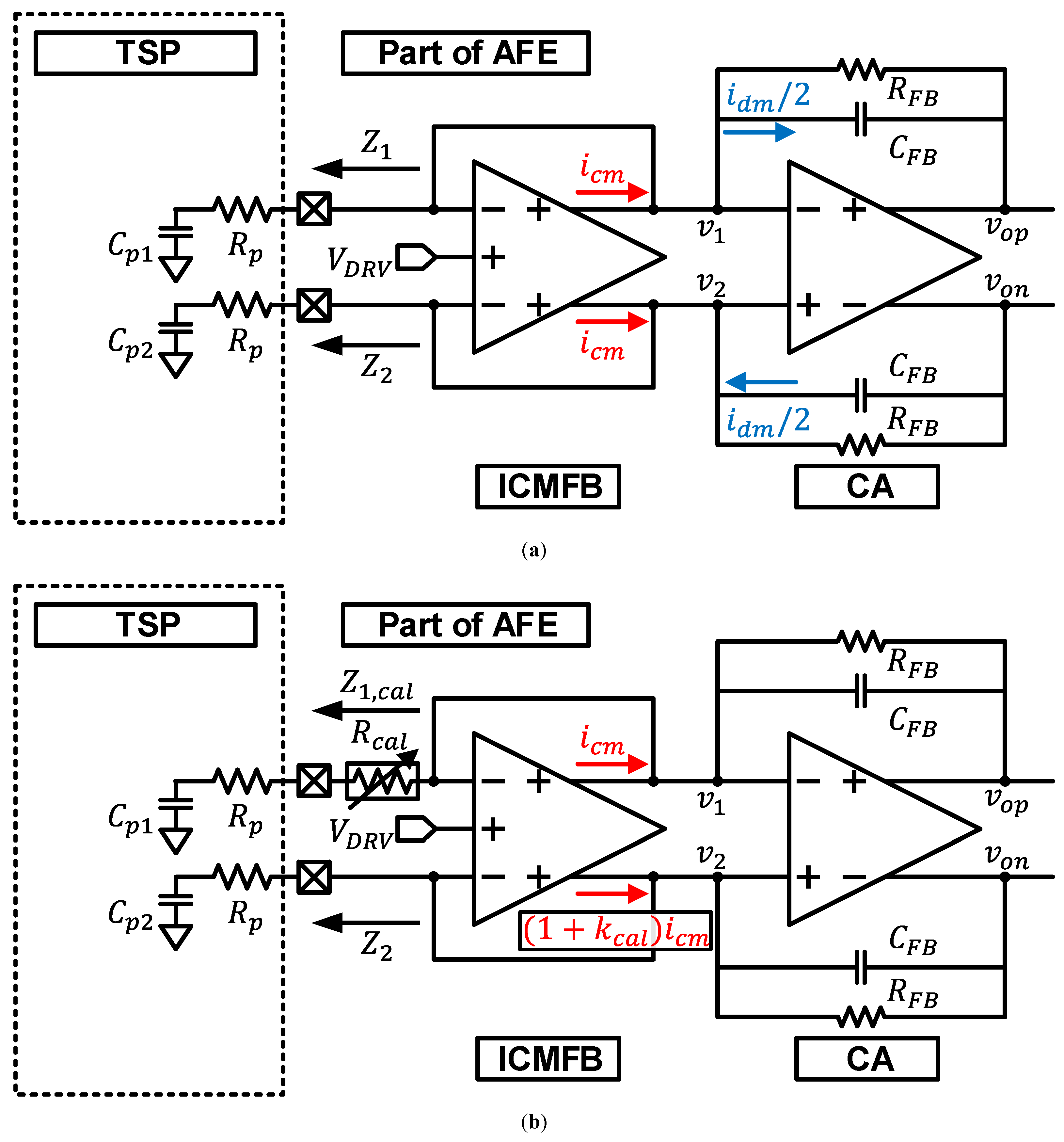
Figure 1a shows part of a fully-differential SCS system without the mismatch calibration technique. An input common-mode feedback amplifier (ICMFB) drives the self-capacitance of TSP,
and
, and the parasitic resistance,
, by the driving signal,
[
6]. Note that ICMFB can only provide a common-mode current,
. The feedback network of the AFE, which includes the ICMFB and charge amplifier (CA), tries to equalize the CA input voltages
and
in
Figure 1a. When there is no self-capacitance mismatch,
from ICMFB is sufficient to match
and
. Thus,
, which is the differential-mode current generated from CA, and its corresponding
offset is not generated, where
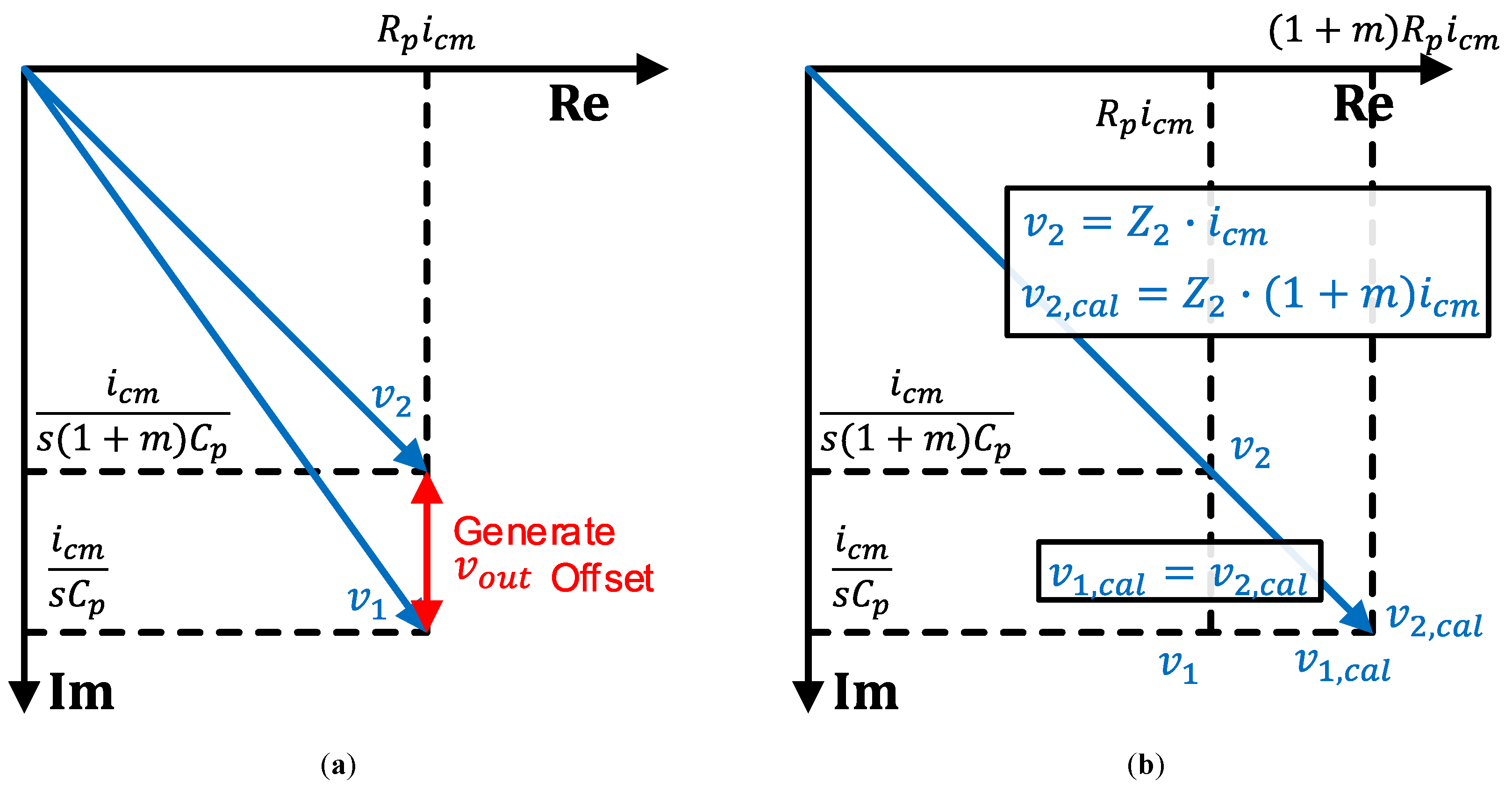
. However, if the self-capacitance mismatch exists,
alone cannot match
and
. Therefore,
from CA is generated to equalize
and
. Therefore, it becomes the output offset which degrades the dynamic range of the AFE. If we assume
and let
, where
m is self-capacitance mismatch ratio. Then,
and
is obtained as
where
and
are resistor and capacitor in the CA feedback, respectively.
An approach to suppress
generation due to the self-capacitance mismatch can be considered, which adds the extra calibration current to the
node in
Figure 1a. With this approach, the required calibration current from the external amplifier,
, is expressed as
Note that the denominator of Equation (
3) contains the Laplace variable
s, indicating that the expression involves a complex number. This implies that in order to completely remove the output offset,
must be phase-shifted relative to
. In other words, the system requires additional circuits to drive a phase-shifted signal from
, which is the self-capacitance driving signal. This leads to power and area inefficiency due to the generation of phase-shifted square or sinusoidal signals, as well as the requirement for an additional amplifier to drive the self-capacitance with a phase-shifted signal.
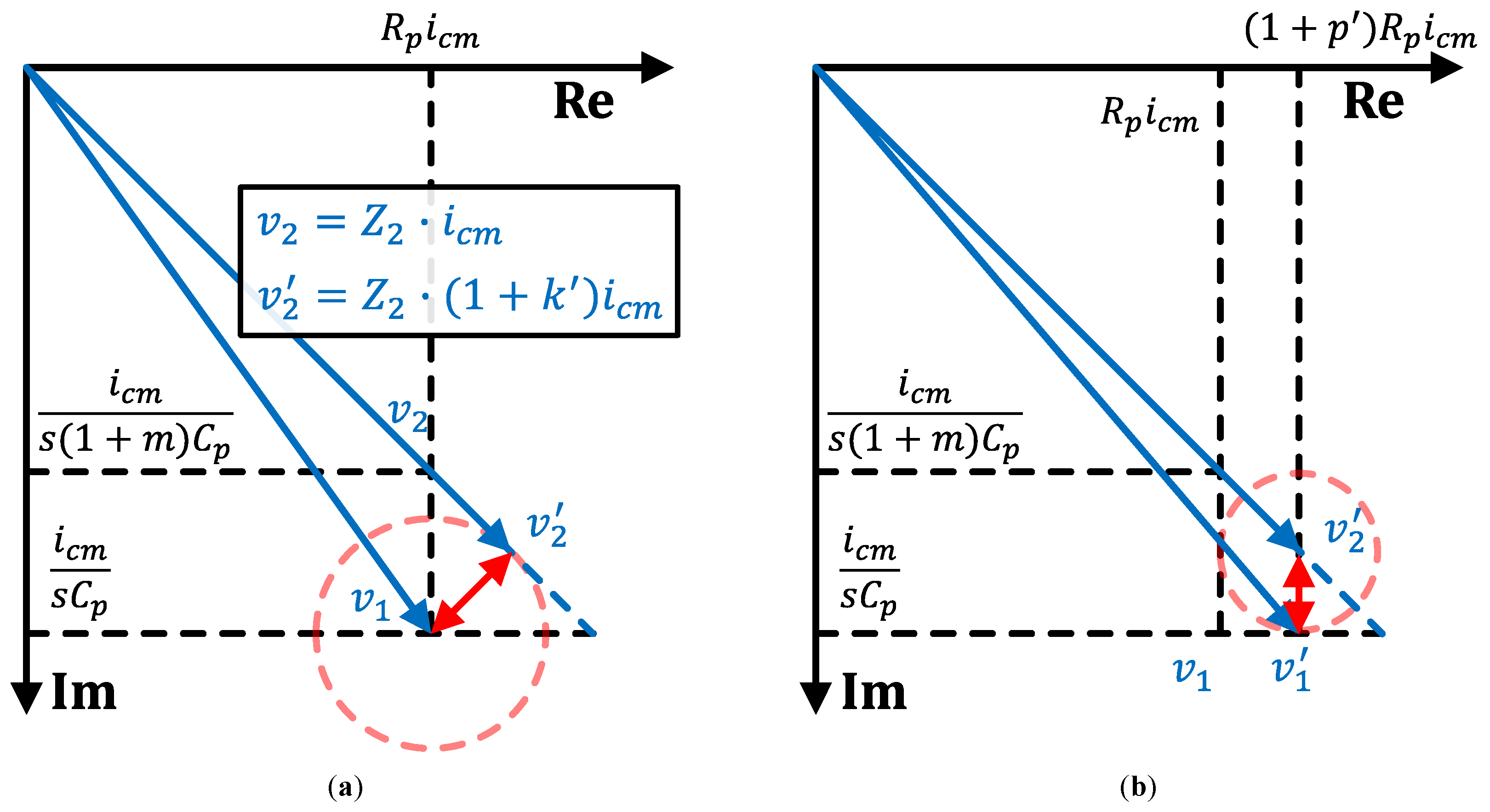
Our proposed solution is implementing programmable input resistance and ICMFB with driving strength control, as depicted in
Figure 1b. By controlling
and
, both the phase and magnitude of
and
can be matched without
generation from CA. Therefore, the
offset is minimized.
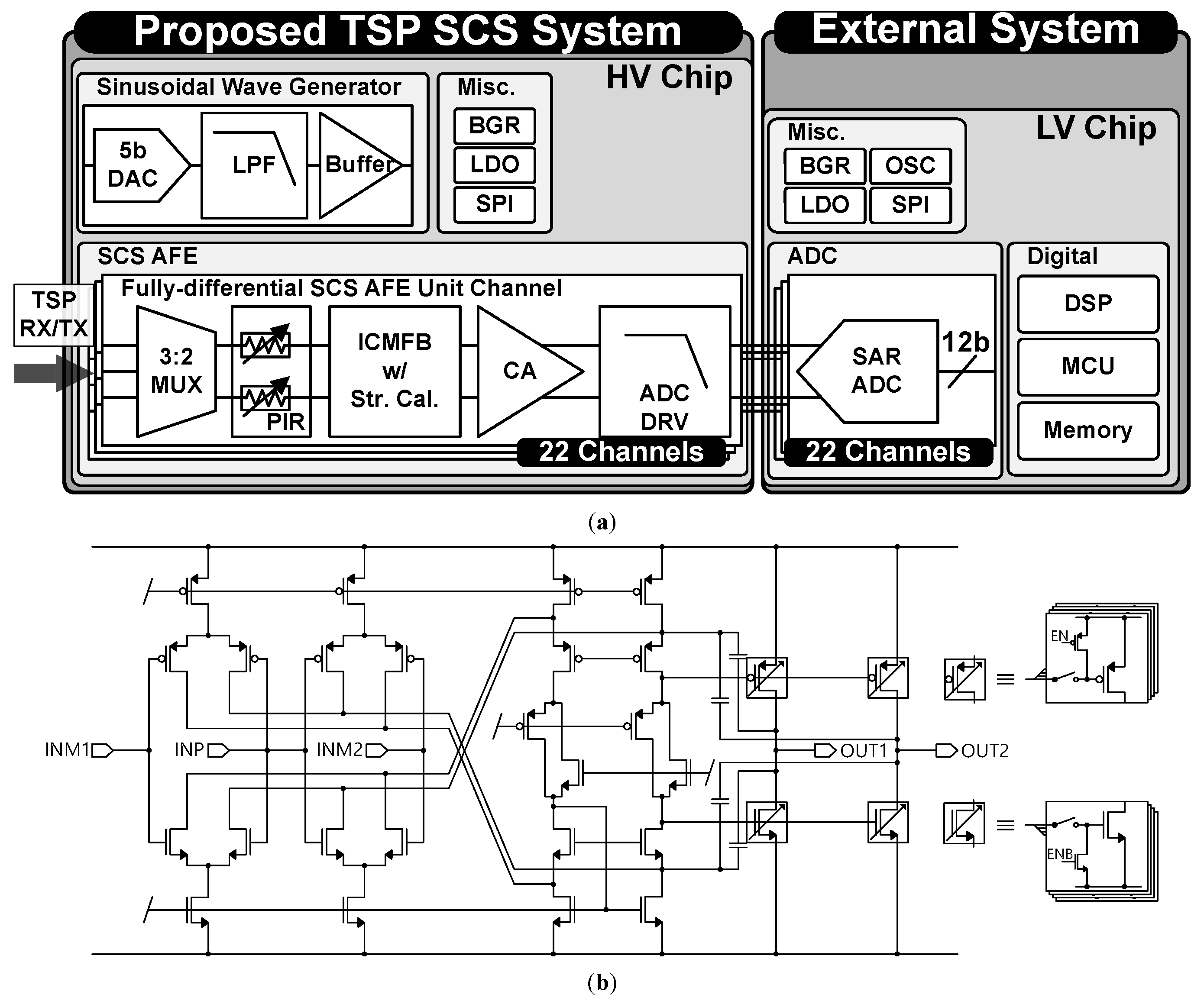
4. Implementation
Figure 6a illustrates the block diagram of the proposed TSP SCS system. The proposed work includes SCS AFE, sinusoidal wave generator, bandgap reference (BGR), low-dropout regulator (LDO), and serial peripheral interface (SPI) blocks in a high-voltage (HV) chip designed with a 130 nm CMOS process and 3
supply voltage. The proposed system is designed to work with an external low-voltage (LV) chip consisting of SAR ADC, digital blocks, and others. A 3:2 multiplexer (MUX) selects two adjacent TSP RX or TX electrodes to be sensed [
6,
9]. A sinusoidal wave generator generates a sinusoidal self-capacitance driving signal to minimize display image flickering due to the high voltage pulse wave driving [
10,
11]. The ICMFB drives the selected TSP electrodes pair with a 150
and 2.8 V
pp sinusoidal wave. A CA amplifies the input current difference due to the touch, and an ADC driver (ADC DRV) drives the input of SAR ADC in the external LV chip while providing anti-aliasing filtering. The LV chip samples AFE output, processes touch data using DSP, and controls both HV and LV chips with MCU.
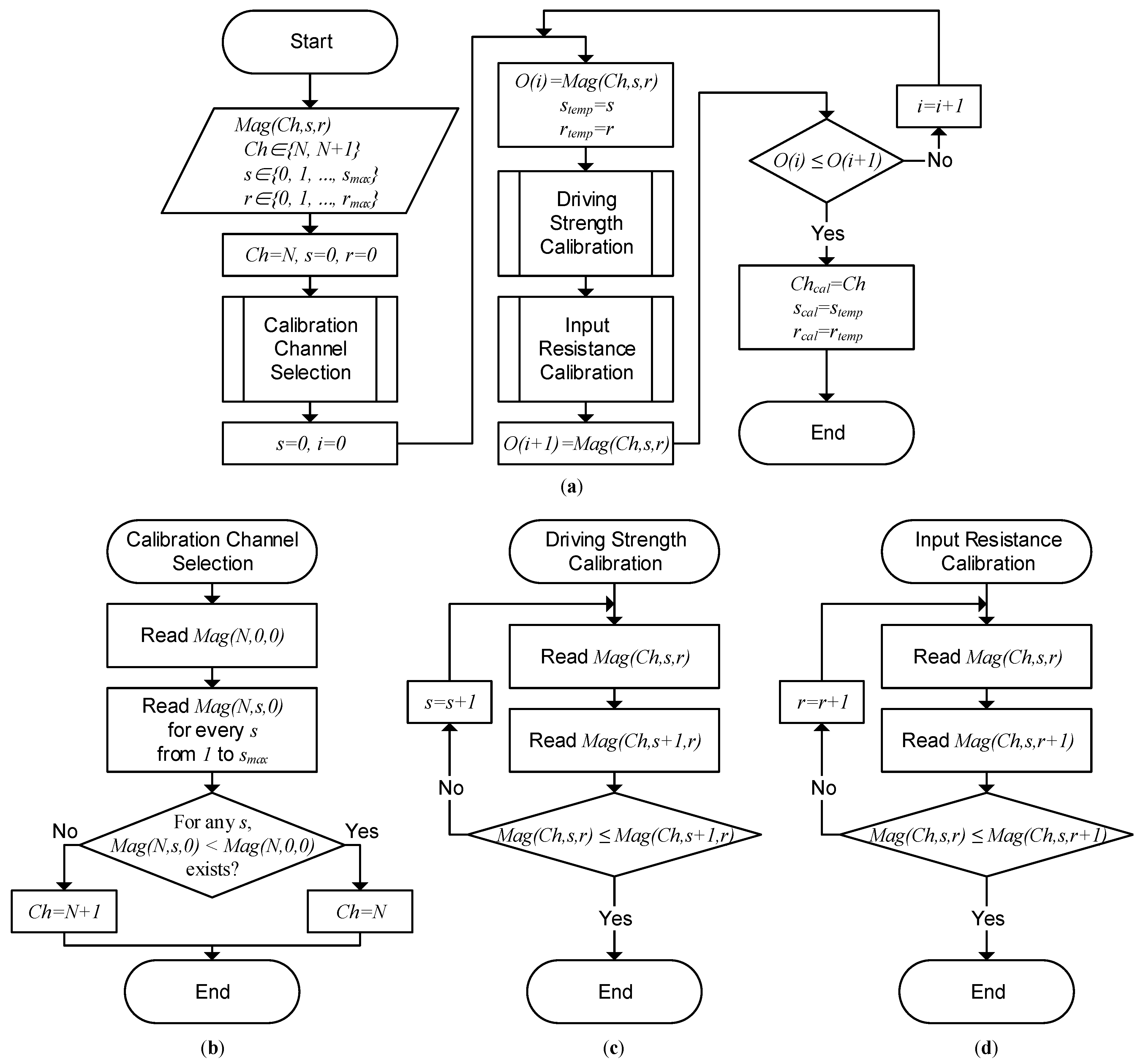
For the proposed self-capacitance mismatch calibration, a programmable input resistor (PIR) block and the ICMFB with a driving strength control feature are implemented. The PIR, which consists of a poly resistor and switch arrays, is implemented to introduce input series resistance difference between the fully-differential pairs. Due to the trade-off between the area consumption and the calibration resolution, the PIR is designed as a 3-bit control with 20
step.
Figure 6b shows the structure of ICMFB with driving strength control. The 4-bit binary driving strength control code selects the number of the output stage CMOS that should be turned on for OUT1 and OUT2 separately. Therefore, the ICMFB can introduce a driving strength difference up to 38.75%, with 1.25% LSB.
5. Simulation Results
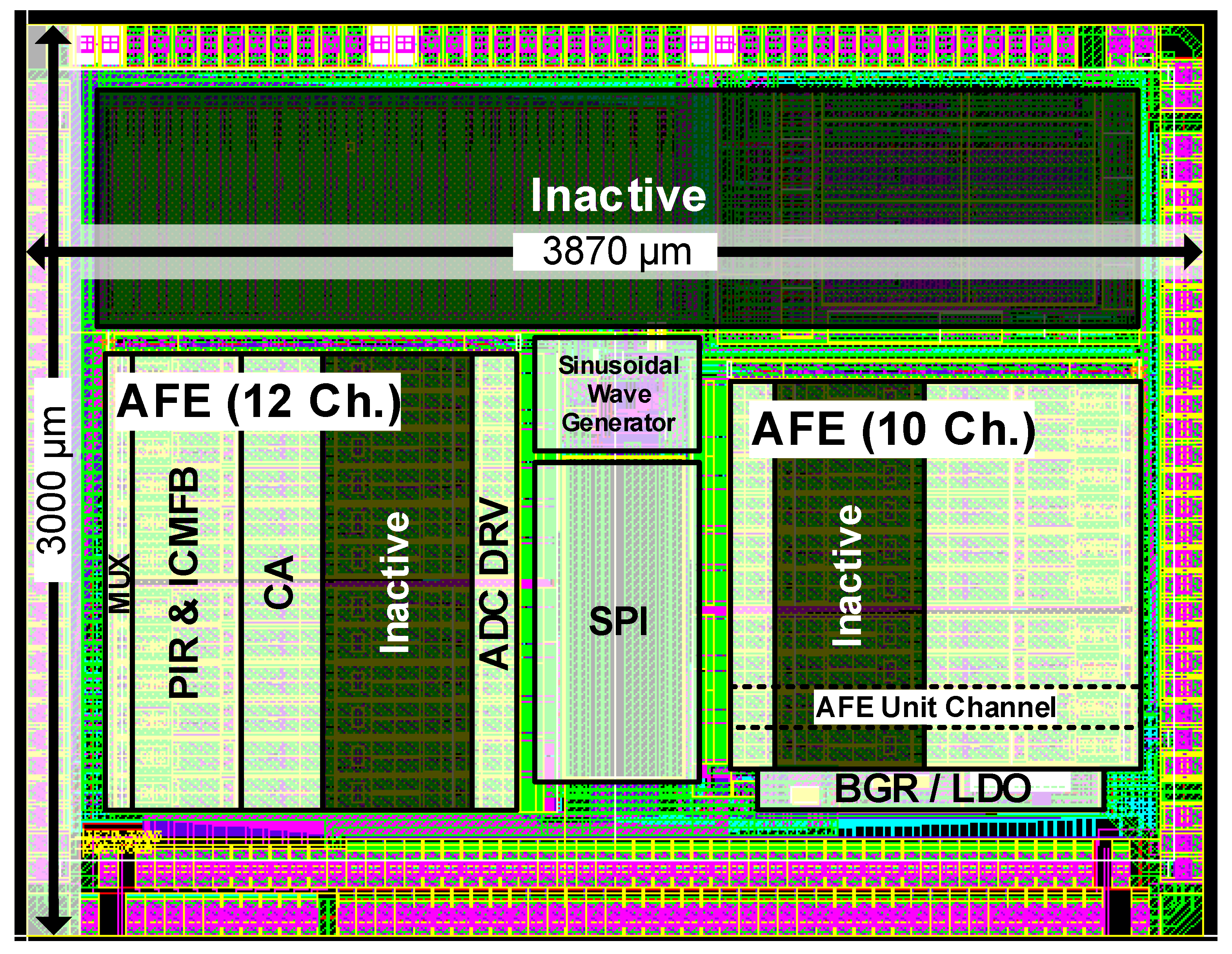
The proposed TSP SCS system is designed with a 130
CMOS process.
Figure 7 shows the layout of the proposed TSP SCS system. The active area of the proposed TSP SCS system is 3.15
.
Figure 8 shows the CA output before and after the proposed calibration. The driving signal is a 150
and 2.8 V
pp sinusoidal wave. An OLED TSP model with
and
was used for simulation. To assume the worst case, a 12% self-capacitance mismatch between RX electrodes was applied, which is equivalent to
mismatch. Therefore, the CA differential output was saturated before applying the proposed calibration. After the first cycle of the proposed calibration, the self-capacitance mismatch no longer caused saturation in the CA output. Thus, the self-capacitance variation by touch, which is 40
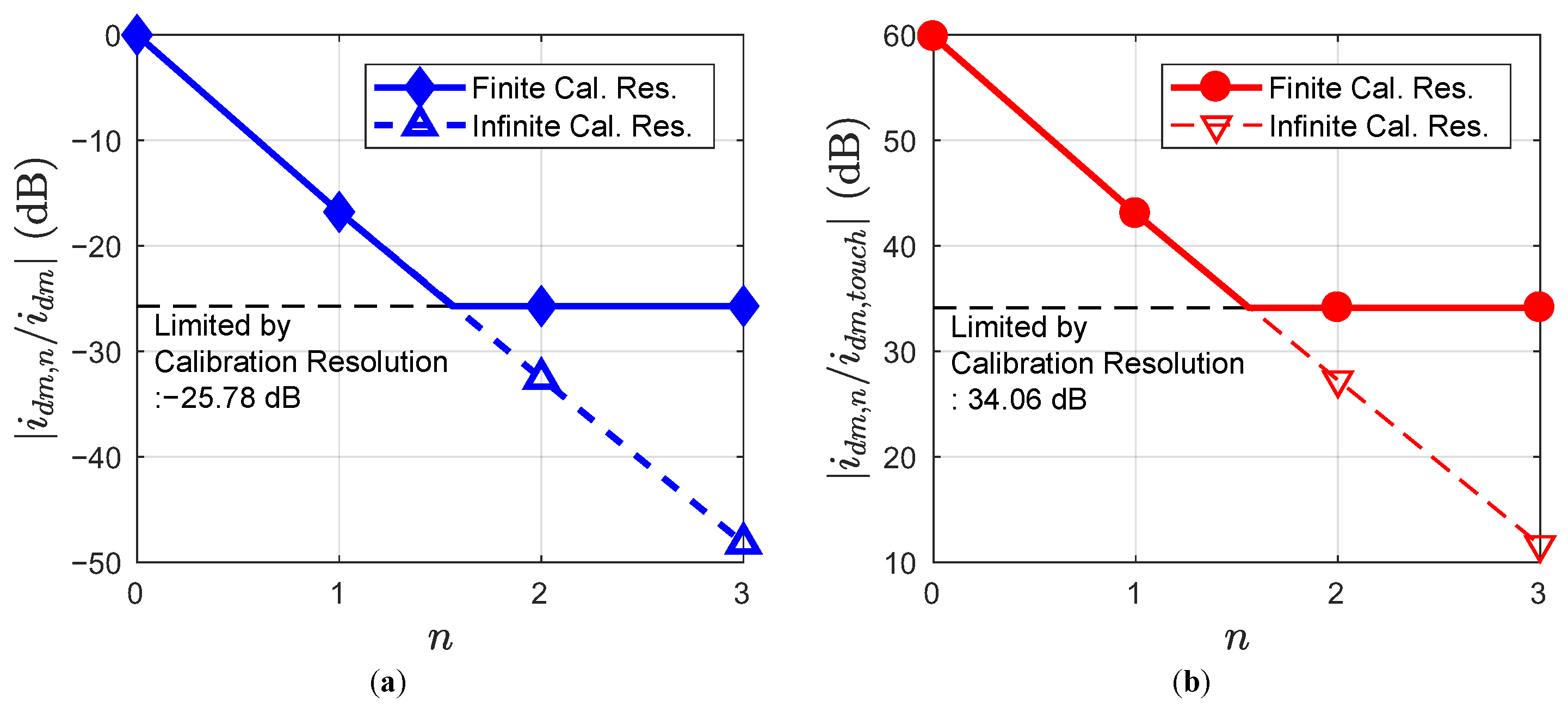
for our design target TSP model, is detectable by AFE. As the proposed calibration cycle is repeated, the output offset decreases. In other words, the headroom for the increased gain of AFE is acquired and the SNR of the SCS system is increased with the repetition of the proposed calibration cycles. Due to the limited calibration resolution and the large signal non-linearity of the ICMFB, the proposed calibration reached its maximum output offset removal performance after the two calibration cycles were performed.
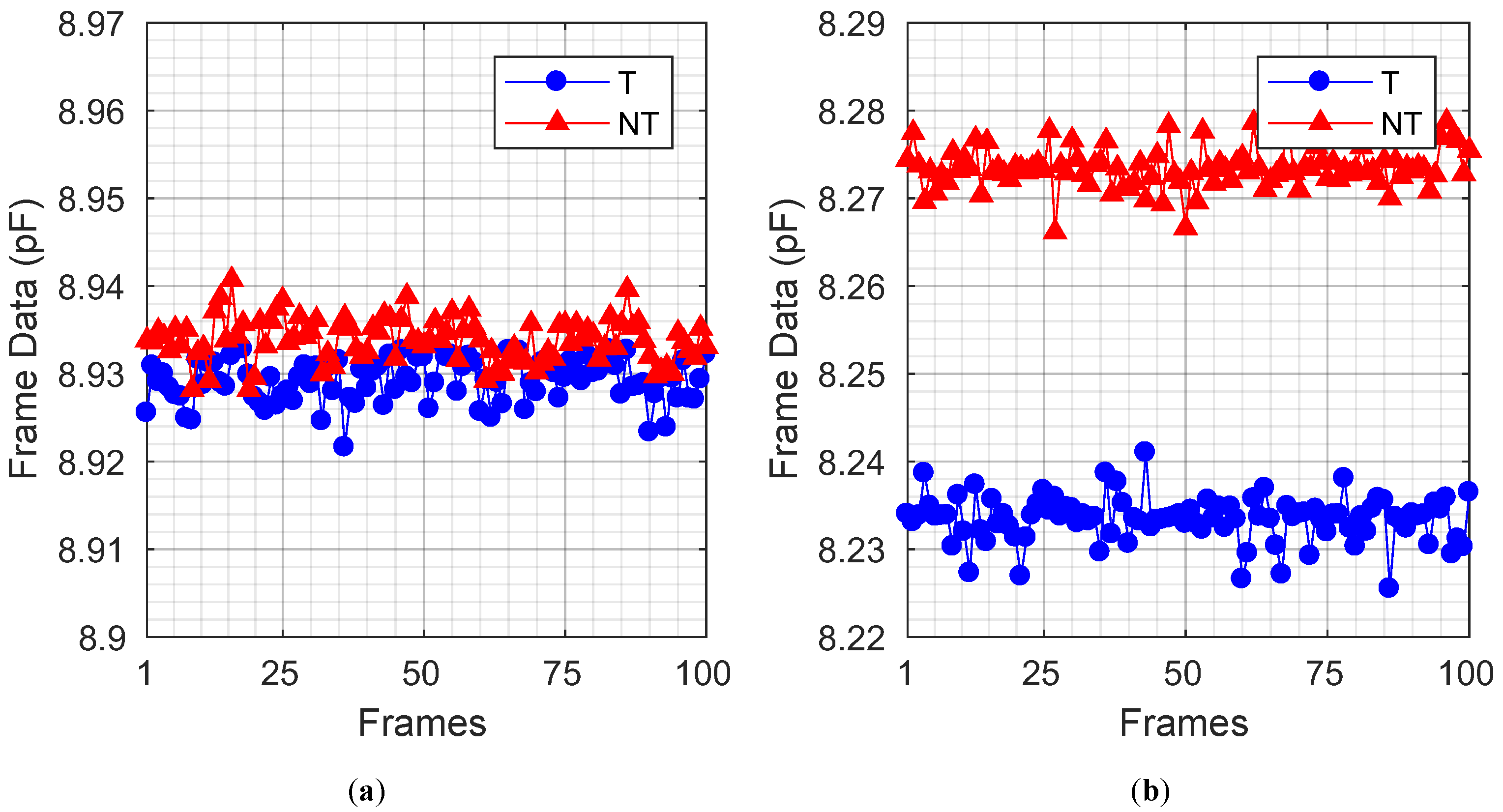
Figure 9 shows frame data plots before and after the proposed calibration. Each frame data was obtained by applying digital signal processing, which includes down-conversion, cascaded integrator-comb (CIC) filtering, and integration to each 2 ms time-domain data, resulting in a single integer value, called frame data. Therefore, the frame data represents the received touch signal intensity sensed over a 2 ms period. Note that, in
Figure 9, the unit of the frame data is converted to pF by correlating the difference between the average touch (T) and non-touch (NT) frame data to the known
value, which is provided by the TSP manufacturer. To obtain the SNR with a 120
frame rate, the duration of each time-domain data is 2
. The time-domain data include the circuit noise of the proposed TSP SCS system, as well as modeled external noise, such as display noise. The external noise was modeled using a method based on [
12]. Because of the saturation of the AFE, the TSP SCS system cannot distinguish touch (T) and non-touch (NT) state frame data, as shown in
Figure 9a. After the proposed calibration resolves the saturation, the T and NT frame data are now distributed separately without overlapping, making them distinguishable. Therefore, touch distinction becomes possible after the proposed calibration, as shown in
Figure 9b.
Table 1 compares the SNR of the proposed TSP SCS system before and after the proposed calibration is performed, in the presence of a 12% self-capacitance mismatch with a 120 Hz frame rate. SNR,
, and
were calculated from the frame data in
Figure 9, as follows: [
13,
14]
where
,
, and
are the
n-th frame data when touched, the average of 100 frame data when touched, and the average of 100 frame data when not touched, respectively.
is defined as the difference between
and
, and it represents the strength of touch signal variation caused by changes in
due to touch.
is the root-mean-square value of the 100 frame data when touched, with
as a baseline. Then, SNR is evaluated by dividing
by
. The proposed calibration resolves the saturation of the AFE stage and provides headroom for higher AFE gain, thereby increasing the SNR by
dB.
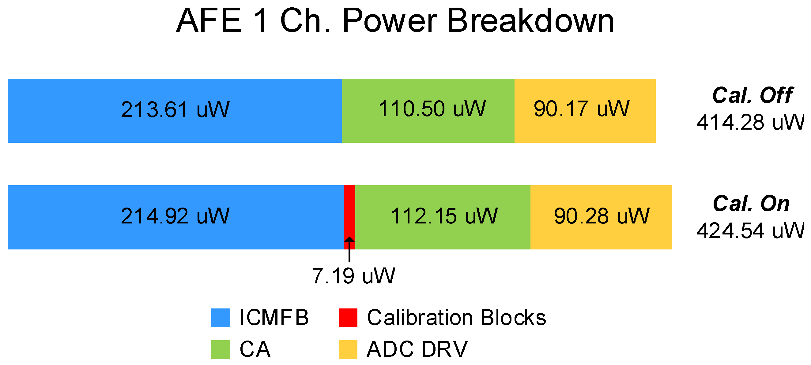
Figure 10 illustrates the power breakdown for a single AFE channel, comparing before and after the calibration is performed. In the “Cal.Off” state, the proposed calibration is turned off, and the self-capacitance mismatch is not modeled. As a result, the output offset is not generated in the “Cal. Off” state. In the “Cal.On” state, the proposed calibration has been performed, minimizing the output offset while exposed to 12% self-capacitance mismatch. The power breakdown shows that only an additional
is consumed after the proposed calibration is performed. Furthermore, the calibration blocks, including PIR and the switched output devices of ICMFB, consume
, which accounts for 1.69% of the total power consumption in the “Cal. On” state. Additionally, the calibration block only takes 6.31% of the active area in a single-channel AFE. These results demonstrate that the proposed calibration can be implemented with minimized power and area consumption, making it an efficient solution for addressing self-capacitance mismatches.
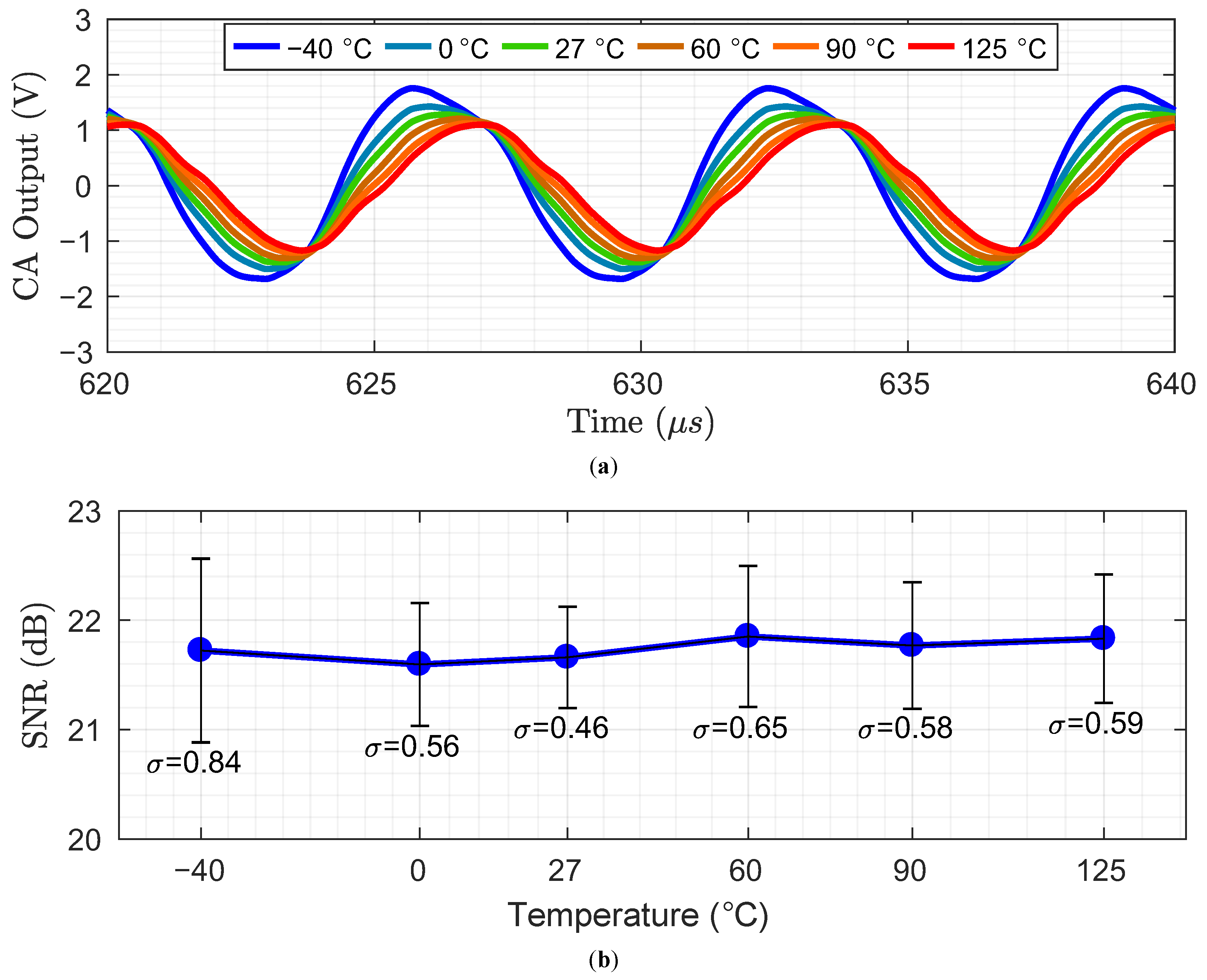
Figure 11 demonstrates the performance consistency of the system under temperature variation with optimal calibration setting found at 27
, while exposed to a 12% self-capacitance mismatch.
Figure 11a shows the CA output waveform variation. With the optimal calibration setting found at 27
, the CA output offset amplitude varies inversely with temperature changes. However, this temperature induced variation in the CA output offset does not cause saturation of the CA output, ensuring the proposed system’s SNR remains stable, as shown in
Figure 11b. For
Figure 11b, 10 SNR results are obtained at each temperature points, and their average is plotted. The error bars indicate the standard deviation of these results. This SNR result demonstrates that the system performance remains stable under temperature variation, even without updating the calibration setting for temperature change. Based on the demonstrated stable SNR performance under temperature variation without updating the calibration setting, the proposed calibration does not require adjustments for temperature variation.
Table 2 is the performance summary of the proposed TSP SCS system and the previous works. The proposed work achieves comparable 40.98 dB SNR with a 120 Hz frame rate while consuming 6.2 mW. Even under the worst self-capacitance mismatch case, the proposed SCS system was able to sense the self-capacitance variation by touch with 20.89 dB SNR after the proposed self-capacitance mismatch calibration was performed. Note that the fair comparison of SNR, power consumption, or FoM [
15] is difficult because they heavily depend on TSP electrical characteristics [
16].


