
Engineering of Advanced Materials for High Magnetic Field Sensing: A Review


Abstract
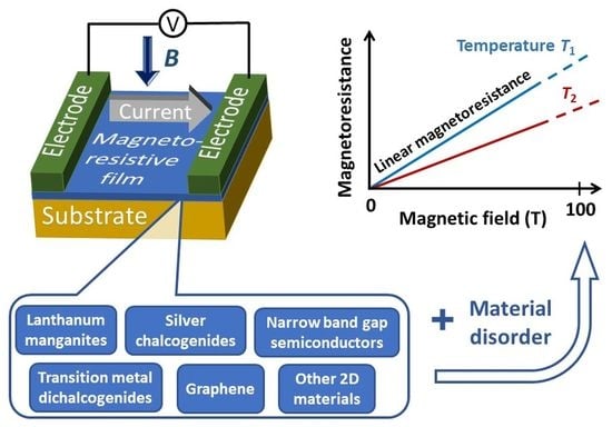
1. Introduction
2. Main Geometric Configurations of High-Field Magnetic Sensors Based on Solid-State Materials
2.1. Hall Sensors
2.2. Magnetoresistive Sensors
2.2.1. Conventional Magnetoresistance Configuration
2.2.2. Extraordinary Magnetoresistance Configuration
3. Colossal Magnetoresistance Materials
3.1. Lanthanum Manganites
3.1.1. Low-Field Magnetoresistance
3.1.2. High-Field Magnetoresistance

3.2. High-Field Magnetic Sensors Based on CMR Effect
4. Linear Magnetoresistance in Silver Chalcogenides and Narrow Bandgap Semiconductors
4.1. Magnetoresistance in Nonstoichiometric Silver Chalcogenides
4.2. Magnetoresistance in InSb
5. Single-Few-Layer Graphene
5.1. Magnetoresistance in Graphene
5.2. Magnetic Sensors Based on Graphene
6. Two-Dimensional Transition Metal Dichalcogenides
7. Summary and Outlook
Funding
Institutional Review Board Statement
Informed Consent Statement
Data Availability Statement
Acknowledgments
Conflicts of Interest
Abbreviations
| Acronym/abbreviation | Definition |
| 1LG | Single layer graphene |
| 2D | Two-dimensional |
| 3LG | Three-layer graphene |
| AMR | Anisotropic magnetoresistance |
| BP | Black phosphorus |
| CMR | Colossal magnetoresistance |
| EMR | Extraordinary magnetoresistance |
| FET | Field-effect transistor |
| GMI | Giant magnetoimpedance |
| GMR | Giant magnetoresistance |
| Gr | Graphene |
| h-BN | hexagonal boron nitride |
| HFMR | High-field magnetoresistance |
| LCMO | La1−xCaxMnO3 |
| LFMR | Low-field magnetoresistance |
| LMR | Linear magnetoresistance |
| LSMO | La1−xSrxMnyO3 |
| LSMCO | La1−xSrx(Mn1−yCoy)zO3 |
| MRA | Magnetoresistance anisotropy |
| MTJ | Magnetic tunnel junction |
| MR | Magnetoresistance |
| SdHO | Shubnikov-de Haas oscillations |
| SEM | Scanning electron microscopy |
| PL | Parish and Littlewood model |
| TEM | Transmission electron microscopy |
| TMDC | Transition metal dichalcogenide |
| TMR | Tunneling magnetoresistance |
| TRL | Technology readiness levels |
| VRH | Variable range hopping |
References
- Jogschies, L.; Klaas, D.; Kruppe, R.; Rittinger, J.; Taptimthong, P.; Wienecke, A.; Rissing, L.; Wurz, M.C. Recent developments of magnetoresistive sensors for industrial applications. Sensors 2015, 15, 28665. [Google Scholar] [CrossRef] [PubMed]
- Lenz, J.; Edelstein, S. Magnetic Sensors and Their Applications. IEEE Sens. J. 2006, 6, 631–649. [Google Scholar] [CrossRef]
- Yole Développement. Magnetic Sensor Market and Technologies Report from Yole Développement. 2017. Available online: http://www.yole.fr/Magnetic_Sensor_Market.aspx#.WmoQO3mLlaQ (accessed on 5 May 2022).
- Zheng, C.; Zhu, K.; Cardoso de Freitas, S.; Chang, J.-Y.; Davies, J.E.; Eames, P.; Freitas, P.P.; Kazakova, O.; Kim, C.G.; Leung, C.-W.; et al. Magnetoresistive sensor development roadmap (non-recording applications). IEEE Trans. Magn. 2019, 55, 0800130. [Google Scholar] [CrossRef]
- Khan, M.A.; Sun, J.; Li, B.; Przybysz, A.; Kosel, J. Magnetic sensors-A review and recent technologies. Eng. Res. Express 2021, 3, 022005. [Google Scholar] [CrossRef]
- Costa, T.; Cardoso, F.A.; Germano, J.; Freitas, P.P.; Piedade, M.S. A CMOS Front-End with Integrated Magnetoresistive Sensors for Biomolecular Recognition Detection Applications. IEEE Trans. Biomed. Circuits Syst. 2017, 11, 988–1000. [Google Scholar] [CrossRef] [PubMed]
- Pla, D.; Jimenez, C.; Burriel, M. Engineering of Functional Manganites Grown by MOCVD for Miniaturized Devices. Adv. Mater. Interfaces 2017, 4, 1600974. [Google Scholar] [CrossRef]
- Israel, C.; Calderón, M.J.; Mathur, N.D. The Current Spin on Manganites. Mater. Today 2007, 10, 24–32. [Google Scholar] [CrossRef]
- Sensitec Katalog. Magnetic Micro- and Nanotechnology for Robust Sensor Solutions. Available online: https://www.sensitec.com/fileadmin/sensitec/Service_and_Support/Downloads/Catalogue/Sensitec_Katalog2015_Web_LZen.pdf (accessed on 26 January 2018).
- Stankevič, T.; Medišauskas, L.; Stankevič, V.; Balevičius, S.; Žurauskienė, N.; Liebfried, O.; Schneider, M. Pulsed Magnetic Field Measurement System Based on Colossal Magnetoresistance-B-Scalar Sensors for Railgun Investigation. Rev. Sci. Instrum. 2014, 85, 044704. [Google Scholar] [CrossRef]
- Stankevič, V.; Keršulis, S.; Dilys, J.; Bleizgys, V.; Viliūnas, M.; Vertelis, V.; Maneikis, A.; Rudokas, V.; Plaušinaitienė, V.; Žurauskienė, N. Measurement System for Short-Pulsed Magnetic Fields. Sensors 2023, 23, 1435. [Google Scholar] [CrossRef]
- Lukose, R.; Zurauskiene, N.; Stankevic, V.; Vagner, M.; Plausinaitiene, V.; Niaura, G.; Kersulis, S.; Balevicius, S.; Bolli, E.; Mezzi, A.; et al. Room Temperature Co-Doped Manganite/Graphene Sensor Operating at High Pulsed Magnetic Fields. Sci. Rep. 2019, 9, 1–10. [Google Scholar] [CrossRef]
- Battesti, R.; Beard, J.; Böser, S.; Bruyant, N.; Budker, D.; Crooker, S.A.; Daw, E.J.; Flambaum, V.V.; Inada, T.; Irastorza, I.G.; et al. High Magnetic Fields for Fundamental Physics. Phys. Rep. 2018, 765–766, 1–39. [Google Scholar] [CrossRef]
- Matsui, K.; Kanda, T.; Ihara, Y.; Kindo, K.; Kohama, Y. Compact Megajoule-Class Pulsed Power Supply for Generating Long-Pulsed Magnetic Fields. Rev. Sci. Instrum. 2021, 92, 024711. [Google Scholar] [CrossRef] [PubMed]
- Kohama, Y.; Nomura, T.; Zherlitsyn, S.; Ihara, Y. Time-Resolved Measurements in Pulsed Magnetic Fields. J. Appl. Phys. 2022, 132, 070903. [Google Scholar] [CrossRef]
- Tumanski, S. Indution coil sensors—A review. Technology 2007, 18, R31–R46. [Google Scholar] [CrossRef]
- Nomura, T.; Hauspurg, A.; Gorbunov, D.I.; Miyata, A.; Schulze, E.; Zvyagin, S.A.; Tsurkan, V.; Matsuda, Y.H.; Kohama, Y.; Zherlitsyn, S. Ultrasound Measurement Technique for the Single-Turn-Coil Magnets. Rev. Sci. Instrum. 2021, 92, 063902. [Google Scholar] [CrossRef] [PubMed]
- Haran, T.L.; Hoffman, R.B.; Lane, S.E. Diagnostic capabilities for electromagnetic railguns. IEEE Trans. Plasma Sci. 2013, 41, 1526–1532. [Google Scholar] [CrossRef]
- Mihailovic, P.; Petricevic, S. Fiber Optic Sensors Based on the Faraday Effect. Sensors 2021, 21, 6564. [Google Scholar] [CrossRef] [PubMed]
- Bolshakova, I.; Bulavin, M.; Kargin, N.; Kost, Y.; Kuech, T.; Kulikov, S.; Radishevskiy, M.; Shurygin, F.; Strikhanov, M.; Vasil’evskii, I.; et al. Metal Hall Sensors for the New Generation Fusion Reactors of DEMO Scale. Nucl. Fusion 2017, 57, 116042. [Google Scholar] [CrossRef]
- Mironov, O.A.; Zherlitsyn, S.; Uhlarz, M.; Skourski, Y.; Palewski, T.; Wosnitza, J. Microminiature Hall Probes for Applications at Pulsed Magnetic Fields up to 87 Tesla. J. Low Temp. Phys. 2010, 159, 315–318. [Google Scholar] [CrossRef]
- Karsenty, A. A Comprehensive Review of Integrated Hall Effects in Macro-, Micro-, Nanoscales, and Quantum Devices. Sensors 2020, 20, 4163. [Google Scholar] [CrossRef]
- Collomb, D.; Li, P.; Bending, S. Frontiers of Graphene-Based Hall-Effect Sensors. J. Phys. Condens. Matter 2021, 33, 243002. [Google Scholar] [CrossRef] [PubMed]
- Schroder, D.K. Semiconductor Material and Device Characterization; John Wiley & Sons, Inc.: Hoboken, NJ, USA, 2005. [Google Scholar] [CrossRef]
- Look, D.C. Review of Hall Effect and Magnetoresistance Measurements in GaAs Materials and Devices. J. Electrochem. Soc. 1990, 137, 260–266. [Google Scholar] [CrossRef]
- Lippmann, H.-J.; Kuhrt, F. Der Geometrieeinfluß Auf Den Hall-Effekt Bei Rechteckigen Halbleiterplatten. Z. Für Nat. A 1958, 13, 474–483. [Google Scholar] [CrossRef]
- Harrysson Rodrigues, I.; Generalov, A.; Md Hoque, A.; Soikkeli, M.; Murros, A.; Arpiainen, S.; Vorobiev, A. Geometrical Magnetoresistance Effect and Mobility in Graphene Field-Effect Transistors. Appl. Phys. Lett. 2022, 121, 013502. [Google Scholar] [CrossRef]
- Balevičius, S.; Stankevič, V.; Žurauskienė, N.; Šimkevičius, Č.; Liebfried, O.; Löffler, M.; Schneider, M.; Abrutis, A.; Plaušinaitienė, V. Thin Film Manganite-Metal Interconnection and “Loop Effect” Studies in CMR-Based High Magnetic Field Sensors. Acta Phys. Pol. A 2009, 115, 1133–1135. [Google Scholar] [CrossRef]
- Solin, S.A.; Thio, T.; Hines, D.R.; Heremans, J.J. Enhanced Room-Temperature Geometric Magnetoresistance in Inhomogeneous Narrow-Gap Semiconductors. Science 2000, 289, 1530–1532. [Google Scholar] [CrossRef]
- Sun, J.; Kosel, J. Extraordinary Magnetoresistance in Semiconductor/Metal Hybrids: A Review. Materials 2013, 6, 500–516. [Google Scholar] [CrossRef]
- Pisana, S.; Braganca, P.M.; Marinero, E.E.; Gurney, B.A. Tunable Nanoscale Graphene Magnetometers. Nano Lett. 2009, 10, 341–346. [Google Scholar] [CrossRef]
- Holz, M.; Kronenwerth, O.; Grundler, D. Enhanced Sensitivity due to Current Redistribution in the Hall Effect of Semiconductor-Metal Hybrid Structures. Appl. Phys. Lett. 2005, 86, 072513. [Google Scholar] [CrossRef]
- Sun, J.; Patil, S.B.; Soh, Y.-A.; Kosel, J. Strong Temperature Dependence of Extraordinary Magnetoresistance Correlated to Mobility in a Two-Contact Device. Appl. Phys. Express 2012, 5, 033002. [Google Scholar] [CrossRef]
- Jonker, G.H.; Van Santen, J.H. Ferromagnetic Compounds of Manganese with Perovskite Structure. Physica 1950, 16, 337–349. [Google Scholar] [CrossRef]
- Van Santen, J.H.; Jonker, G.H. Electrical Conductivity of Ferromagnetic Compounds of Manganese with Perovskite Structure. Physica 1950, 16, 599–600. [Google Scholar] [CrossRef]
- Jonker, G.H. Magnetic Compounds with Perovskite Structure IV Conducting and Non-Conducting Compounds. Physica 1956, 22, 707–722. [Google Scholar] [CrossRef]
- Volger, J. Further Experimental Investigations on Some Ferromagnetic Oxidic Compounds of Manganese with Perovskite Structure. Physica 1954, 20, 49–66. [Google Scholar] [CrossRef]
- von Helmolt, R.; Wecker, J.; Holzapfel, B.; Schultz, L.; Samwer, K. Giant Negative Magnetoresistance in Perovskitelike La2/3Ba1/3MnOX Ferromagnetic Films. Phys. Rev. Lett. 1993, 71, 2331–2333. [Google Scholar] [CrossRef]
- Jin, S.; Tiefel, T.H.; McCormack, M.; Fastnacht, R.A.; Ramesh, R.; Chen, L.H. Thousandfold Change in Resistivity in Magnetoresistive La-Ca-Mn-O Films. Science 1994, 264, 413–415. [Google Scholar] [CrossRef]
- Levy, P.M. Giant Magnetoresistance in Magnetic Layered and Granular Materials. Science 1992, 256, 972–973. [Google Scholar] [CrossRef]
- Urushibara, A.; Moritomo, Y.; Arima, T.; Asamitsu, A.; Kido, G.; Tokura, Y. Insulator-Metal Transition and Giant Magnetoresistance inLa1−XSrXMnO3. Phys. Rev. B 1995, 51, 14103–14109. [Google Scholar] [CrossRef]
- Tomioka, Y.; Asamitsu, A.; Tokura, Y. Magnetotransport Properties and Magnetostructural Phenomenon in Single Crystals of La0.7(Ca1−YSrY)0.3MnO3. Phys. Rev. B 2000, 63, 024421. [Google Scholar] [CrossRef]
- Bebenin, N.G.; Ustinov, V.V. Conduction and Disorder in -Based Materials. J. Phys. Condens. Matter 1998, 10, 6301–6309. [Google Scholar] [CrossRef]
- Millis, A.J.; Littlewood, P.B.; Shraiman, B.I. Double Exchange Alone Does Not Explain the Resistivity Of La1−XSrxMnO3. Phys. Rev. Lett. 1995, 74, 5144–5147. [Google Scholar] [CrossRef] [PubMed]
- Coey, J.M.D.; Viret, M.; von Molnár, S. Mixed-Valence Manganites. Adv. Phys. 2009, 58, 571–697. [Google Scholar] [CrossRef]
- Dagotto, E.; Hotta, T.; Moreo, A. Colossal Magnetoresistant Materials: The Key Role of Phase Separation. Phys. Rep. 2001, 344, 1–153. [Google Scholar] [CrossRef]
- Salamon, M.B.; Jaime, M. The Physics of Manganites: Structure and Transport. Rev. Mod. Phys. 2001, 73, 583–628. [Google Scholar] [CrossRef]
- Ziese, M. Extrinsic Magnetotransport Phenomena in Ferromagnetic Oxides. Rep. Prog. Phys. 2002, 65, 143–249. [Google Scholar] [CrossRef]
- Haghiri-Gosnet, A.-M.; Renard, J.-P. CMR Manganites: Physics, Thin Films and Devices. J. Phys. D Appl. Phys. 2003, 36, R127–R150. [Google Scholar] [CrossRef]
- Tendeloo, G.V.; Lebedev, O.I.; Hervieu, M.; Raveau, B. Structure and Microstructure of Colossal Magnetoresistant Materials. Rep. Prog. Phys. 2004, 67, 1315–1365. [Google Scholar] [CrossRef]
- Goodenough, J.B. Electronic and Ionic Transport Properties and Other Physical Aspects of Perovskites. Rep. Prog. Phys. 2004, 67, 1915–1993. [Google Scholar] [CrossRef]
- Tokura, Y. Critical Features of Colossal Magnetoresistive Manganites. Rep. Prog. Phys. 2006, 69, 797–851. [Google Scholar] [CrossRef]
- Israel, C.; Calderon, M.J.; Mathur, N.D. ChemInform Abstract: The Current Spin on Manganites. ChemInform 2008, 39. [Google Scholar] [CrossRef]
- Pękała, M.; Pękała, K.; Drozd, V. Magnetotransport Study of Nanocrystalline and Polycrystalline Manganites La0.8Sr0.2MnO3 in High Magnetic Fields. J. Appl. Phys. 2015, 117, 175902. [Google Scholar] [CrossRef]
- Pradhan, A.K.; Roul, B.K.; Wen, J.G.; Ren, Z.F.; Muralidhar, M.; Dutta, P.; Sahu, D.R.; Mohanty, S.; Patro, P.K. Enhanced Room-Temperature Magnetoresistance in Partially Melted La0.67Ca0.33MnO3 Manganites. Appl. Phys. Lett. 2000, 76, 763–765. [Google Scholar] [CrossRef]
- Zurauskiene, N.; Balevicius, S.; Stankevic, V.; Kersulis, S.; Klimantavicius, J.; Plausinaitiene, V.; Kubilius, V.; Skapas, M.; Juskenas, R.; Navickas, R. Magnetoresistive Properties of Thin Nanostructured Manganite Films Grown by Metalorganic Chemical Vapour Deposition onto Glass-Ceramics Substrates. J. Mater. Sci. 2018, 53, 12996–13009. [Google Scholar] [CrossRef]
- Hwang, H.Y.; Cheong, S.-W.; Ong, N.P.; Batlogg, B. Spin-Polarized Intergrain Tunneling inLa2/3Sr1/3MnO3. Phys. Rev. Lett. 1996, 77, 2041–2044. [Google Scholar] [CrossRef] [PubMed]
- Lee, S.; Hwang, H.Y.; Shraiman, B.I.; Ratcliff, W.D., II; Cheong, S.-W. Intergrain magnetoresistance via second-order tunneling in perovskite manganites. Phys. Rev. Lett. 1999, 82, 4508–4511. [Google Scholar] [CrossRef]
- Evetts, J.E.; Blamire, M.G.; Mathur, N.D.; Isaac, S.P.; Teo, B.-S.; Cohen, L.F.; Macmanus-Driscoll, J.L. Defect-Induced Spin Disorder and Magnetoresistance in Single-Crystal and Polycrystal Rare-Earth Manganite Thin Films. Philos. Trans. R. Soc. Lond. Ser. A Math. Phys. Eng. Sci. 1998, 356, 1593–1615. [Google Scholar] [CrossRef]
- Wagner, P.H.; Metlushko, V.; Trappeniers, L.; Vantomme, A.; Vanacken, J.; Kido, G.; Moshchalkov, V.V.; Bruynseraede, Y. Magnetotransport in Epitaxial Thin Films of the Magnetic PerovskitePr0.5Sr0.5MnO3. Phys. Rev. B 1997, 55, 3699–3707. [Google Scholar] [CrossRef]
- Wagner, P.; Gordon, I.; Trappeniers, L.; Vanacken, J.; Herlach, F.; Moshchalkov, V.V.; Bruynseraede, Y. Spin Dependent Hopping and Colossal Negative Magnetoresistance in EpitaxialNd0.52Sr0.48MnO3Films in Fields up to 50 T. Phys. Rev. Lett. 1998, 81, 3980–3983. [Google Scholar] [CrossRef]
- Balevičius, S.; Žurauskienė, N.; Stankevič, V.; Keršulis, S.; Plaušinaitienė, V.; Abrutis, A.; Zherlitsyn, S.; Herrmannsdörfer, T.; Wosnitza, J.; Wolff-Fabris, F. Nanostructured Thin Manganite Films in Megagauss Magnetic Field. Appl. Phys. Lett. 2012, 101, 092407. [Google Scholar] [CrossRef]
- Lu, Y.; Li, X.W.; Gong, G.Q.; Xiao, G.; Gupta, A.; Lecoeur, P.; Sun, J.Z.; Wang, Y.Y.; Dravid, V.P. Large magnetotunneling effect at low magnetic fields in micrometer-scale epitaxial La0.67Sr0.33MnO3 tunnel junctions. Phys. Rev. B. 1996, 54, R8357–R8360. [Google Scholar] [CrossRef]
- Ning, X.; Wang, Z.; Zhang, Z. Large, temperature-tunable low-field magnetoresistance in La0.7Sr0.3MnO3:NiO nanocomposite films modulated by microstructures. Adv. Funct. Mater. 2014, 24, 5393–5401. [Google Scholar] [CrossRef]
- Siwach, P.K.; Srivastava, P.; Singh, J.; Singha, H.K.; Srivastava, O.N. Broad temperature range low field magnetoresistance in La0.7Ca0.3MnO3:nano-ZnO composites. J. Alloys Compd. 2009, 481, 17–21. [Google Scholar] [CrossRef]
- Gao, X.; Li, L.; Jian, J.; Huang, J.; Sun, X.; Zhang, D.; Wang, H. Tunable low-field magnetoresistance properties in (La0.7Ca0.3MnO3)1−x:(CeO2)x vertically aligned nanocomposite thin films. Appl. Phys. Lett. 2019, 115, 053103. [Google Scholar] [CrossRef]
- Sadhu, A.; Bhattacharyya, S. Enhanced Low-Field Magnetoresistance in La0.71Sr0.29MnO3 Nanoparticles Synthesized by the Nonaqueous Sol–Gel Route. Chem. Mater. 2014, 26, 1702–1710. [Google Scholar] [CrossRef]
- Stankevic, V.; Zurauskiene, N.; Kersulis, S.; Plausinaitiene, V.; Lukose, R.; Klimantavicius, J.; Tolvaišienė, S.; Skapas, M.; Selskis, A.; Balevicius, S. Nanostructured Manganite Films Grown by Pulsed Injection MOCVD: Tuning Low- and High-Field Magnetoresistive Properties for Sensors Applications. Sensors 2022, 22, 605. [Google Scholar] [CrossRef]
- Zurauskiene, N.; Stankevic, V.; Kersulis, S.; Vagner, M.; Plausinaitiene, V.; Dobilas, J.; Vasiliauskas, R.; Skapas, M.; Koliada, M.; Pietosa, J.; et al. Enhancement of Room-Temperature Low-Field Magnetoresistance in Nanostructured Lanthanum Manganite Films for Magnetic Sensor Applications. Sensors 2022, 22, 4004. [Google Scholar] [CrossRef]
- Balcells, L.; Fontcuberta, J.; Martínez, B.; Obradors, X. High-Field Magnetoresistance at Interfaces in Manganese Perovskites. Phys. Rev. B 1998, 58, R14697–R14700. [Google Scholar] [CrossRef]
- Kozlova, N.; Dörr, K.; Eckert, D.; Walter, T.; Müller, K.-H. Intergrain Magnetoresistance of La0.7Sr0.3MnO3 in Pulsed Magnetic Fields up to 50T. J. Magn. Magn. Mater. 2003, 261, 48–55. [Google Scholar] [CrossRef]
- Pękała, M.; Kozlova, N.; Drozd, V. Comparison of Magnetotransport Properties of Nano- and Microcrystalline La0.7Ca0.3MnO3 Manganites in High Magnetic Field. J. Appl. Phys. 2008, 104, 123902. [Google Scholar] [CrossRef]
- Tokunaga, M.; Miura, N.; Tomioka, Y.; Tokura, Y. High-Field Magnetization Process in R1/2Ca1/2MnO3(R=Sm and Y) up to 100 T. Phys. Rev. B 1999, 60, 6219–6222. [Google Scholar] [CrossRef]
- Gangineni, R.B.; Dörr, K.; Kozlova, N.; Nenkov, K.; Müller, K.-H.; Schultz, L.; Seetha Lakshmi, L. Dependence of the High-Field Grain-Boundary Magnetoresistance of Ferromagnetic Manganites on Curie Temperature. J. Appl. Phys. 2006, 99, 053904. [Google Scholar] [CrossRef]
- Zurauskiene, N.; Balevicius, S.; Pavilonis, D.; Stankevic, V.; Plausinaitiene, V.; Zherlitsyn, S.; Herrmannsdorfer, T.; Law, J.M.; Wosnitza, J. Magnetoresistance and Resistance Relaxation of Nanostructured La-Ca-MnO Films in Pulsed Magnetic Fields. IEEE Trans. Magn. 2014, 50, 1–4. [Google Scholar] [CrossRef]
- Zurauskiene, N.; Skapas, M.; Juskenas, R.; Knasiene, B.; Naujalis, E.; Law, J.M.; Pavilonis, D.; Klimantavicius, J.; Balevicius, S.; Stankevic, V.; et al. Influence of MOCVD Growth Pressure on Magnetoresistance of Nanostructured La-Ca-Mn-O Films Used for Magnetic Field Sensors. IEEE Trans. Plasma Sci. 2017, 45, 2780–2786. [Google Scholar] [CrossRef]
- Žurauskienė, N.; Rudokas, V.; Keršulis, S.; Stankevič, V.; Pavilonis, D.; Plaušinaitienė, V.; Vagner, M.; Balevičius, S. Magnetoresistance and Its Relaxation of Nanostructured La-Sr-Mn-Co-O Films: Application for Low Temperature Magnetic Sensors. J. Magn. Magn. Mater. 2021, 539, 168340. [Google Scholar] [CrossRef]
- Rudokas, V.; Skapas, M.; Arsenijevic, S.; Zurauskiene, N.; Lukose, R.; Kersulis, S.; Stankevic, V.; Pavilonis, D.; Balevicius, S.; Plausinaitiene, V.; et al. La–Sr–Mn–Co–O Films for High Pulsed Magnetic Field Measurements at Cryogenic Temperatures. IEEE Trans. Plasma Sci. 2019, 47, 4541–4546. [Google Scholar] [CrossRef]
- Novosel, N.; Rivas Góngora, D.; Jagličić, Z.; Tafra, E.; Basletić, M.; Hamzić, A.; Klaser, T.; Skoko, Ž.; Salamon, K.; Kavre Piltaver, I.; et al. Grain-Size-Induced Collapse of Variable Range Hopping and Promotion of Ferromagnetism in Manganite La0.5Ca0.5MnO3. Crystals 2022, 12, 724. [Google Scholar] [CrossRef]
- Xu, Y.; Memmert, U.; Hartmann, U. Magnetic Field Sensors from Polycrystalline Manganites. Sens. Actuators A Phys. 2001, 91, 26–29. [Google Scholar] [CrossRef]
- Krichene, A.; Boujelben, W.; Mukherjee, S.; Shah, N.A.; Solanki, P.S. An Empirical Model for Magnetic Field Dependent Resistivity and Magnetoresistance in Manganites: Application on Polycrystalline Charge-Ordered La0.4Gd0.1ca0.5MnO3. Phys. Chem. Chem. Phys. 2018, 20, 12608–12617. [Google Scholar] [CrossRef]
- Dhieb, S.; Krichene, A.; Fettar, F.; Chniba Boudjada, N.; Boujelben, W. Stability of Charge Ordering in La0.5−XHoXCa0.5MnO3 Polycrystalline Manganites. Appl. Phys. A 2021, 127, 700. [Google Scholar] [CrossRef]
- Das, K.; Dasgupta, P.; Poddar, A.; Das, I. Significant Enhancement of Magnetoresistance with the Reduction of Particle Size in Nanometer Scale. Sci. Rep. 2016, 6, 20351. [Google Scholar] [CrossRef]
- Gamzatov, A.G.; Gadzhimuradov, T.A. Low-Temperature Intergranular Spin Transport in La0.5Ca0.4Li0.1MnO3 Manganite Under High Magnetic Field (1T≤H≤14T). J. Low Temp. Phys. 2016, 185, 590–596. [Google Scholar] [CrossRef]
- Yang, S.; Zhang, J. Current Progress of Magnetoresistance Sensors. Chemosensors 2021, 9, 211. [Google Scholar] [CrossRef]
- Xu, Y.; Dworak, V.; Drechsler, A.; Hartmann, U. Anisotropic Low-Field Magnetoresistance of Polycrystalline Manganite Sensors. Appl. Phys. Lett. 1999, 74, 2513–2515. [Google Scholar] [CrossRef]
- Rajapitamahuni, A.; Zhang, L.; Koten, M.A.; Singh, V.R.; Burton, J.D.; Tsymbal, E.Y.; Shield, J.E.; Hong, X. Giant Enhancement of Magnetic Anisotropy in Ultrathin Manganite Films via Nanoscale 1D Periodic Depth Modulation. Phys. Rev. Lett. 2016, 116, 187201. [Google Scholar] [CrossRef] [PubMed]
- Žurauskienė, N.; Keršulis, S.; Medišauskas, L.; Tolvaišienė, S. Investigation of Magnetoresistance and Its Anisotropy of Thin Polycrystalline La0.83Sr0.17MnO3Films in High Pulsed Magnetic Fields. Acta Phys. Pol. A 2011, 119, 186–188. [Google Scholar] [CrossRef]
- Schneider, M.; Schneider, R.; Stankevic, V.; Balevicius, S.; Zurauskien, N. Highly Local Measurements of Strong Transient Magnetic Fields during Railgun Experiments Using CMR-Based Sensors. IEEE Trans. Magn. 2007, 43, 370–375. [Google Scholar] [CrossRef]
- Schneider, M.; Liebfried, O.; Stankevic, V.; Balevicius, S.; Zurauskiene, N. Magnetic Diffusion in Railguns: Measurements Using CMR-Based Sensors. IEEE Trans. Magn. 2009, 45, 430–435. [Google Scholar] [CrossRef]
- Liebfried, O.; Loffler, M.; Schneider, M.; Balevicius, S.; Stankevic, V.; Zurauskiene, N.; Abrutis, A.; Plausinaitiene, V. B-Scalar Measurements by CMR-Based Sensors of Highly Inhomogeneous Transient Magnetic Fields. IEEE Trans. Magn. 2009, 45, 5301–5306. [Google Scholar] [CrossRef]
- Balevicius, S.; Zurauskiene, N.; Stankevic, V.; Herrmannsdorfer, T.; Zherlitsyn, S.; Skourski, Y.; Wolff-Fabris, F.; Wosnitza, J. CMR-B-Scalar Sensor Application for High Magnetic Field Measurement in Nondestructive Pulsed Magnets. IEEE Trans. Magn. 2013, 49, 5480–5484. [Google Scholar] [CrossRef]
- Stankevic, V.; Lueg-Althoff, J.; Hahn, M.; Tekkaya, A.E.; Zurauskiene, N.; Dilys, J.; Klimantavicius, J.; Kersulis, S.; Simkevicius, C.; Balevicius, S. Magnetic Field Measurements during Magnetic Pulse Welding Using CMR-B-Scalar Sensors. Sensors 2020, 20, 5925. [Google Scholar] [CrossRef]
- Zurauskiene, N.; Stankevic, V.; Kersulis, S.; Klimantavicius, J.; Simkevicius, C.; Plausinaitiene, V.; Vagner, M.; Balevicius, S. Increase of Operating Temperature of Magnetic Field Sensors Based on La–Sr–Mn–O Films with Mn Excess. IEEE Trans. Plasma Sci. 2019, 47, 4530–4535. [Google Scholar] [CrossRef]
- Stankevič, V.; Šimkevičius, Č.; Keršulis, S.; Balevičius, S.; Žurauskienė, N.; Pavilonis, D.; Tolvaišienė, S. Improvement in the Long-Term Stability of Parameters of Encapsulated Magnetic Field Sensors Based on LaSrMnO Thin Films. Sens. Actuators A Phys. 2015, 228, 112–117. [Google Scholar] [CrossRef]
- Šimkevičius, Č.; Keršulis, S.; Stankevič, V.; Pavilonis, D.; Žurauskienė, N.; Balevičius, S.; Tolvaišienė, S. Accelerated Ageing Effects in Nanostructured La0.83Sr0.17MnO3 Films. Thin Solid Films 2015, 589, 331–337. [Google Scholar] [CrossRef]
- Zurauskiene, N.; Kersulis, S.; Rudokas, V.; Vagner, M.; Motiejuitis, K.; Koliada, M.; Stankevic, V.; Pavilonis, D.; Plausinaitiene, V. Influence of Preparation Conditions on Long-Term Stability of Magnetoresistive Properties of Nanostructured La–Sr–Mn–Co–O Films Grown by PI MOCVD. IEEE Trans. Magn. 2022, 58, 1–5. [Google Scholar] [CrossRef]
- Balevicius, S.; Zurauskiene, N.; Stankevic, V.; Kersulis, S.; Baskys, A.; Bleizgys, V.; Dilys, J.; Lucinskis, A.; Tyshko, A.; Brazil, S. Hand-Held Magnetic Field Meter Based on Colossal Magnetoresistance-B-Scalar Sensor. IEEE Trans. Instrum. Meas. 2020, 69, 2808–2816. [Google Scholar] [CrossRef]
- Abrikosov, A.A. Quantum Linear Magnetoresistance. Europhys. Lett. (EPL) 2000, 49, 789–793. [Google Scholar] [CrossRef]
- Xu, R.; Husmann, A.; Rosenbaum, T.F.; Saboungi, M.-L.; Enderby, J.E.; Littlewood, P.B. Large Magnetoresistance in Non-Magnetic Silver Chalcogenides. Nature 1997, 390, 57–60. [Google Scholar] [CrossRef]
- Chuprakov, I.S.; Dahmen, K.H. Large Positive Magnetoresistance in Thin Films of Silver Telluride. Appl. Phys. Lett. 1998, 72, 2165–2167. [Google Scholar] [CrossRef]
- Ogorelec, Z.; Hamzić, A.; Basletić, M. On the Optimization of the Large Magnetoresistance of Ag2Se. Europhys. Lett. (EPL) 1999, 46, 56–61. [Google Scholar] [CrossRef]
- Schnyders, H.S.; Saboungi, M.-L.; Rosenbaum, T.F. Magnetoresistance in N- and P-Type Ag2Te: Mechanisms and Applications. Appl. Phys. Lett. 2000, 76, 1710–1712. [Google Scholar] [CrossRef]
- Husmann, A.; Betts, J.B.; Boebinger, G.S.; Migliori, A.; Rosenbaum, T.F.; Saboungi, M.-L. Megagauss Sensors. Nature 2002, 417, 421–424. [Google Scholar] [CrossRef] [PubMed]
- Abrikosov, A.A. Quantum Magnetoresistance. Phys. Rev. B 1998, 58, 2788–2794. [Google Scholar] [CrossRef]
- Parish, M.M.; Littlewood, P.B. Non-Saturating Magnetoresistance in Heavily Disordered Semiconductors. Nature 2003, 426, 162–165. [Google Scholar] [CrossRef] [PubMed]
- Parish, M.M.; Littlewood, P.B. Classical Magnetotransport of Inhomogeneous Conductors. Phys. Rev. B 2005, 72. [Google Scholar] [CrossRef]
- Hu, J.; Parish, M.M.; Rosenbaum, T.F. Nonsaturating Magnetoresistance of Inhomogeneous Conductors: Comparison of Experiment and Simulation. Phys. Rev. B 2007, 75, 1–214203. [Google Scholar] [CrossRef]
- Soh, Y.-A.; Aeppli, G. Making Sense of Magnetic Fields. Nature 2002, 417, 392–393. [Google Scholar] [CrossRef] [PubMed]
- Rosenbaum, T.F. The Quest for Imperfection. Nature 2003, 426, 135. [Google Scholar] [CrossRef] [PubMed]
- Hu, J.; Rosenbaum, T.F. Classical and Quantum Routes to Linear Magnetoresistance. Nat. Mater. 2008, 7, 697–700. [Google Scholar] [CrossRef]
- Mironov, O.A.; Myronov, M.; Durov, S.; Drachenko, O.; Leotin, J. Microminiature Hall Probes Based on N-InSb(Sn)/I-GaAs Heterostructure for Pulsed Magnetic Field Applications up to. Phys. B Condens. Matter 2004, 346-347, 548–552. [Google Scholar] [CrossRef]
- Branford, W.R.; Husmann, A.; Solin, S.A.; Clowes, S.K.; Zhang, T.; Bugoslavsky, Y.V.; Cohen, L.F. Geometric Manipulation of the High-Field Linear Magnetoresistance in InSb Epilayers on GaAs (001). Appl. Phys. Lett. 2005, 86, 202116. [Google Scholar] [CrossRef]
- Vasil’evskii, I.; Vinichenko, A.; Strikhanov, M.; Kargin, N.; Kuech, T.; Rogacki, K.; Bolshakova, I.; Kost, Y.; Moroz, A.; Shurygin, F.; et al. Investigation of Semiconducting Materials for Magnetic Field Sensors in Strong Magnetic Fields under Cryogenic Temperatures. IOP Conf. Ser. Mater. Sci. Eng. 2019, 475, 012015. [Google Scholar] [CrossRef]
- Tong, S.; Pan, D.; Wang, X.; Yu, Z.; Xu, Y.; Wei, D. Unsaturated Linear Magnetoresistance Effect in High-Quality Free-Standing InSb Single-Crystal Nanosheets. J. Phys. D Appl. Phys. 2020, 53, 18LT04. [Google Scholar] [CrossRef]
- Novoselov, K.S.; Geim, A.K.; Morozov, S.V.; Jiang, D.; Katsnelson, M.I.; Grigorieva, I.V.; Dubonos, S.V.; Firsov, A.A. Two-Dimensional Gas of Massless Dirac Fermions in Graphene. Nature 2005, 438, 197–200. [Google Scholar] [CrossRef] [PubMed]
- Ferrari, A.C.; Bonaccorso, F.; Fal’ko, V.; Novoselov, K.S.; Roche, S.; Bøggild, P.; Borini, S.; Koppens, F.H.L.; Palermo, V.; Pugno, N.; et al. Science and Technology Roadmap for Graphene, Related Two-Dimensional Crystals, and Hybrid Systems. Nanoscale 2015, 7, 4598–4810. [Google Scholar] [CrossRef]
- Li, F.; Huang, Y.; Huang, K.; Lin, J.; Huang, P. Functional Magnetic Graphene Composites for Biosensing. Int. J. Mol. Sci. 2020, 21, 390. [Google Scholar] [CrossRef]
- Jayaprakash, G.K. Pre-Post Redox Electron Transfer Regioselectivity at the Alanine Modified Nano Graphene Electrode Interface. Chem. Phys. Lett. 2022, 789, 139295. [Google Scholar] [CrossRef]
- Friedman, A.L.; Tedesco, J.L.; Campbell, P.M.; Culbertson, J.C.; Aifer, E.; Perkins, F.K.; Myers-Ward, R.L.; Hite, J.K.; Eddy, C.R.; Jernigan, G.G.; et al. Quantum Linear Magnetoresistance in Multilayer Epitaxial Graphene. Nano Lett. 2010, 10, 3962–3965. [Google Scholar] [CrossRef]
- Orlita, M.; Escoffier, W.; Plochocka, P.; Raquet, B.; Zeitler, U. Graphene in High Magnetic Fields. Comptes Rendus Phys. 2013, 14, 78–93. [Google Scholar] [CrossRef]
- Wang, W.J.; Gao, K.H.; Li, Z.Q.; Lin, T.; Li, J.; Yu, C.; Feng, Z.H. Classical Linear Magnetoresistance in Epitaxial Graphene on SiC. Appl. Phys. Lett. 2014, 105, 182102. [Google Scholar] [CrossRef]
- Liu, Y.; Yudhistira, I.; Yang, M.; Laksono, E.; Luo, Y.Z.; Chen, J.; Lu, J.; Feng, Y.P.; Adam, S.; Loh, K.P. Phonon-Mediated Colossal Magnetoresistance in Graphene/Black Phosphorus Heterostructures. Nano Lett. 2018, 18, 3377–3383. [Google Scholar] [CrossRef]
- Hu, J.; Gou, J.; Yang, M.; Omar, G.J.; Tan, J.; Zeng, S.; Liu, Y.; Han, K.; Lim, Z.; Huang, Z.; et al. Room-Temperature Colossal Magnetoresistance in Terraced Single-Layer Graphene. Adv. Mater. 2020, 32, 2002201. [Google Scholar] [CrossRef] [PubMed]
- Khouri, T.; Zeitler, U.; Reichl, C.; Wegscheider, W.; Hussey, N.E.; Wiedmann, S.; Maan, J.C. Linear Magnetoresistance in a Quasifree Two-Dimensional Electron Gas in an Ultrahigh Mobility GaAs Quantum Well. Phys. Rev. Lett. 2016, 117, 1–256601. [Google Scholar] [CrossRef] [PubMed]
- He, Y.; Gayles, J.; Yao, M.; Helm, T.; Reimann, T.; Strocov, V.N.; Schnelle, W.; Nicklas, M.; Sun, Y.; Fecher, G.H.; et al. Large Linear Non-Saturating Magnetoresistance and High Mobility in Ferromagnetic MnBi. Nat. Commun. 2021, 12, 1–7. [Google Scholar] [CrossRef] [PubMed]
- Zhang, S.X.; McDonald, R.D.; Shekhter, A.; Bi, Z.X.; Li, Y.; Jia, Q.X.; Picraux, S.T. Magneto-Resistance up to 60 Tesla in Topological Insulator Bi2Te3 Thin Films. Appl. Phys. Lett. 2012, 101, 202403. [Google Scholar] [CrossRef]
- Kisslinger, F.; Ott, C.; Heide, C.; Kampert, E.; Butz, B.; Spiecker, E.; Shallcross, S.; Weber, H.B. Linear Magnetoresistance in Mosaic-like Bilayer Graphene. Nat. Phys. 2015, 11, 650–653. [Google Scholar] [CrossRef]
- Wang, Q.; Gao, T.; Harumoto, T.; Ando, K.; Nakamura, Y.; Shi, J. Enhanced Room-Temperature Positive Magnetoresistance of Graphene by Decorating Co Particles on the Surface. Mater. Lett. 2021, 293, 129730. [Google Scholar] [CrossRef]
- Krishna Kumar, R.; Chen, X.; Auton, G.H.; Mishchenko, A.; Bandurin, D.A.; Morozov, S.V.; Cao, Y.; Khestanova, E.; Ben Shalom, M.; Kretinin, A.V.; et al. High-Temperature Quantum Oscillations Caused by Recurring Bloch States in Graphene Superlattices. Science 2017, 357, 181–184. [Google Scholar] [CrossRef]
- Chen, J.-J.; Meng, J.; Zhou, Y.-B.; Wu, H.-C.; Bie, Y.-Q.; Liao, Z.-M.; Yu, D.-P. Layer-By-Layer Assembly of Vertically Conducting Graphene Devices. Nat. Commun. 2013, 4, 1–7. [Google Scholar] [CrossRef]
- Gopinadhan, K.; Shin, Y.J.; Jalil, R.; Venkatesan, T.; Geim, A.K.; Neto, A.H.C.; Yang, H. Extremely Large Magnetoresistance in Few-Layer Graphene/Boron–Nitride Heterostructures. Nat. Commun. 2015, 6, 1–7. [Google Scholar] [CrossRef]
- Zhang, T.; Harris, J.J.; Branford, W.R.; Bugoslavsky, Y.V.; Clowes, S.K.; Cohen, L.F.; Husmann, A.; Solin, S.A. Tuning the Inherent Magnetoresistance of InSb Thin Films. Appl. Phys. Lett. 2006, 88, 012110. [Google Scholar] [CrossRef]
- Liao, Z.-M.; Wu, H.-C.; Kumar, S.; Duesberg, G.S.; Zhou, Y.-B.; Cross, G.L.W.; Shvets, I.V.; Yu, D.-P. Large Magnetoresistance in Few Layer Graphene Stacks with Current Perpendicular to Plane Geometry. Adv. Mater. 2012, 24, 1862–1866. [Google Scholar] [CrossRef] [PubMed]
- Liu, Y.; Yang, R.; Yang, H.; Wang, D.; Zhan, Q.; Zhang, G.; Xie, Y.; Chen, B.; Li, R.-W. Anomalous Anisotropic Magnetoresistance Effects in Graphene. AIP Adv. 2014, 4, 097101. [Google Scholar] [CrossRef]
- Pisana, S.; Braganca, P.M.; Marinero, E.E.; Gurney, B.A. Graphene Magnetic Field Sensors. IEEE Trans. Magn. 2010, 46, 1910–1913. [Google Scholar] [CrossRef]
- Friedman, A.L.; Robinson, J.T.; Perkins, F.K.; Campbell, P.M. Extraordinary Magnetoresistance in Shunted Chemical Vapor Deposition Grown Graphene Devices. Appl. Phys. Lett. 2011, 99, 022108. [Google Scholar] [CrossRef]
- Pezeshki, A.; Hamdi, A.; Yang, Z.; Lubio, A.; Shackery, I.; Ruediger, A.; Razzari, L.; Orgiu, E. Effect of Extrinsic Disorder on the Magnetoresistance Response of Gated Single-Layer Graphene Devices. ACS Appl. Mater. Interfaces 2021, 13, 26152–26160. [Google Scholar] [CrossRef]
- Zhou, B.; Watanabe, K.; Taniguchi, T.; Henriksen, E.A. Extraordinary Magnetoresistance in Encapsulated Monolayer Graphene Devices. Appl. Phys. Lett. 2020, 116, 053102. [Google Scholar] [CrossRef]
- Zurauskiene, N.; Lukose, R.; Balevicius, S.; Stankevic, V.; Kersulis, S.; Plausinaitiene, V.; Vagner, M.; Navickas, R. Compact Manganite-Graphene Magnetoresistive Sensor. IEEE Magn. Lett. 2019, 10, 1–5. [Google Scholar] [CrossRef]
- Lukose, R.; Zurauskiene, N.; Balevicius, S.; Stankevic, V.; Keršulis, S.; Plausinaitiene, V.; Navickas, R. Hybrid Graphene-Manganite Thin Film Structure for Magnetoresistive Sensor Application. Nanotechnology 2019, 30, 355503. [Google Scholar] [CrossRef]
- Calado, V.E.; Zhu, S.-E.; Goswami, S.; Xu, Q.; Watanabe, K.; Taniguchi, T.; Janssen, G.C.A.M.; Vandersypen, L.M.K. Ballistic Transport in Graphene Grown by Chemical Vapor Deposition. Appl. Phys. Lett. 2014, 104, 023103. [Google Scholar] [CrossRef]
- Banszerus, L.; Schmitz, M.; Engels, S.; Goldsche, M.; Watanabe, K.; Taniguchi, T.; Beschoten, B.; Stampfer, C. Ballistic Transport Exceeding 28 Μm in CVD Grown Graphene. Nano Lett. 2016, 16, 1387–1391. [Google Scholar] [CrossRef]
- Choudhuri, I.; Bhauriyal, P.; Pathak, B. Recent Advances in Graphene-like 2D Materials for Spintronics Applications. Chem. Mater. 2019, 31, 8260–8285. [Google Scholar] [CrossRef]
- Manzeli, S.; Ovchinnikov, D.; Pasquier, D.; Yazyev, O.V.; Kis, A. 2D Transition Metal Dichalcogenides. Nat. Rev. Mater. 2017, 2, 1–15. [Google Scholar] [CrossRef]
- Fallahazad, B.; Movva, H.C.P.; Kim, K.; Larentis, S.; Taniguchi, T.; Watanabe, K.; Banerjee, S.K.; Tutuc, E. Shubnikov–de Haas Oscillations of High-Mobility Holes in Monolayer and Bilayer WSe2: Landau Level Degeneracy, Effective Mass, and Negative Compressibility. Phys. Rev. Lett. 2016, 116, 086601-1–086601-5. [Google Scholar] [CrossRef] [PubMed]
- Huang, H.; Guan, H.; Su, M.; Zhang, X.; Liu, Y.; Liu, C.; Zhang, Z.; Liu, K.; Liao, L.; Tang, N. Gate-Tunable Linear Magnetoresistance in Molybdenum Disulfide Field-Effect Transistors with Graphene Insertion Layer. Nano Res. 2020, 14, 1814–1818. [Google Scholar] [CrossRef]


 [11],
[11],  [54],
[54],  [62],
[62],  [75]; for LCMO:
  [72],
[72],  [75],
[75],  [76]; for LSMCO:
  [78]; for InSb
  [21],
[21],  [111]; for Ag2Se
  [104]; for MnBi
  [126]; for Bi2Te3
  [127]; for Gr
  [128].
[11], [54], [62], [75]; for LCMO: [72], [75], [76]; for LSMCO: [78]; for InSb [21], [111]; for Ag2Se [104]; for MnBi [126]; for Bi2Te3 [127]; for Gr [128].
[128].
[11], [54], [62], [75]; for LCMO: [72], [75], [76]; for LSMCO: [78]; for InSb [21], [111]; for Ag2Se [104]; for MnBi [126]; for Bi2Te3 [127]; for Gr [128].

| Composition | Preparation Peculiarities | Temperature, K | Magnetic Field, T | Magnetoresistance Magnitude, % | Reference |
|---|---|---|---|---|---|
| La0.7Ca0.3MnO3 | Nano-crystalline | 4–150 | 15–47 | 80−98 | [72] |
| * 150 | 47 | ~98 | |||
| 302 | 47 | ~68 | |||
| Micro-crystalline | 4.2 | 47 | ~80 | ||
| * 250 | 47 | ~92 | |||
| 300 | 47 | ~85 | |||
| La0.59Ca0.41MnO3 | Film; Substrate: lucalox (glass ceramics) | 77 | 60 | ~95 | [75] |
| 294 | 60 | ~80 | |||
| La0.72Ca0.28Mn0.98O3 | Film; Substrate: lucalox; gas pressure in growth chamber 3 Torr | 1.3 | 60 | 85 | [76] |
| * 225 | 60 | 98 | |||
| 290 | 60 | 85 | |||
| Film; Substrate: lucalox; gas pressure in growth chamber 7 Torr | 1.3 | 60 | 75 | ||
| * 225 | 60 | 92 | |||
| 290 | 60 | 80 | |||
| La2/3Sr1/3MnO3 | Ceramics, average size 25 nm | 10 | 5.5 | 50 | [70] |
| La0.8Sr0.2MnO3 | Nano-crystalline | 4 | 47 | 85 | [54] |
| * 157 | 47 | 89 | |||
| 300 | 47 | 70 | |||
| Micro-crystalline | 4.2 | 47 | 71 | ||
| * 260 | 47 | 83 | |||
| 300 | 47 | 78 | |||
| La0.83Sr0.17MnO3 | Film; Substrate: glass ceramics; film thickness 25 nm | 77 | 20 | 81 | [56] |
| * 130 | 20 | 87 | |||
| 294 | 20 | 31 | |||
| Film; Substrate: glass ceramics; film thickness 400 nm | 77 | 20 | 53 | ||
| * 230 | 20 | 71 | |||
| 294 | 20 | 62 | |||
| La0.83Sr0.17MnO3 | Film; Substrate: lucalox (glass ceramics); film thickness 400 nm | 77 | 91.4 | 78 | [62] |
| 290 | 58 | 85 | |||
| La0.82Sr0.18Mn1.15O3 | Film; Substrate: polycrystalline Al2O3; film thickness 360 nm; Mn excess 1.21 | 77 | 20 | 56 | [68] |
| * 250 | 20 | 66 | |||
| 363 | 20 | 38 | |||
| La0.79Sr0.21Mn1.05Co0.12O3 | Film; Substrate: polycrystalline Al2O3; Co/(La + Sr) = 0.12 | 4 | 60 | 82 | [78] |
| * 220 | 60 | 83 | |||
| La0.67Ba0.33MnO3 | ceramics | 4.2 | 8 | 50 | [80] |
| 294 | 8 | 29 | |||
| La0.4Gd0.1Ca0.5MnO3 | ceramics | 5 | 10 | 60–85 | [81] |
| 125 | 10 | 98 | |||
| La0.45Ho0.05Ca0.5MnO3 | ceramics | 130 | 8 | 18 | [82] |
| La0.45Ca0.55MnO3 | Nanoparticles; average size 70 nm | 80 | 7 | 99% | [83] |
| La0.5Ca0.4Li0.1MnO3 | Grain size 5–10 μm | 5 | 14 | 82 | [84] |
| 300 | 14 | 30 |
| Number of Graphene Layers | Substrate; Preparation Peculiarities | Temperature, K | Magnetic Field, T | Magnetoresistance Magnitude, % | Reference |
|---|---|---|---|---|---|
| 1 | SiO2; exfoliation from Kish graphite | 300 | 9 | 200 | [123] |
| 4 | SiO2, wet transfer | 300 | 6 | 27 | [129] |
| SiO2, wet transfer; surface decoration with Co particles | 36 | ||||
| 4 | SiO2; mechanically peeling Kish graphite and transfer on SiO2 | 400 | 9 | 330 | [132] |
| 1 | SiC; growth by thermal sublimation of substrate; change of annealing time | 300 | 9 | 40–80 | [122] |
| SiC; growth by thermal sublimation of substrate | 2 | 100 | |||
| multilayer | Grown on SiC | 300 | 9 | 80 | [120] |
| 4.2 | 12 | 250 | |||
| 2 | SiC; hydrogen intercalation | 300 | 62 | 90 | [128] |
| 1 | Polycrystalline Al2O3; wet transfer | 300 | 9 | 160 | [12] |
| 20 | 450 | ||||
| 3 | 9 | 325 | |||
| 20 | 760 | ||||
| 1 | Black phosphorus (BP); dry transfer | 300 | 9 | 780 | [123] |
| 4 | Boron nitride (BN); mechanical peeling of Kish graphite and transfer on BN | 400 | 10 | 900 | [132] |
| 6 | 2000 | ||||
| 2 | 12 | 6000 | |||
| 1 | SrTiO3; laminating on terraced substrate | 300 | 9 | 5000 | [124] |
Disclaimer/Publisher’s Note: The statements, opinions and data contained in all publications are solely those of the individual author(s) and contributor(s) and not of MDPI and/or the editor(s). MDPI and/or the editor(s) disclaim responsibility for any injury to people or property resulting from any ideas, methods, instructions or products referred to in the content. |
© 2023 by the author. Licensee MDPI, Basel, Switzerland. This article is an open access article distributed under the terms and conditions of the Creative Commons Attribution (CC BY) license (https://creativecommons.org/licenses/by/4.0/).
Share and Cite
Žurauskienė, N. Engineering of Advanced Materials for High Magnetic Field Sensing: A Review. Sensors 2023, 23, 2939. https://doi.org/10.3390/s23062939
Žurauskienė N. Engineering of Advanced Materials for High Magnetic Field Sensing: A Review. Sensors. 2023; 23(6):2939. https://doi.org/10.3390/s23062939
Chicago/Turabian StyleŽurauskienė, Nerija. 2023. "Engineering of Advanced Materials for High Magnetic Field Sensing: A Review" Sensors 23, no. 6: 2939. https://doi.org/10.3390/s23062939
APA StyleŽurauskienė, N. (2023). Engineering of Advanced Materials for High Magnetic Field Sensing: A Review. Sensors, 23(6), 2939. https://doi.org/10.3390/s23062939