1. Introduction
Optical ranging methods are increasingly gaining in importance, especially for 3D sensors in the form of light detection and ranging (LIDAR) systems and time-of-flight (TOF) pixel sensors. TOF sensors stand out due to their simplicity, allowing for cheap manufacturing and their use in mass products, such as mobile phones, etc. Nevertheless, available sensors are either limited in precision or sensitivity.
There are two main approaches for TOF sensing. The most widespread approach is direct time-of-flight (dTOF). Here, measuring the time delay between transmission and reception of a light pulse, i.e., the time-of-flight, allows for the calculation of the distance to the reflecting object. For assuring a sufficient range and distance resolution, usually single-photon avalanche diodes (SPADs) are used as photodetectors. Due to the high speed of light, for achieving sub-mm accuracies, timing accuracies must be better than 6.6 ps, which is hard to accomplish with the used time-to-digital converters (TDCs). In [
1], sub-mm depth precision was achieved with an integrated dTOF system by applying averaging over 1000 successive measurements. Nevertheless, depth precisions of dTOF systems are typically in the order of millimeters [
2,
3,
4,
5,
6].
In contrast to direct time-of-flight, there is also indirect time-of-flight (iTOF), where, instead of a direct time measurement, a phase measurement is performed. There is a variety of approaches for implementing this phase measurement. iTOF systems using pinned photodiodes (PPDs) achieved sub-mm [
7,
8] or even sub-100 µm [
9] depth precisions, but their range is limited. SPADs allow much higher sensitivities than PPDs. Nevertheless, to the best of our knowledge, there is no work achieving sub-100 µm precision with SPADs. In [
10], a depth precision of 7.8 mm was achieved with a SPAD-based time-gated TOF approach. The best depth precision of a SPAD-based iTOF sensor of 1 mm was achieved in [
11], which uses the same phase measurement approach as this work, but performs the proposed correlation digitally and with a lower modulation frequency. Simulation results of a similar design as this work were published in [
12]. However, due to limited simulation time, only mm-accuracies were simulated.
There are also more complex forms of TOF, for example, nonlinear optical gating (e.g., [
13]). Here, the received signal photons are optically gated with a pump pulse in a nonlinear process. Using short pump pulses would potentially allow for precisions in the order of micrometers. Nevertheless, such systems are cost intensive and relatively complex.
The purpose of this work is proving that our analog single-photon correlation approach in combination with a high modulation frequency allows achieving sub-100 µm precision iTOF with integrated SPADs. The achieved precision, sensitivity, and simplicity of this concept enables a wide range of new applications for TOF sensors. A prototype was manufactured in a 0.35 µm CMOS process, and depth precision, linearity, background light suppression, and SPAD excess voltage dependence were characterized.
2. iTOF with Analog Single-Photon Correlation
Our iTOF approach is based on a phase measurement by correlation of SPAD-detected photons with a phase-shiftable reference clock
Vclk.
Figure 1a shows the schematic of the integrator-based analog correlator proposed in this work. The integrator with a capacitor
Ccnt forms an analog counter. A preceding SPAD quenching circuit generates a voltage pulse
Vpulse for every detected photon. If there is a pulse, by setting the appropriate switch position, a decision logic decides if current
Icnt is charging or discharging
Ccnt for the pulse time
Tpulse, and hence if the analog counter is counting upwards or downwards. The voltage step
Vstep for a single count is given by:
and the counting direction is set by the actual
Vclk logic level, i.e., it counts up if there is a photon pulse and
Vclk is high or down if low. If there is no photon pulse, the integrator input node is kept floating, and hence
Vcnt is kept constant. The different logic combinations for the switch are depicted with dashed lines. In
Figure 1b,
Vcnt is plotted over time
t for a given
Vclk and photon pulses. The reset switch is closed and opened again before the start of this integration in order to reset
Vcnt to the reset voltage
Vrst. In the illustrated example,
Vclk and photon pulses are in phase, which causes
Vcnt to increase over time.
For measurements with a modulation frequency of 1 GHz, the SPAD deadtime of about 10 ns is much longer than the modulation period of 1 ns. Hence, also for a high photon rate, an integration time of at least several hundred modulation periods is necessary to achieve reasonable results. As such a measurement would be hard to plot, for the examples in
Figure 1 and
Figure 2, a rather small modulation frequency of about 1 MHz was chosen for a better understanding.
Figure 2 shows a complete iTOF measurement example with four different simultaneously measured
Vclk phase steps
Θ. In
Figure 2a, the received light intensity, which consists of a modulated signal part
Popt and a background light part
Pbgl is plotted over time. The probability for a photon pulse at time
t is directly proportional to the combined light intensities.
Popt is phase-shifted by
φ, which is proportional to the measured distance.
Figure 2b–e shows the evolution of
Vcnt when the pulses in
Figure 2a are integrated with four π/2-spaced
Vclk phase shifts
Θ. Photon pulses caused by background light or SPAD dark counts are suppressed over a long enough integration time
Tint, as they are evenly distributed over all
Vclk high and low states. For low modulation frequencies, these pulses cause a continuous up and down counting depending to the current
Vclk level. This effect is visible as a superimposed noisy triangular waveform in
Figure 2b–e and disappears for higher modulation frequencies. Background photons and SPAD dark counts cause, on average, as many up as down counts and do not affect
Vcnt for a long enough
Tint as they are averaged out. For sufficiently long
Tint, only signal photons contribute to the integration result. After the integration time
Tint the
Vcnt end values
Vcnt,end are read out with an analog-to-digital converter (ADC). Then, by plotting
Vcnt,end over
Θ a correlation triangle is formed (
Figure 2f), as the cross correlation of two square functions gives a triangle. This triangle peaks at
Θ =
φ, hence measuring the phase of this triangle allows the determination of
φ. In this work, this phase measurement is done by performing an FFT and extracting the phase of the fundamental. The relative distance
d measured in an iTOF measurement is proportional to the time delay
Δt, the time-of-flight:
The factor of ½ comes from the fact that the received signal light travels the distance d two times, from the light source to the target and back to the receiver.
As the measured phase shift
φ is proportional to
Δt in a certain modulation period,
d can be calculated with:
where
Nperiod is an integer indicating in which period
φ lies. As apparent, with a given angular measurement precision of
φ, the precision of distance
d can be improved by increasing the modulation frequency
fmod. Hence, for achieving a good precision, a high
fmod is desirable. In this work, a modulation frequency of 1 GHz is used. On the other hand, a higher
fmod decreases the unambiguous range as there is a phase wrap when
φ exceeds 2π and, without prior knowledge, it is not possible to determine
Nperiod anymore. For 1 GHz, this unambiguous range is 15 cm. Nevertheless, there are solutions to this problem, which are discussed in
Section 6.
3. Circuit Design
The analog correlator was implemented as shown in
Figure 3.
Figure 3a shows the logic block, which makes the up/down counting decision and generates the control signals
S+ and
S− for the following analog counter. An additional enable control signal
Ven allows for the accurate definition of the integration time
Tint and to disable the integration during readout. The complete decision logic consists of just six standard logic NANDs and, due to the edge-triggered operation, high modulation frequencies are possible. The integrator with a simple CMOS inverter amplifier and capacitor
Ccnt in
Figure 2c together with the two current-steering switch pairs (
Figure 2b: M1/M2, M3/M4) for either up or down counting forms the analog counter. If there is no counting (
S+ and
S− are low), the switches at the integrator input node (M2, M4) are open, while the other switch of each pair (M1, M3) is closed in order to keep the current sources on. Hence, no current is charging
Ccnt. If there is, for example, an up count, M3 is opened and M4 is closed to charge
Ccnt with current
I+ for the pulse length
Tpulse. The voltage step
Vstep for a count can be adjusted with
Tpulse, which is adjustable with an external voltage in the quenching circuit and by adjusting the voltage-controlled current sources
I+ and
I−, which are also controllable with external voltages. As the maximum counter value, i.e., the dynamic range of the counter, is directly linked with the possible iTOF measurement precision, small
Vstep sizes are necessary. This is achieved with a short
Tpulse (several nanoseconds), small
I+/
I− (~100 nA–10 µA), and a large
Ccnt (18 pF). The absolute maximum operating range for
Vcnt is limited to a range between 0.6 V and 2.9 V due to the limited operating voltage range of the following analog buffer, which buffers
Vcnt to the external ADC. For this buffer a simple CMOS operational transconductance amplifier (OTA) is used. The voltage of the integrator input node is copied with an analog buffer to the node between M1 and M3 in order to keep the potential for the current sources constant while switching. For this analog buffer, the same simple CMOS OTA design is used. A transmission gate is used as reset switch, which is controlled with an external reset signal
Srst. With a supply voltage of 3.3 V, the reset voltage
Vrst is about 1.6 V.
A complete correlator consists of the integrator with
Ccnt, the counter switches, decision logic, voltage-controlled current sources
I+ and
I−, and a CMOS-OTA to buffer
Vcnt to the external ADC. Voltage steps for up and down counting have to be balanced with
I+ and
I− to compensate switching asymmetries. For this purpose, a calibration circuit was added to give the possibility for a continuous measurement of the
Vstep values for up and down counting. This calibration circuit is basically a copy of the analog counter using copies of
I+ and
I− currents, but with the difference of using the
S+ control signal for both current-steering switch pairs; hence, it simultaneously counts upwards and downwards. If up and down counting voltage steps are balanced, the integrator output voltage of the calibration circuit stays constant. If it is changing, either
I+ or
I− can be adjusted until a sufficient balancing is achieved. For this calibration circuit, a much smaller
Ccnt is sufficient. Nevertheless, as explained in
Section 4, this extra circuit was not necessary and was not used for iTOF measurements.
Figure 4 shows a photomicrograph of the produced prototype. It consists of an integrated SPAD with quenching circuit for which reliable, already published designs [
14,
15] with slight improvements of the SPAD were used. The SPAD has an active area with a diameter of 38 µm and a breakdown voltage of 35.9 V. The quenching circuit is able to provide a SPAD excess voltage
Vex of up to 6.6 V and measures 130 µm × 130 µm. A single correlator has a size of 270 µm × 70 µm, whereof more than half of the area is used for the 18 pF metal–insulator–metal (MIM) type counting capacitor
Ccnt. This is clearly visible in
Figure 4 (left part of the correlator areas). The active part of the correlator measures 110 µm × 70 µm, whereof the decision logic occupies an area of 30 µm × 25 µm. Two independent correlators sharing the photon pulse output of the quenching circuit, but with independent
Vclk inputs, are implemented on the chip. Hence, two phase steps
Θ could be measured simultaneously for reducing measurement time. The whole chip has a size of 1040 µm × 1400 µm, but as the minimum size is given by the number of pads, only a small part contains circuitry. Empty space was filled with decoupling capacitors.
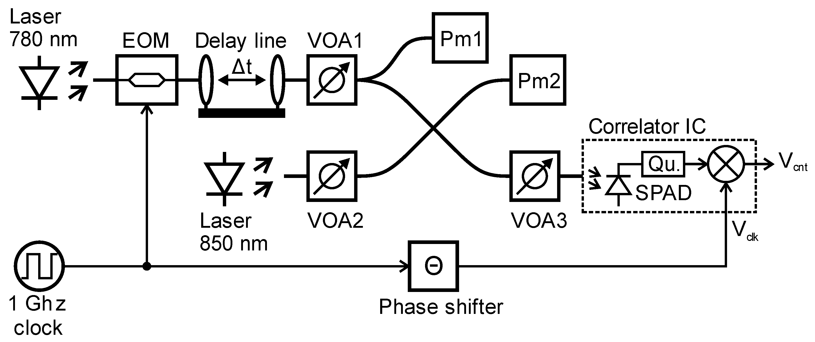
4. Measurement Setup
Figure 5 shows the used measurement setup. After a Thorlabs (Newton, NJ, USA) LPS-PM785-FC laser with a wavelength of 783.4 nm, the light is amplitude modulated with the 1 GHz clock using an iXblue (Besancon, France) NIR-MX800-LN electro-optic modulator (EOM). The following OZ Optics (Ottawa, ON, Canada) ODL-300 adjustable fiber optic delay line allows for the accurate sweeping of the measured delay over a range from 0 ps to 333 ps. The variable optical attenuator VOA1 allows for the sweeping of the optical signal power over a range of 60 dB. After VOA1, a splitter divides the signal for measuring the signal power with power meter Pm1. Background light is generated with an 850 nm laser and adjusted in power with VOA2. For this task, the wavelength of the light source is not critical, as the purpose of this laser is only to trigger SPAD counts, which are not correlated to the signal light as would background light from other light sources or the sun. Signal and background light is combined with a 2 × 2 combiner, where one output is used for power measurement of the combined light intensities, which is performed with a Thorlabs PM100USB power meter (Pm2). The second output of the 2 × 2 combiner is further attenuated with VOA3 and then fed into the integrated SPAD of the proposed single-photon correlator. The coupling ratio of the 2 × 2 combiner and the attenuation of the fiber and VOA3 are carefully measured for both used wavelengths in order to be able to accurately determine the light intensity reaching the SPAD. The quenching circuit generates a pulse for every detected photon. The phase steps
Θ of the reference clock signal
Vclk are generated with a Microchip (Chandler, AZ, USA) SY89295UTG adjustable phase shifter. A National Instruments (Austin, TX, USA) CompactRIO system generates the correlator control signals, controls the phase shifter, and reads the correlation result
Vcnt,end with an NI-9205 16-bit voltage input module. The complete measurement system is controlled by PC and all measurements run fully automated with LabVIEW (15.0). For flexibility reasons, data processing and analysis is done after the measurement in MATLAB (R2022b).
As already explained in
Section 3, in order to prevent asymmetries between up and down counting voltage steps, a balancing by either adjusting
I+ or
I− is necessary. One possibility to measure this asymmetry is using the integrated calibration circuit. Either
I+ or
I− is adjusted until the output voltage of the calibration circuit stays constant; hence, up and down counting voltage steps are identical. Another possibility, which was used for this work, is to measure the asymmetry with the correlator circuit itself. This is done by using either background light photons or SPAD dark counts without modulated signal light. Then, an integration with applied
Vclk is performed with the correlator. As the number of photons or dark counts while
Vclk high and low levels is now identical for a sufficiently long integration time, only an asymmetry between up and down counting voltage steps will cause a change of
Vcnt. As
Vcnt changes according to the direction of the asymmetry,
I+ or
I− can be adjusted until this asymmetry is sufficiently suppressed. As no voltage step drifting was observed over several weeks of measurement, it seems to be sufficient to perform this balancing once.
For a distance measurement, consecutive integrations for the different Vclk phases Θ with integration time Tint are performed. After every integration, Vcnt,end is read out and a correlation triangle is formed. Then, φ is determined with an FFT and d is calculated with Equation (3).
6. Discussion
The purpose of this work is to prove the ability of SPAD-based iTOF with high frequency correlation to achieve sub-100 µm precisions. These good precision results were achieved by the use of a modulation frequency fmod of 1 GHz. Equation (3) shows the relationship between the measured distance and fmod. The high fmod is possible due to the more digital operation of SPADs. The decision between up and down counting can be performed with a fast digital circuit. The achieved precision and linearity in combination with the achieved sensitivity can open up new high-precision measurement applications for TOF sensors, which, so far, depend on more complex interferometric sensors.
Table 1 shows a comparison of high-precision dTOF and iTOF results. To the best of our knowledge, there is no previous work achieving sub-100 µm precisions with SPAD-based integrated TOF. In comparison with integrated dTOF systems, which can achieve precisions in the sub-mm and mm-range, this is an improvement of one order of magnitude. Sub-100 µm precisions were already achieved with PPD-based iTOF. Nonetheless, the SPAD allows much better sensitivities, i.e., requires considerably less light to achieve the same precision.
In contrast to [
11], where digital counters were used, in this work, we use a faster edge-triggered decision circuit in combination with an analog counter. The use of an analog counter promises a higher pixel number especially for large feature size technologies due to smaller area and power consumption. Furthermore, as the analog counter allows for an adjustment of the dynamic range by adjusting
Vstep, it is very flexible in terms of possible integration time in contrast to a digital counter with a strictly limited counting range. Nevertheless, for applications with the need of very long integration times, digital correlators might be favorable as their dynamic range is not limited by electronic noise.
A single pixel prototype was manufactured with an integrated SPAD and quenching circuit. For testing purposes, a quenching circuit with an already proven design [
14,
15] and wide tunability was chosen. It was not optimized for size and consumes a fairly large area (130 µm × 130 µm). Nevertheless, by using area-optimized quenching circuits and smaller feature size technologies this area consumption could be greatly reduced. The same is true for the correlator circuit, which was optimized for flexibility in order to be able to test all parameters and to perform long integrations with many photons. As more than half of the correlator size of 270 µm × 70 µm is used for the counting capacitor
Ccnt, reducing this capacitor size, e.g., by using MOS capacitors or by using smaller application-optimized capacitor values, could save a lot of space. Even a small capacitance of several hundred femtofarads would allow sub-mm precisions. Additionally, a further reduction of
Ccnt might be possible by further reducing
I+/
I−. Nevertheless, an eye must be kept on additional noise due to small currents. In a similar way, shorter
Tpulse values would also allow for the reduction of
Ccnt. In this work,
Tpulse cannot be reduced to values smaller than 4 ns. As the added calibration circuit, which occupies around 30 % of the active correlator area, turned out not to be necessary, it would be possible to remove it. The active area, with SPAD, quenching circuit, and two correlators, measures about 300 × 300 µm
2. Therefore, with the actual prototype in 0.35 µm CMOS, a multi-pixel design would be limited to a low number of pixels for a reasonable cost. Implementing a pixel design by taking into account all the previously mentioned considerations would lead to a drastic shrinking of the occupied area per pixel. Hence, multi-pixel TOF imagers are possible, even with the actual fairly large feature size technology. Switching to smaller feature size technologies would lead to a further pixel size reduction.
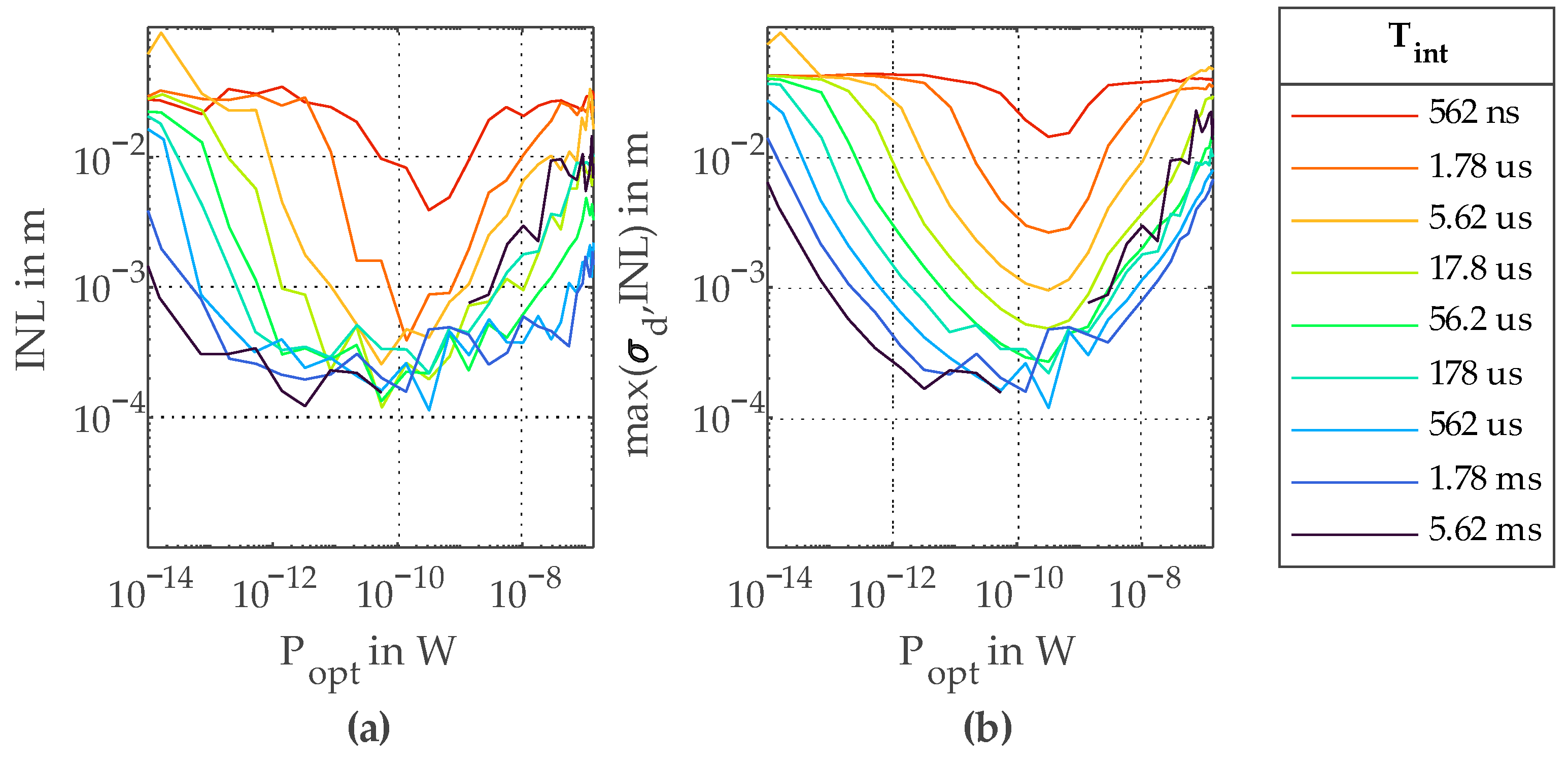
Increasing the dynamic range of the analog counter, for example by increasing
Ccnt or further decreasing
Vstep, would allow for longer integration times. Extrapolating the logarithmic relationship in
Figure 7 allows an estimation of achievable measurement precisions. Achieving precisions of 10 µm or even better might be possible with measurement times of less than a second. Nevertheless, it would be hard to combine such precisions with a high pixel number.
As in this work, the different phase steps were measured consecutively, the total measurement time could be drastically reduced by adding parallel correlators for every phase step. Hence, a simultaneous measurement of all phase steps would be possible.
One major drawback of the actual measurements with a simple square wave modulation is the very limited unambiguous range, which for the used
fmod of 1 GHz is just 15 cm. One solution for this problem would be using two modulation frequencies [
16]. Another solution is using orthogonal codes for the signal modulation [
17,
18,
19]. This would bring the additional feature of high immunity to interferers. By using orthogonal coding, the unambiguous range could be simply adjusted with the code length, hence allowing for the combination of a high frequency measurement with a high unambiguous range. In this case, the maximum measurement range would be limited by the sensitivity of the SPAD. Depending on the optics and background light conditions, with an eye-safe laser, a measurement range of at least several 10s of meters should be easily possible. Nevertheless, for applications with high background light levels, narrow laser line filters might be necessary to prevent saturation of the SPAD.


