
Elucidating the Conducting Mechanisms in a Flexible Piezoresistive Pressure Sensor Using Reduced Graphene Oxide Film in Silicone Elastomer


Abstract
1. Introduction
2. Results and Discussion
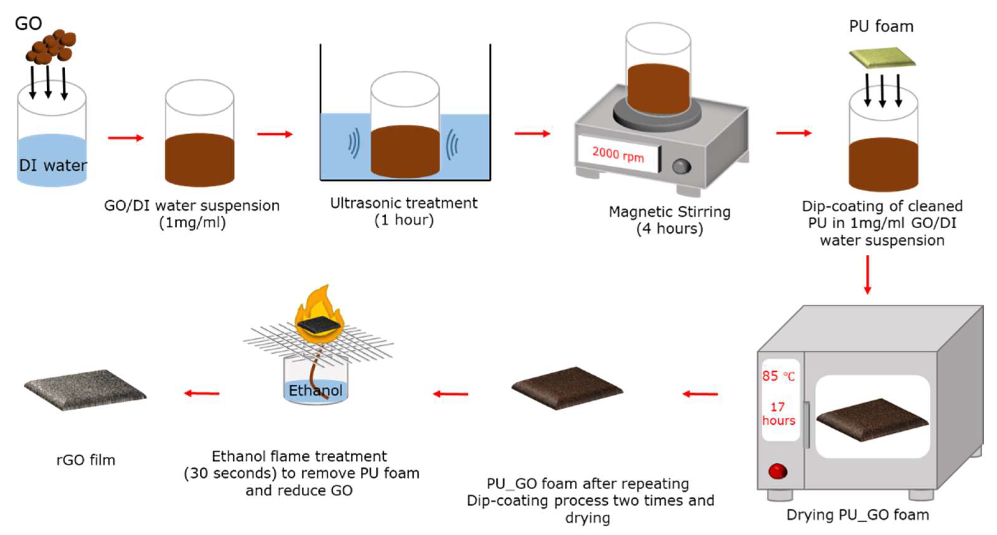
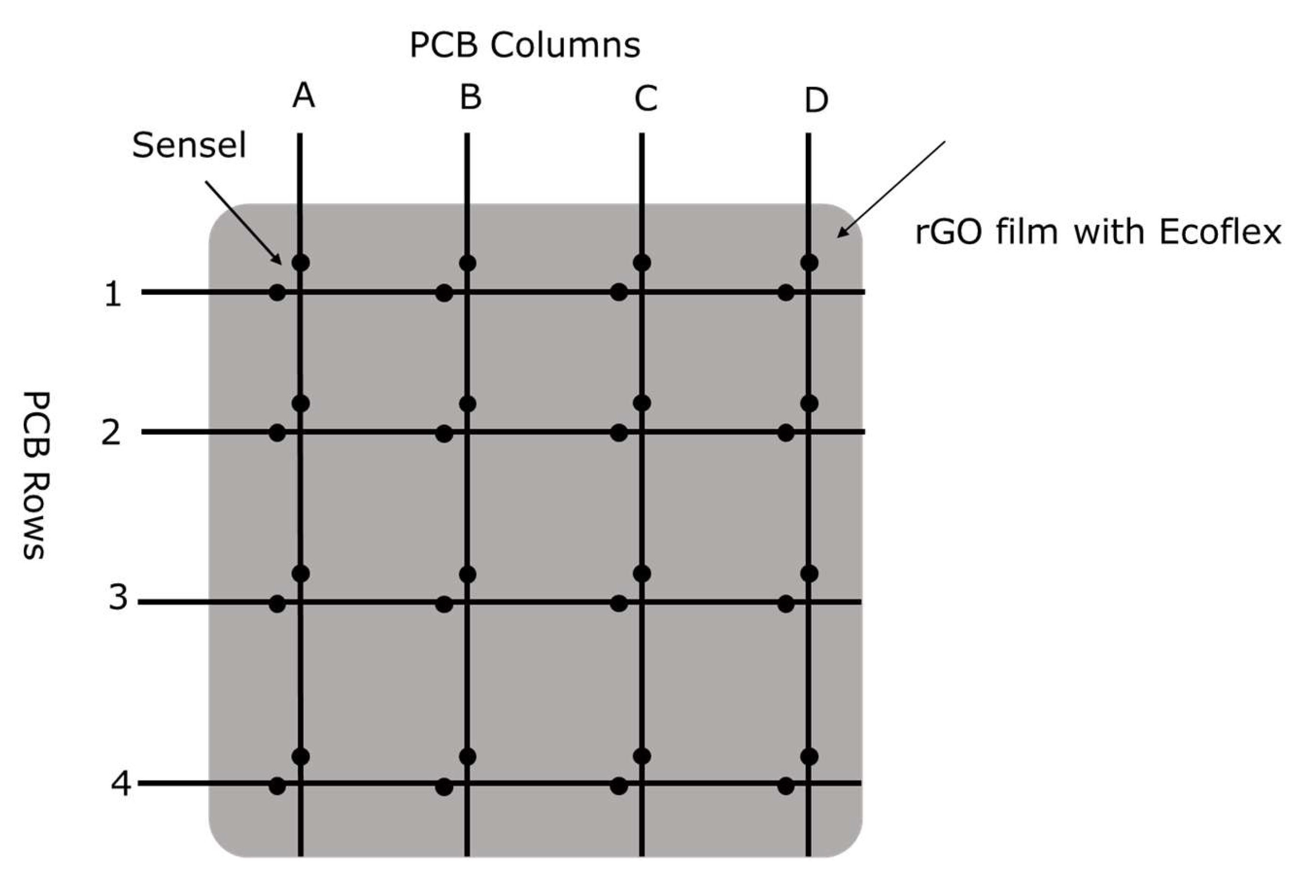
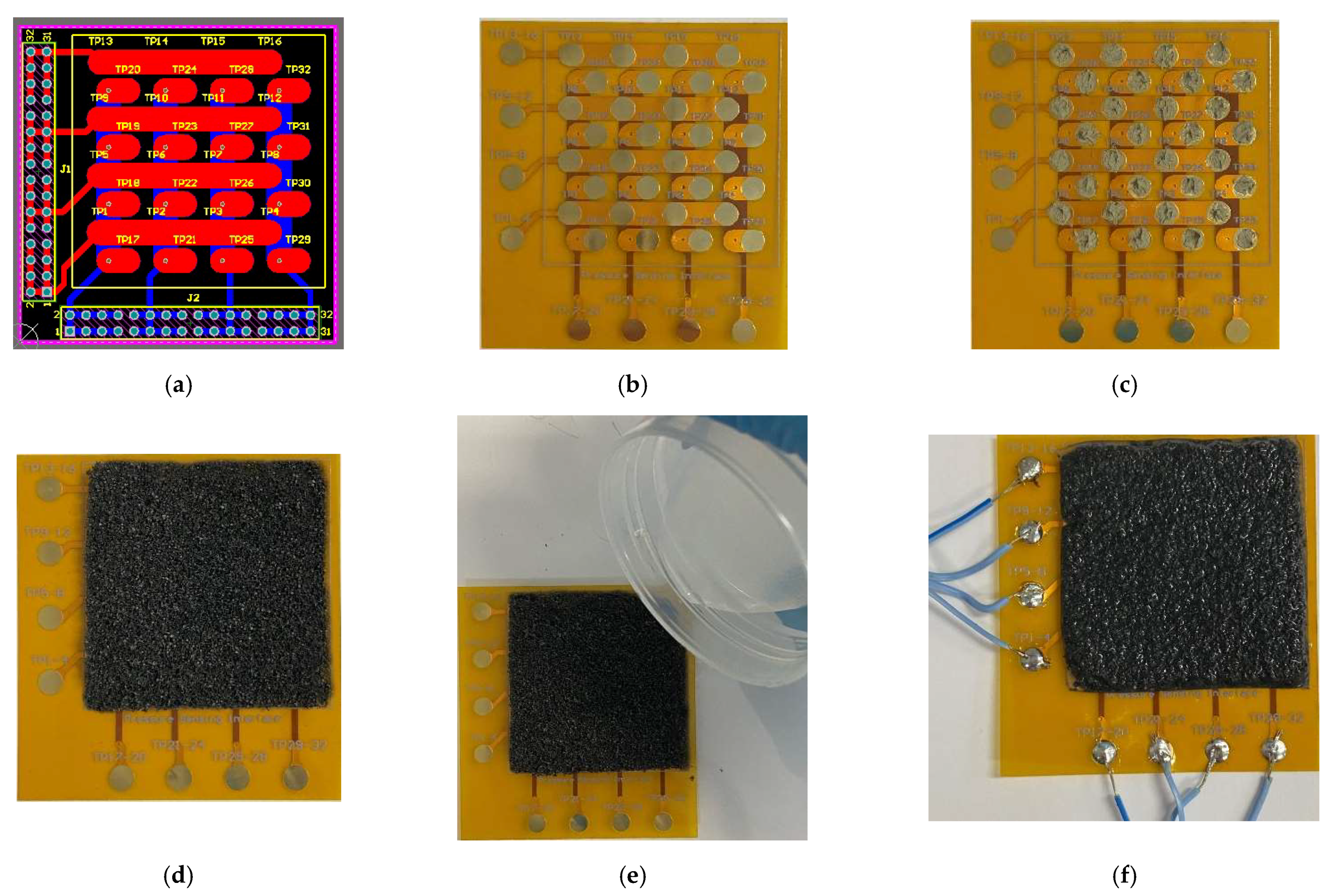
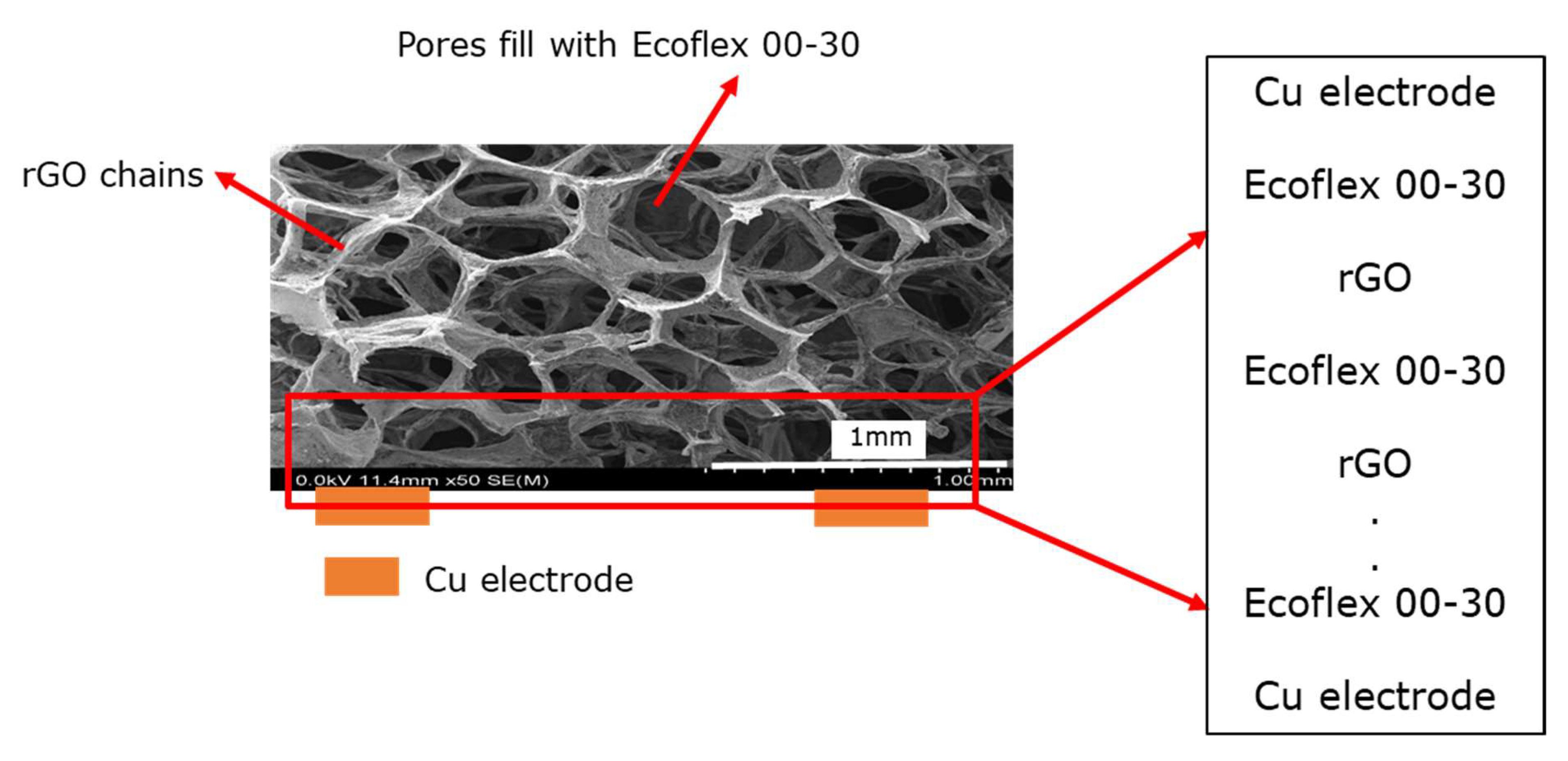
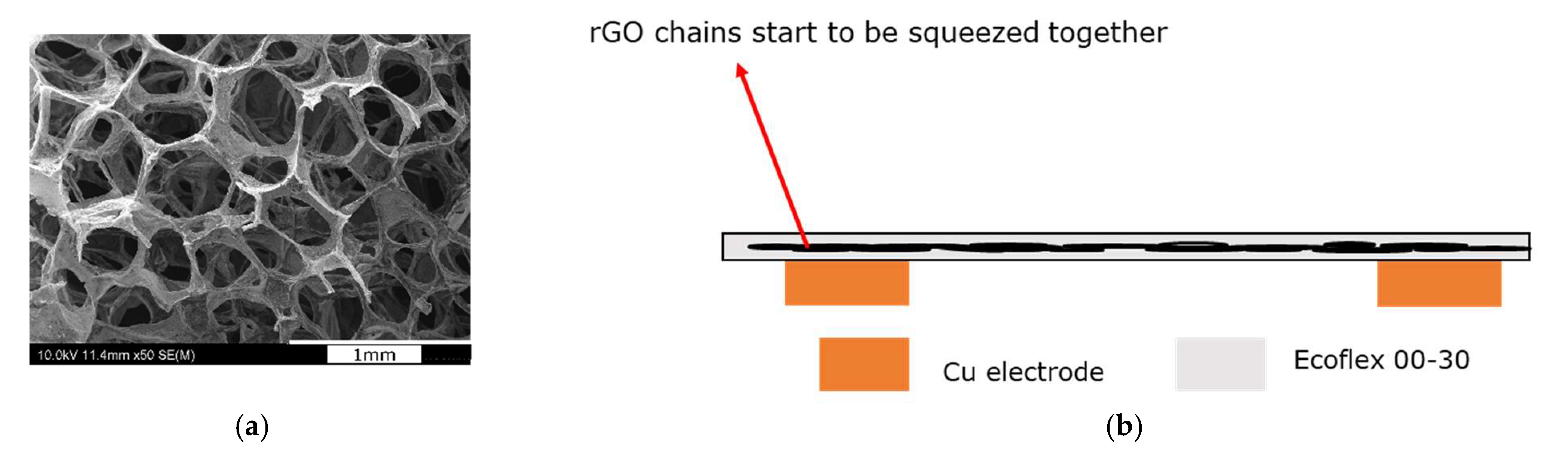
2.1. Fabrication Method
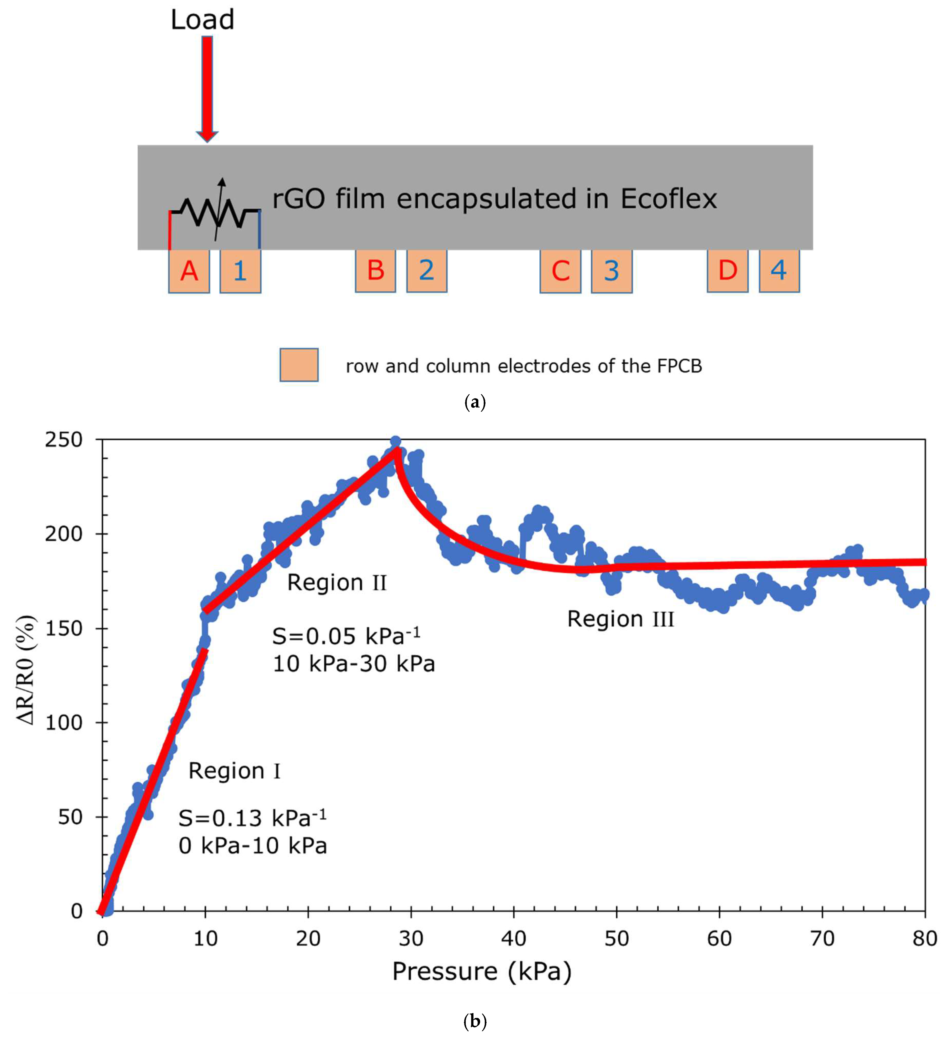
2.2. Sensitivity of the rGO-Based Flexible Pressure Sensor
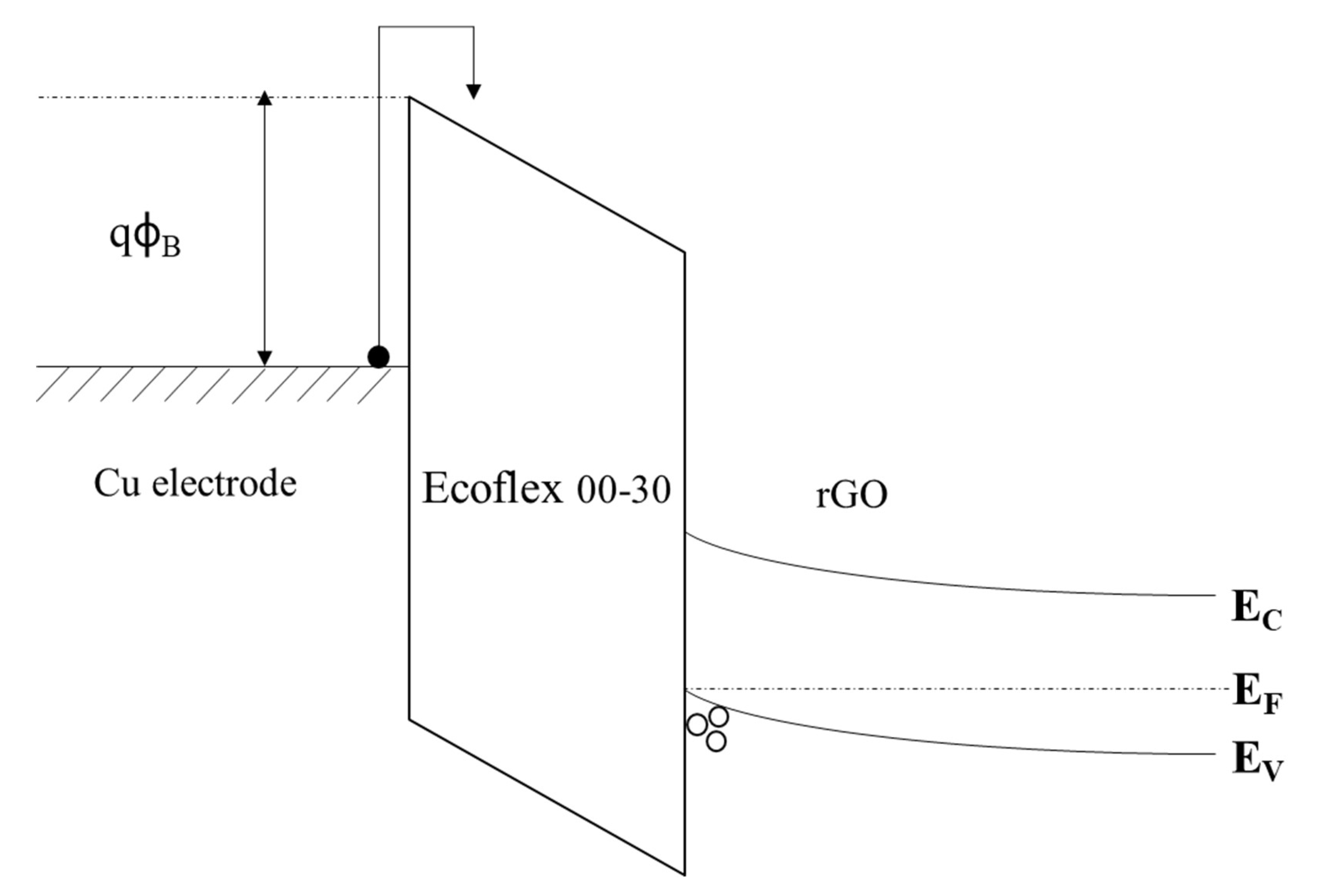
2.3. Conducting Mechanisms of the rGO-Based Flexible Pressure Sensor

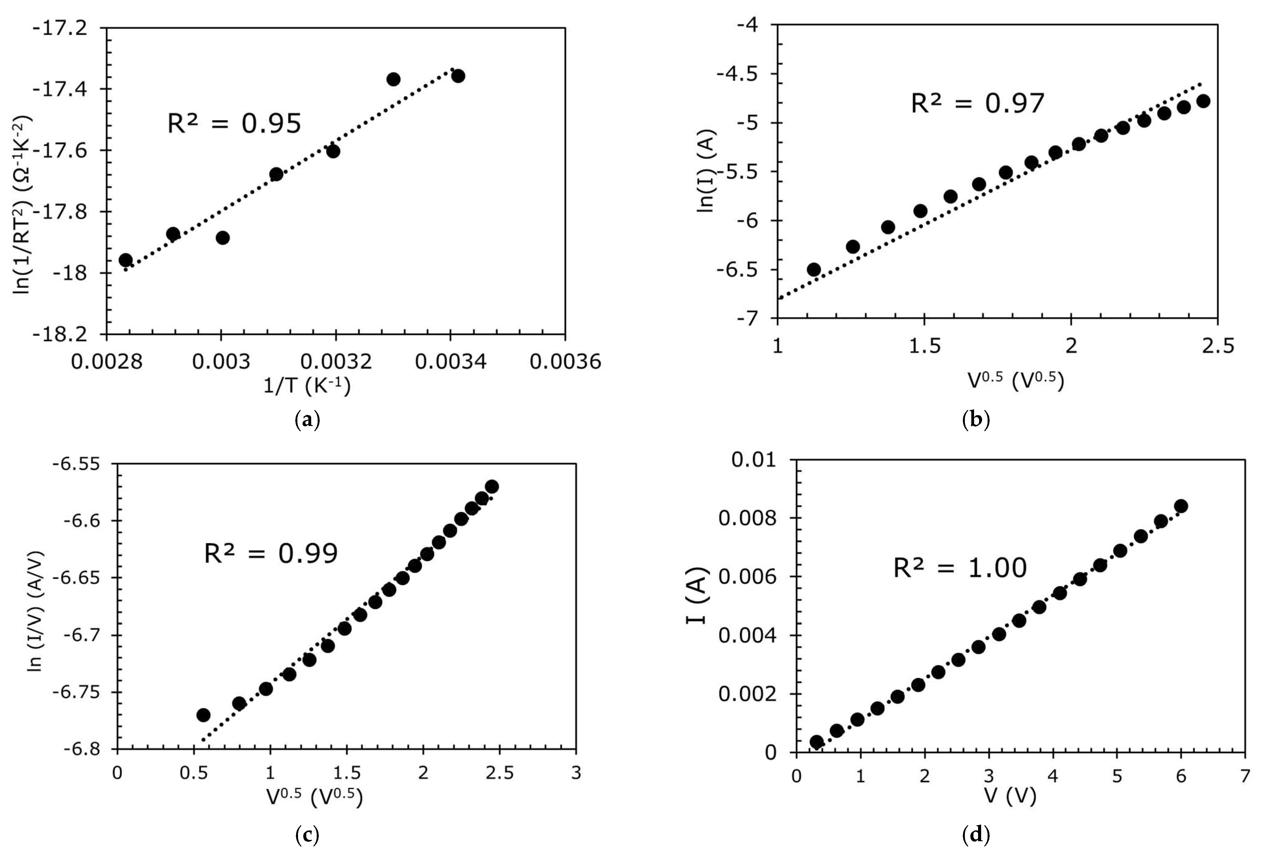
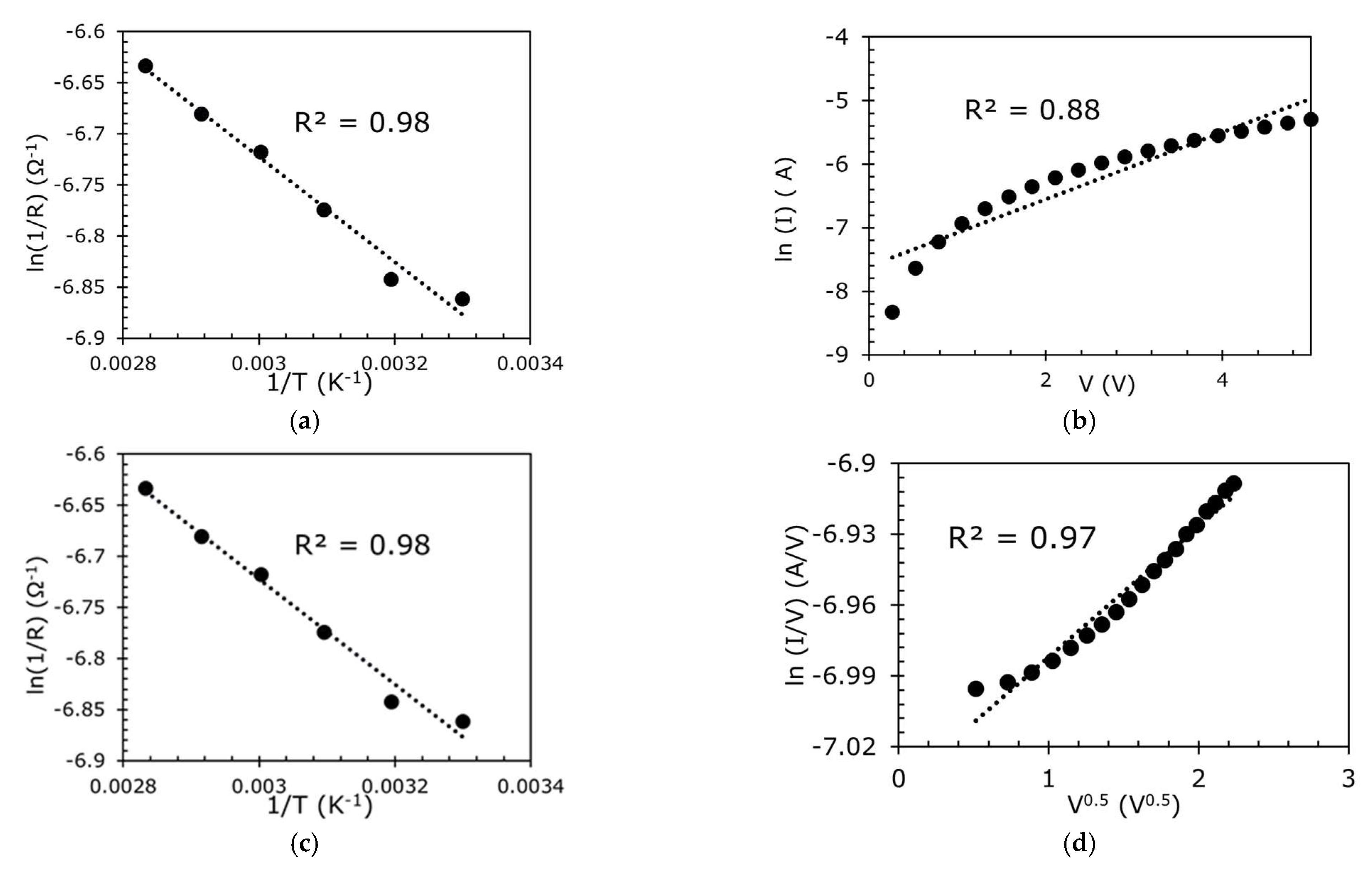
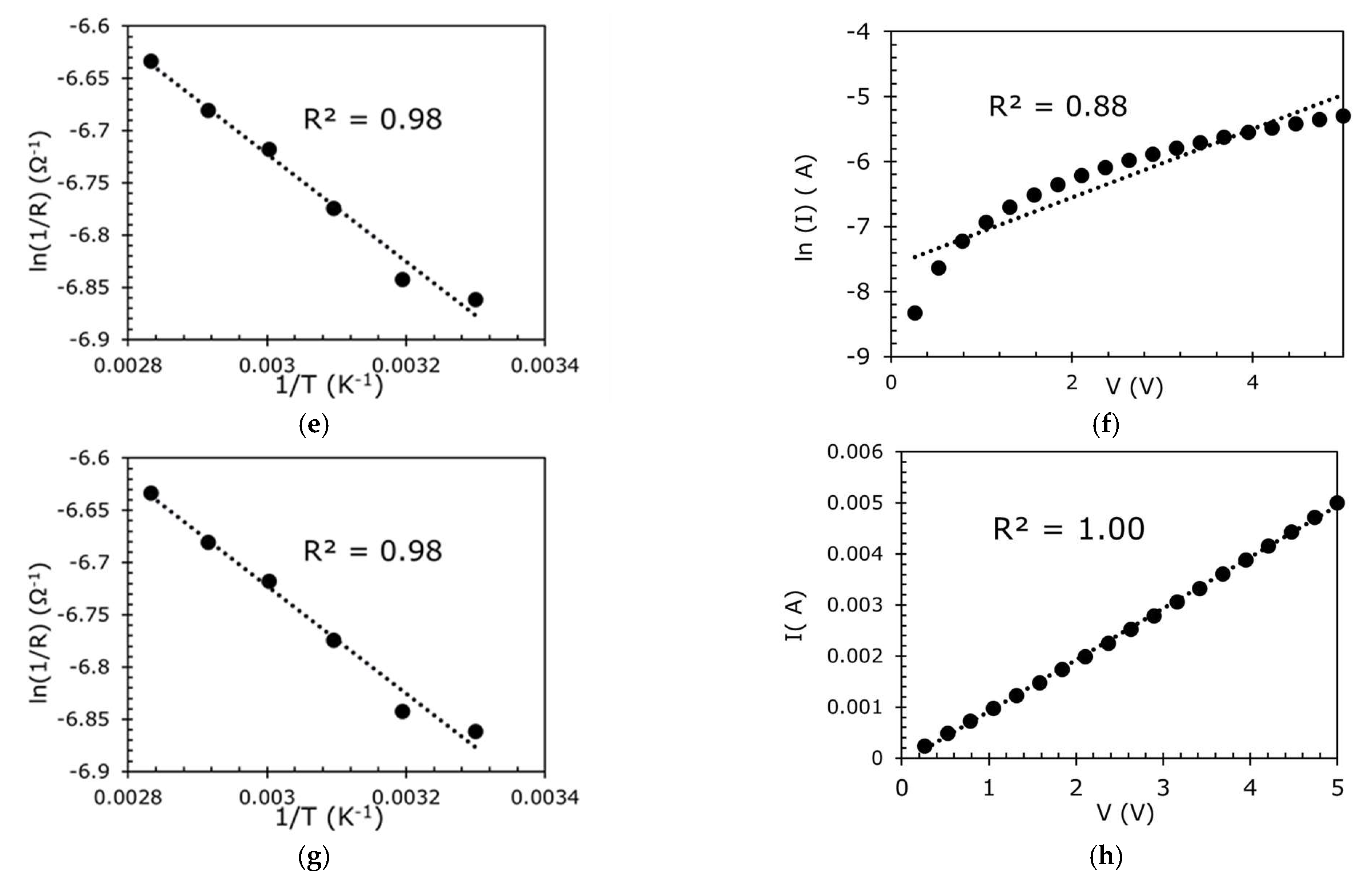
| Conduction Mechanisms | |
|---|---|
| Electrode-Limited Conduction Mechanism | Bulk-Limited Conduction Mechanism |
|
|
|
|
|
|
|
|
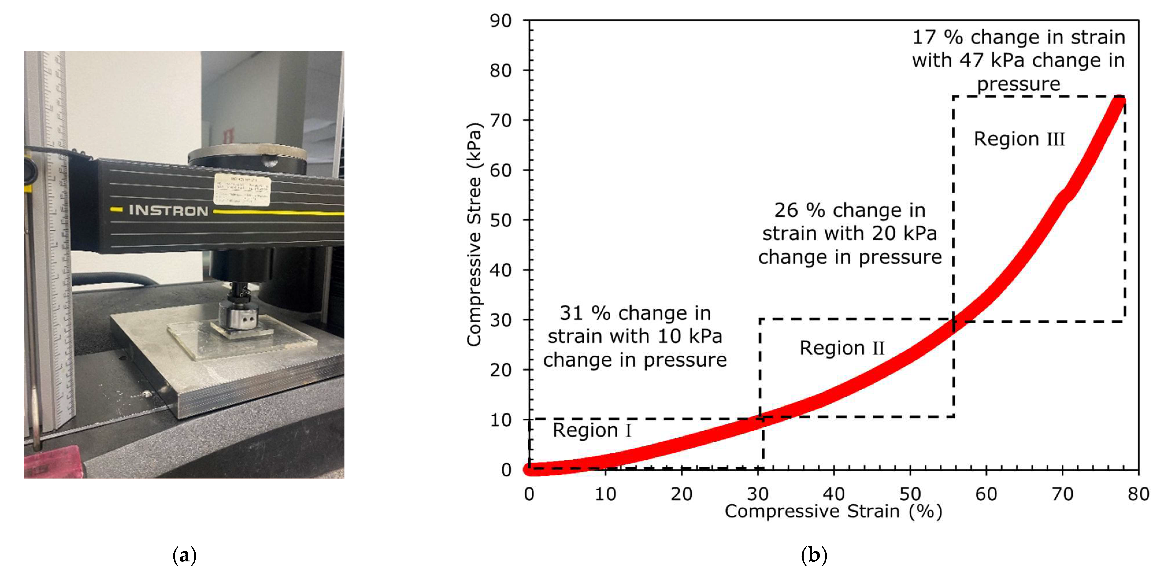
2.3.1. Region I: Conduction Mechanism of the Sensor at Low Pressure (0–10 kPa)
2.3.2. Region II: Conduction Mechanism of the Sensor at Medium Pressure (10–30 kPa)
2.3.3. Region III: Conduction Mechanism of the Sensor at High Pressure > 30 kPa
3. Conclusions
Author Contributions
Funding
Institutional Review Board Statement
Informed Consent Statement
Data Availability Statement
Conflicts of Interest
References
- Pang, Y.; Tian, H.; Tao, L.; Li, Y.; Wang, X.; Deng, N.; Yang, Y.; Ren, T.-L. Flexible, highly sensitive, and wearable pressure and strain sensors with graphene porous network structure. ACS Appl. Mater. Interfaces 2016, 8, 26458–26462. [Google Scholar] [CrossRef]
- Luo, S.; Yang, J.; Song, X.; Zhou, X.; Yu, L.; Sun, T.; Yu, C.; Huang, D.; Du, C.; Wei, D. Tunable-sensitivity flexible pressure sensor based on graphene transparent electrode. Solid State Electron. 2018, 145, 29–33. [Google Scholar] [CrossRef]
- Ding, Y.; Xu, T.; Onyilagha, O.; Fong, H.; Zhu, Z. Recent advances in flexible and wearable pressure sensors based on piezoresistive 3D monolithic conductive sponges. ACS Appl. Mater. Interfaces 2019, 11, 6685–6704. [Google Scholar] [CrossRef]
- Wang, B.; Shi, T.; Zhang, Y.; Chen, C.; Li, Q.; Fan, Y. Lignin-based highly sensitive flexible pressure sensor for wearable electronics. J. Mater. Chem. C 2018, 6, 6423–6428. [Google Scholar] [CrossRef]
- Lou, Z.; Chen, S.; Wang, L.; Jiang, K.; Shen, G. An ultra-sensitive and rapid response speed graphene pressure sensors for electronic skin and health monitoring. Nano Energy 2016, 23, 7–14. [Google Scholar] [CrossRef]
- Yao, H.B.; Ge, J.; Wang, C.F.; Wang, X.; Hu, W.; Zheng, Z.J.; Ni, Y.; Yu, S.H. A flexible and highly pressure-sensitive graphene–polyurethane sponge based on fractured microstructure design. Adv. Mater. 2013, 25, 6692–6698. [Google Scholar] [CrossRef]
- Ai, Y.; Hsu, T.H.; Wu, D.C.; Lee, L.; Chen, J.-H.; Chen, Y.-Z.; Wu, S.-C.; Wu, C.; Wang, Z.M.; Chueh, Y.-L. An ultrasensitive flexible pressure sensor for multimodal wearable electronic skins based on large-scale polystyrene ball@ reduced graphene-oxide core–shell nanoparticles. J. Mater. Chem. C 2018, 6, 5514–5520. [Google Scholar] [CrossRef]
- Liu, W.; Liu, N.; Yue, Y.; Rao, J.; Luo, C.; Zhang, H.; Yang, C.; Su, J.; Liu, Z.; Gao, Y. A flexible and highly sensitive pressure sensor based on elastic carbon foam. J. Mater. Chem. C 2018, 6, 1451–1458. [Google Scholar] [CrossRef]
- Yan, C.; Wang, J.; Kang, W.; Cui, M.; Wang, X.; Foo, C.Y.; Chee, K.J.; Lee, P.S. Highly stretchable piezoresistive graphene–nanocellulose nanopaper for strain sensors. Adv. Mater. 2014, 26, 2022–2027. [Google Scholar] [CrossRef]
- Enser, H.; Sell, J.K.; Schatzl-Linder, M.; Strauß, B.; Hilber, W.; Jakoby, B. Hysteresis and material effects of printed strain gauges embedded in organic coatings. Proceedings 2017, 1, 624. [Google Scholar] [CrossRef]
- Ruth, S.R.A.; Feig, V.R.; Tran, H.; Bao, Z. Microengineering pressure sensor active layers for improved performance. Adv. Funct. Mater. 2020, 30, 2003491. [Google Scholar] [CrossRef]
- Mishra, R.B.; El-Atab, N.; Hussain, A.M.; Hussain, M.M. Recent progress on flexible capacitive pressure sensors: From design and materials to applications. Adv. Mater. Technol. 2021, 6, 2001023. [Google Scholar] [CrossRef]
- Mannsfeld, S.C.; Tee, B.C.; Stoltenberg, R.M.; Chen, C.V.; Barman, S.; Muir, B.V.; Sokolov, A.N.; Reese, C.; Bao, Z. Highly sensitive flexible pressure sensors with microstructured rubber dielectric layers. Nat. Mater. 2010, 9, 859–864. [Google Scholar] [CrossRef]
- Wong, R.D.P.; Posner, J.D.; Santos, V.J. Flexible microfluidic normal force sensor skin for tactile feedback. Sens. Actuators A 2012, 179, 62–69. [Google Scholar] [CrossRef]
- Duan, Y.; He, S.; Wu, J.; Su, B.; Wang, Y. Recent progress in flexible pressure sensor arrays. Nanomaterials 2022, 12, 2495. [Google Scholar] [CrossRef]
- Garcia, C.; Trendafilova, I.; de Villoria, R.G.; del Rio, J.S. Self-powered pressure sensor based on the triboelectric effect and its analysis using dynamic mechanical analysis. Nano Energy 2018, 50, 401–409. [Google Scholar] [CrossRef]
- Shi, Z.; Meng, L.; Shi, X.; Li, H.; Zhang, J.; Sun, Q.; Liu, X.; Chen, J.; Liu, S. Morphological engineering of sensing materials for flexible pressure sensors and artificial intelligence applications. Nano Micro Lett. 2022, 14, 1–48. [Google Scholar] [CrossRef]
- Vivekananthan, V.; Chandrasekhar, A.; Alluri, N.R.; Purusothaman, Y.; Kim, S.-J. A highly reliable, impervious and sustainable triboelectric nanogenerator as a zero-power consuming active pressure sensor. Nanoscale Adv. 2020, 2, 746–754. [Google Scholar] [CrossRef]
- Ji, B.; Zhou, Q.; Hu, B.; Zhong, J.; Zhou, J.; Zhou, B. Bio-inspired hybrid dielectric for capacitive and triboelectric tactile sensors with high sensitivity and ultrawide linearity range. Adv. Mater. 2021, 33, 2100859. [Google Scholar] [CrossRef]
- Tao, K.; Chen, Z.; Yu, J.; Zeng, H.; Wu, J.; Wu, Z.; Jia, Q.; Li, P.; Fu, Y.; Chang, H. Ultra-Sensitive, Deformable, and Transparent Triboelectric Tactile Sensor Based on Micro-Pyramid Patterned Ionic Hydrogel for Interactive Human–Machine Interfaces. Adv. Sci. 2022, 9, 2104168. [Google Scholar] [CrossRef]
- Su, M.; Li, P.; Liu, X.; Wei, D.; Yang, J. Textile-Based Flexible Capacitive Pressure Sensors: A Review. Nanomaterials 2022, 12, 1495. [Google Scholar] [CrossRef]
- Zhang, P.; Chen, Y.; Guo, Z.H.; Guo, W.; Pu, X.; Wang, Z.L. Stretchable, transparent, and thermally stable triboelectric nanogenerators based on solvent-free ion-conducting elastomer electrodes. Adv. Funct. Mater. 2020, 30, 1909252. [Google Scholar] [CrossRef]
- Jiang, Y.; Dong, K.; Li, X.; An, J.; Wu, D.; Peng, X.; Yi, J.; Ning, C.; Cheng, R.; Yu, P. Stretchable, washable, and ultrathin triboelectric nanogenerators as skin-like highly sensitive self-powered haptic sensors. Adv. Funct. Mater. 2021, 31, 2005584. [Google Scholar] [CrossRef]
- Chen, S.; Wu, N.; Lin, S.; Duan, J.; Xu, Z.; Pan, Y.; Zhang, H.; Xu, Z.; Huang, L.; Hu, B. Hierarchical elastomer tuned self-powered pressure sensor for wearable multifunctional cardiovascular electronics. Nano Energy 2020, 70, 104460. [Google Scholar] [CrossRef]
- Zhong, W.; Ding, X.; Li, W.; Shen, C.; Yadav, A.; Chen, Y.; Bao, M.; Jiang, H.; Wang, D. Facile fabrication of conductive graphene/polyurethane foam composite and its application on flexible piezoresistive sensors. Polymers 2019, 11, 1289. [Google Scholar] [CrossRef]
- Xu, D.; Wang, Q.; Feng, D.; Liu, P. Facile fabrication of multifunctional poly (ethylene-co-octene)/carbon nanotube foams based on tunable conductive network. Ind. Eng. Chem. Res. 2020, 59, 1934–1943. [Google Scholar] [CrossRef]
- Cheng, H.; Wang, B.; Yang, K.; Wang, C. A low-cost piezoresistive pressure sensor with a wide strain range–featuring polyurethane sponge@ poly (vinyl alcohol)/sulfuric gel electrolyte. J. Mater. Chem. C 2021, 9, 1014–1024. [Google Scholar] [CrossRef]
- Fiorillo, A.S.; Critello, C.D.; Pullano, S.A. Theory, technology and applications of piezoresistive sensors: A review. Sens. Actuators A 2018, 281, 156–175. [Google Scholar] [CrossRef]
- Zheng, Q.; Lee, J.-h.; Shen, X.; Chen, X.; Kim, J.-K. Graphene-based wearable piezoresistive physical sensors. Mater. Today 2020, 36, 158–179. [Google Scholar] [CrossRef]
- Zhu, Y.; Hartel, M.C.; Yu, N.; Garrido, P.R.; Kim, S.; Lee, J.; Bandaru, P.; Guan, S.; Lin, H.; Emaminejad, S. Epidermis-Inspired Wearable Piezoresistive Pressure Sensors Using Reduced Graphene Oxide Self-Wrapped Copper Nanowire Networks. Small Methods 2022, 6, 2100900. [Google Scholar] [CrossRef]
- Kanoun, O.; Bouhamed, A.; Ramalingame, R.; Bautista-Quijano, J.R.; Rajendran, D.; Al-Hamry, A. Review on conductive polymer/CNTs nanocomposites based flexible and stretchable strain and pressure sensors. Sensors 2021, 21, 341. [Google Scholar] [CrossRef]
- Gilanizadehdizaj, G.; Aw, K.C.; Stringer, J.; Bhattacharyya, D. Facile fabrication of flexible piezoresistive pressure sensor array using reduced graphene oxide foam and silicone elastomer. Sens. Actuators A 2022, 340, 113549. [Google Scholar] [CrossRef]
- Eom, S.; Lim, S. Stretchable complementary split ring resonator (CSRR)-based radio frequency (RF) sensor for strain direction and level detection. Sensors 2016, 16, 1667. [Google Scholar] [CrossRef]
- Chiu, F.-C. A review on conduction mechanisms in dielectric films. Adv. Mater. Sci. Eng. 2014, 2014, 2014. [Google Scholar] [CrossRef]
- Lamb, D.R. Electrical Conduction Mechanisms in Thin Insulating Films; Methuen: London, UK, 1967. [Google Scholar]
- Hesto, P. The nature of electronic conduction in thin insulating layers. In Instabilities in Silicon Devices; North-Holland: Amsterdam, The Netherlands, 1986; Volume 1, pp. 276–277. [Google Scholar]
- Kao, K.C. Dielectric Phenomena in Solids; Elsevier: Amsterdam, The Netherlands, 2004. [Google Scholar]
- Hamann, C.; Burghardt, H.; Frauenheim, T. Electrical Conduction Mechanisms in Solids; Vch Pub: Berlin, Germany, 1988. [Google Scholar]
- O’Dwyer, J.J. The Theory of Electrical Conduction and Breakdown in Solid Dielectrics; Clarendon Press: Oxford, UK, 1973. [Google Scholar]
- Mott, N.F.; Davis, E.A. Electronic Processes in Non-Crystalline Materials; Oxford University Press: Oxford, UK, 2012. [Google Scholar]
- Chiu, F.-C.; Lai, C.-M. Optical and electrical characterizations of cerium oxide thin films. J. Phys. D Appl. Phys. 2010, 43, 075104. [Google Scholar] [CrossRef]
- Sze, S.M.; Li, Y.; Ng, K.K. Physics of Semiconductor Devices; John Wiley & Sons: Hoboken, NJ, USA, 2021. [Google Scholar]
- Chiu, F.-C. Interface characterization and carrier transportation in metal/Hf O 2/silicon structure. J. Appl. Phys. 2006, 100, 114102. [Google Scholar] [CrossRef]
- Chiu, F.-C.; Lee, C.-Y.; Pan, T.-M. Current conduction mechanisms in Pr2O3/oxynitride laminated gate dielectrics. J. Appl. Phys. 2009, 105, 074103. [Google Scholar] [CrossRef]
- Yeo, Y.-C.; King, T.-J.; Hu, C. Direct tunneling leakage current and scalability of alternative gate dielectrics. Appl. Phys. Lett. 2002, 81, 2091–2093. [Google Scholar] [CrossRef]
- Lee, J.; Chiu, F.; Juan, P. The application of high-dielectric-constant and ferroelectric thin films in integrated circuit technology. In Handbook of Nanoceramics and Their Based Nanodevices; American Scientific Publishers: Valencia, CA, USA, 2009; Volume 4, p. 159. [Google Scholar]
- Wang, L.; Baumgartner, A.; Makk, P.; Zihlmann, S.; Varghese, B.S.; Indolese, D.I.; Watanabe, K.; Taniguchi, T.; Schönenberger, C. Global strain-induced scalar potential in graphene devices. Commun. Phys. 2021, 4, 1–6. [Google Scholar] [CrossRef]


| Electrode-Limited Conduction Mechanism | Fowler–Nordheim (F–N) Tunneling | Direct Tunneling | Thermionic Field Emission | Schottky/thermionic emission |
| I–V plot | 0.84 | N.A. | 0.80 | 0.97 |
| R–T plot | N.A. | N.A. | 0.85 | 0.95 |
| Bulk-limited conduction mechanism | Poole–Frenkel (P–F) emission | Hopping conduction | Ohmic conduction | Ionic conduction |
| I–V plot | 0.99 | 0.88 | 1 | 0.88 |
| R–T plot | 0.77 | 0.77 | 0.77 | 0.77 |
Disclaimer/Publisher’s Note: The statements, opinions and data contained in all publications are solely those of the individual author(s) and contributor(s) and not of MDPI and/or the editor(s). MDPI and/or the editor(s) disclaim responsibility for any injury to people or property resulting from any ideas, methods, instructions or products referred to in the content. |
© 2023 by the authors. Licensee MDPI, Basel, Switzerland. This article is an open access article distributed under the terms and conditions of the Creative Commons Attribution (CC BY) license (https://creativecommons.org/licenses/by/4.0/).
Share and Cite
Gilanizadehdizaj, G.; Bhattacharyya, D.; Stringer, J.; Aw, K. Elucidating the Conducting Mechanisms in a Flexible Piezoresistive Pressure Sensor Using Reduced Graphene Oxide Film in Silicone Elastomer. Sensors 2023, 23, 2443. https://doi.org/10.3390/s23052443
Gilanizadehdizaj G, Bhattacharyya D, Stringer J, Aw K. Elucidating the Conducting Mechanisms in a Flexible Piezoresistive Pressure Sensor Using Reduced Graphene Oxide Film in Silicone Elastomer. Sensors. 2023; 23(5):2443. https://doi.org/10.3390/s23052443
Chicago/Turabian StyleGilanizadehdizaj, Golezar, Debes Bhattacharyya, Jonathan Stringer, and Kean Aw. 2023. "Elucidating the Conducting Mechanisms in a Flexible Piezoresistive Pressure Sensor Using Reduced Graphene Oxide Film in Silicone Elastomer" Sensors 23, no. 5: 2443. https://doi.org/10.3390/s23052443
APA StyleGilanizadehdizaj, G., Bhattacharyya, D., Stringer, J., & Aw, K. (2023). Elucidating the Conducting Mechanisms in a Flexible Piezoresistive Pressure Sensor Using Reduced Graphene Oxide Film in Silicone Elastomer. Sensors, 23(5), 2443. https://doi.org/10.3390/s23052443