Article

Shadow Filters Using Multiple-Input Differential Difference Transconductance Amplifiers

1
Department of Telecommunications Engineering, School of Engineering, King Mongkut’s Institute of Technology Ladkrabang, Bangkok 10520, Thailand
2
Department of Microelectronics, Brno University of Technology, Technická 10, 601 90 Brno, Czech Republic
3
Faculty of Biomedical Engineering, Czech Technical University in Prague, nám. Sítná 3105, 272 01 Kladno, Czech Republic
4
Department of Electrical Engineering, University of Defence, Kounicova 65, 662 10 Brno, Czech Republic
5
Department of Electrical Engineering, Czestochowa University of Technology, 42-201 Czestochowa, Poland
*
Author to whom correspondence should be addressed.
Sensors 2023, 23(3), 1526; https://doi.org/10.3390/s23031526
Submission received: 27 December 2022 / Revised: 9 January 2023 / Accepted: 25 January 2023 / Published: 30 January 2023
(This article belongs to the Section Electronic Sensors)

Abstract

:
This paper presents new voltage-mode shadow filters employing a low-power multiple-input differential difference transconductance amplifier (MI-DDTA). This device provides multiple-input voltage-mode arithmetic operation capability, electronic tuning ability, high-input and low-output impedances. Therefore, the proposed shadow filters offer circuit simplicity, minimum number of active and passive elements, electronic control of the natural frequency and the quality factor, and high-input and low-output impedances. The proposed MI-DDTA can work with supply voltage of ±0.5 V and consumes 9.94 μW of power. The MI-DDTA and shadow filters have been designed and simulated with the SPICE program using 0.18 μm CMOS process parameters to validate the functionality and workability of the new circuits.

1. Introduction

The universal filters are the systems that can realize several filtering functions into the same topology such as low-pass (LP), high-pass (HP), band-pass (BP), band-stop (BS), and all-pass (AP) filters, usually with second-order transfer functions [1,2,3,4,5]. These second-order filters can be applied for three-way high-fidelity loud-speakers, phase-locked loops, and high-order filters [6,7,8]. The filters with orthogonal control of the natural frequency and the quality factor are usually required because it is easy to design the required operating frequency and the required quality factor.
The shadow filter was first introduced in [9]. It consists of a conventional universal filter with LP and BP outputs, summing circuit, and an external amplifier. The output signal of the LP filter is amplified by the external amplifier and fed back to the summing circuit at the input of the universal filter. The adjustable gain of the amplifier can be used to modify the natural frequency and the quality factor of the universal filters, which is valuable for trimming the parameters of filters when non-ideal effects are occurred. The concept of the shadow filter in [9] was developed next to obtain both modification of the natural frequency and the quality factor with an external amplifier [10].
There are many shadow filters (also known as frequency-agile filters) realized using variant active elements available in the literature [11,12,13,14,15,16,17,18,19,20]. In [11,12,13,14,15,16,17,18], current-mode (CM) shadow filters have been reported whereas in [19,20,21,22,23,24,25,26,27,28,29,30] voltage-mode (VM) shadow filters have been introduced. This paper is focused on the VM filters which offer high-input and low-output impedances, electronic tuning ability, and use grounded passive components. The VM shadow filters using active elements such as operational trans-resistance amplifier (OTRA) [19], current-feedback operational amplifier (CFOA) [20,21], and differential-difference current conveyor (DDCC) [22] have been previously introduced in literature. However, the circuits in [19,20,21,22] don’t provide an electronic tuning ability of the natural frequency and the quality factor. The shadow filters employing voltage differencing transconductance amplifier (VDTA) [23,24,25,26,27], voltage differencing gain amplifier (VDGA) [28], voltage differencing differential difference amplifier (VDDDA) [29], and operational transconductance amplifier (OTA) [30] offer an electronic tuning ability and high-input impedance, which is advantageous for VM circuits. However, these active filters were supplied with relatively high voltages, namely, ±0.9 V in [23,29], ±1 V in [24,25,27], ±1.5 V in [26], and ±1.8 V in [30].
In this paper a new voltage-mode shadow filters using low-voltage and low-power multiple-input differential difference transconductance amplifiers (MI-DDTA) have been proposed. The MI-DDTA offers multiple-input addition and subtraction of voltages, which is possible by using the multiple-input gate-driven MOS transistor (MIGD MOST) technique [31,32,33,34,35,36]. The proposed filters offer high-input and low output impedance which is required for cascading in voltage-mode circuits. The natural frequency and the quality factor can be controlled electronically. The proposed circuits can work with ±0.5 V supply and they have been designed and simulated with SPICE, using 0.18 μm CMOS process parameters to verify the functionality and workability of the new circuits.
It is worth noting that the DDTAs using multiple-input bulk-driven MOST technique have been proposed already in [37,38,39]. The DDTAs in [37,38] use a 0.5 V of supply voltage, and the DDTA in [39] uses a 0.3 V of supply voltage. These DDTAs consume ultra-low power in the range of nano watt; however, they are suitable for applications operating with limited bandwidth in the range of a few hundred Hz like applications in biomedical systems.

2. Proposed Circuit

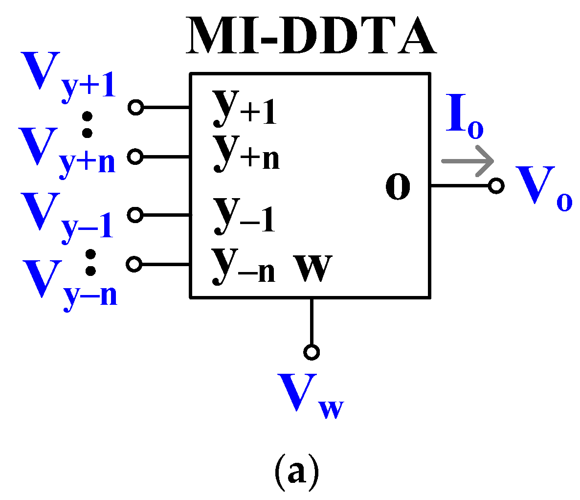
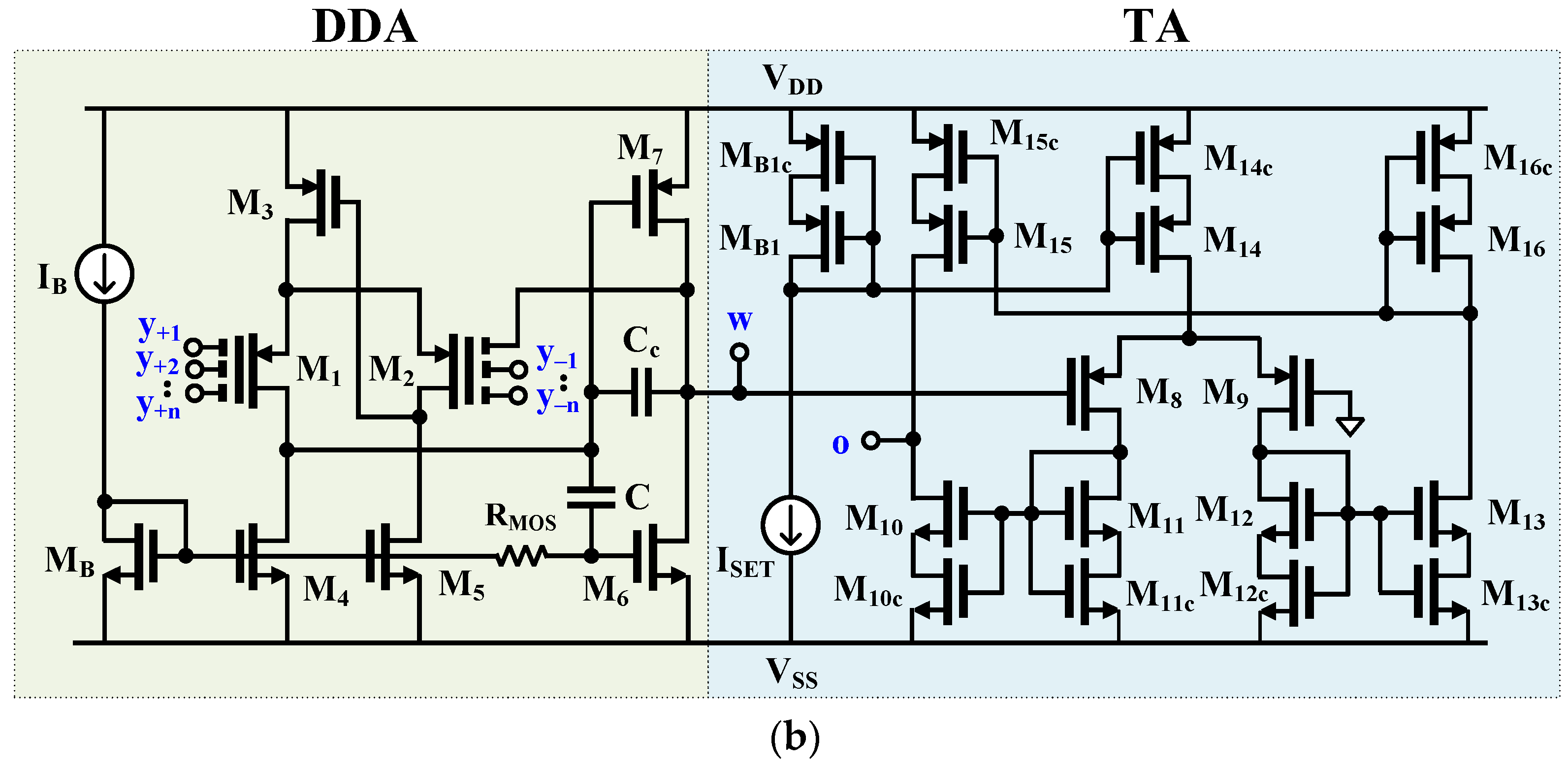
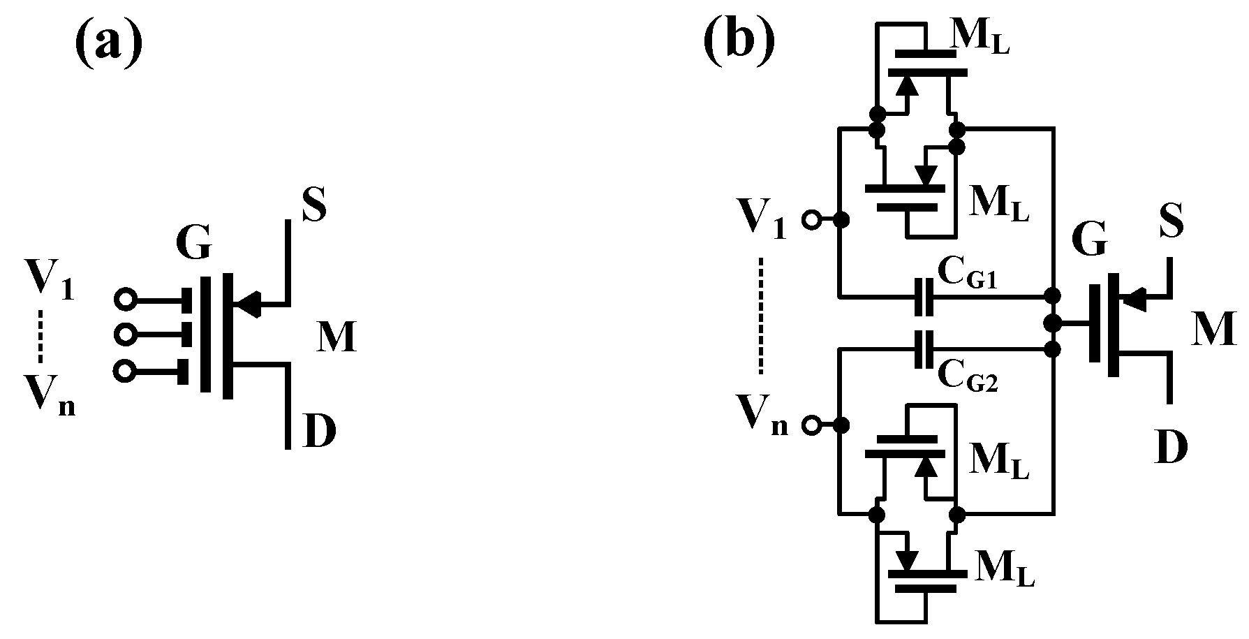
2.1. Proposed MI-DDTA

Figure 1a shows the electrical symbol of the MI-DDTA. The low-frequency characteristics of the device are given by:
V w = V y + 1 + V y + 2 V y 1 V y 2 I o = g m V w
In brief, the operation of the circuit could be characterized as follows: the voltage at the low-impedance output w is a sum of two differential input voltages V y 1 = V y + 1 V y 2 and V y 2 = V y + 2 V y 1 . The output current I o at the high-impedance output o is equal to the product of V w , and a transconductance gain g m , namely, the second equation of (1) describes a voltage-controlled current source. The CMOS structure of the proposed MI-DDTA is shown in Figure 1b. It consists of a differential difference amplifier (DDA) with unity gain feedback, followed by a transconductance amplifier (TA).
The unity gain DDA consists of a differential stage based on the flipped voltage follower M1-M5 that allowed the minimum voltage supply to be as low as the sum of one gate-source (VGS-M3) and one drain source (VDS-M5) voltage, i.e., VDDmin = VGS-M3 + VDS-M5; hence, the low voltage supply capability is guaranteed. To increase the number of inputs of the differential pair M1 and M2, the multiple-input gate-driven MOS transistor (MI-GD-MOST) technique is used [31,32,33,34,35,36]. This multiple-input increase the arithmetic operation capability of the DDTA circuit.
The symbol of the MI-GD-MOST and its implementation is shown in Figure 2. The arbitrary number of inputs V1, … Vn are simply obtained by parallel connection of the input capacitor CG and two anti-parallel MOS transistors ML operating in cutoff region, hence creating high resistance value with minimum occupied chip area. These high resistances are essential for proper DC operation of the circuit while the input capacitors ensure the AC path for the input signals. The second stage of the unity gain DDA is created by class-AB stage M6, M7 and high resistance RMOS. This RMOS is also created by two cut-off transistors ML, and ensures the proper DC bias current of this output stage, while the capacitor C ensures the AC path for the signal; hence a simple class-AB stage is obtained. The compensation capacitor Cc ensure the stability of the DDA circuit.
β = α · g m 1 , 2 r d s 1 , 2 | | r d s 4 , 5 g m 6 + g m 7 r d s 1 , 2 | | r d s 4 , 5 1 + α · g m 1 , 2 r d s 1 , 2 | | r d s 4 , 5 g m 6 + g m 7 r d s 1 , 2 | | r d s 4 , 5
where β is the voltage gain of the capacitive voltage divider, at the gates of M1 and M2, which neglecting the impact of the parasitic capacitances of MOS transistor, can be approximated as:
α C G 1 i = 0 n C G i
where n is the number of differential inputs of the MI- DDTA (note that one more capacitor CG0 is used in feedback connection). Assuming n = 2 and CG0 = CG1 = CG2 results in α = 1/3. The output resistance seen at the w terminal, Rw, is given by:
R w 1 α · g m 1 , 2 r d s 1 , 2 | | r d s 4 , 5 g m 6 + g m 7
Note, that both the low-frequency gain β, as well as the output resistance Rw, are deteriorated by the input capacitive divider. However, thanks to the two-stage architecture of the internal OTA, used to create the MI-DDTA, and class AB operation, both parameters can achieve acceptable values.
The input capacitance seen from a single y terminal, for identical capacitances CG, which are much larger than parasitic capacitances of an MOS transistor, is:
C y 2 3 C G
The gain bandwidth product (GBW) of the internal OTA, M1–M7, which is approximately equal to the 3-dB frequency of the gain β, depends on the transconductance of the input differential stage and the compensation capacitor CC:
G B W = α · g m 1 , 2 C c
The transconductance stage is realized using the mirror topology M8–M16. The structure employs the self-cascode connections M10c–M16c in order to increase the output resistance and the gain of the TA. The current ISET can be used to regulate the transconductance of the TA, which in the weak inversion region, with unity-gain current mirrors, is given by:
g m = I S E T n p U T
where np is the subthreshold slope factor for a p-channel MOS transistor and UT is the thermal potential.
The output resistance of the TA, i.e., the resistance seen from its o output, Ro, can be approximated as:
R o ( g m 10 r d s 10 r d s 10 c ) | | ( g m 15 r d s 15 r d s 15 c )
and its DC voltage gain ATA is given by:
A T A = g m R o
The parasitic poles associated with internal nodes of the TA are located well above the GBW product of the TA, consequently, the GBW product depends on the loading capacitance at the o terminal CLTA, and is given by:
G B W T A = g m C L T A

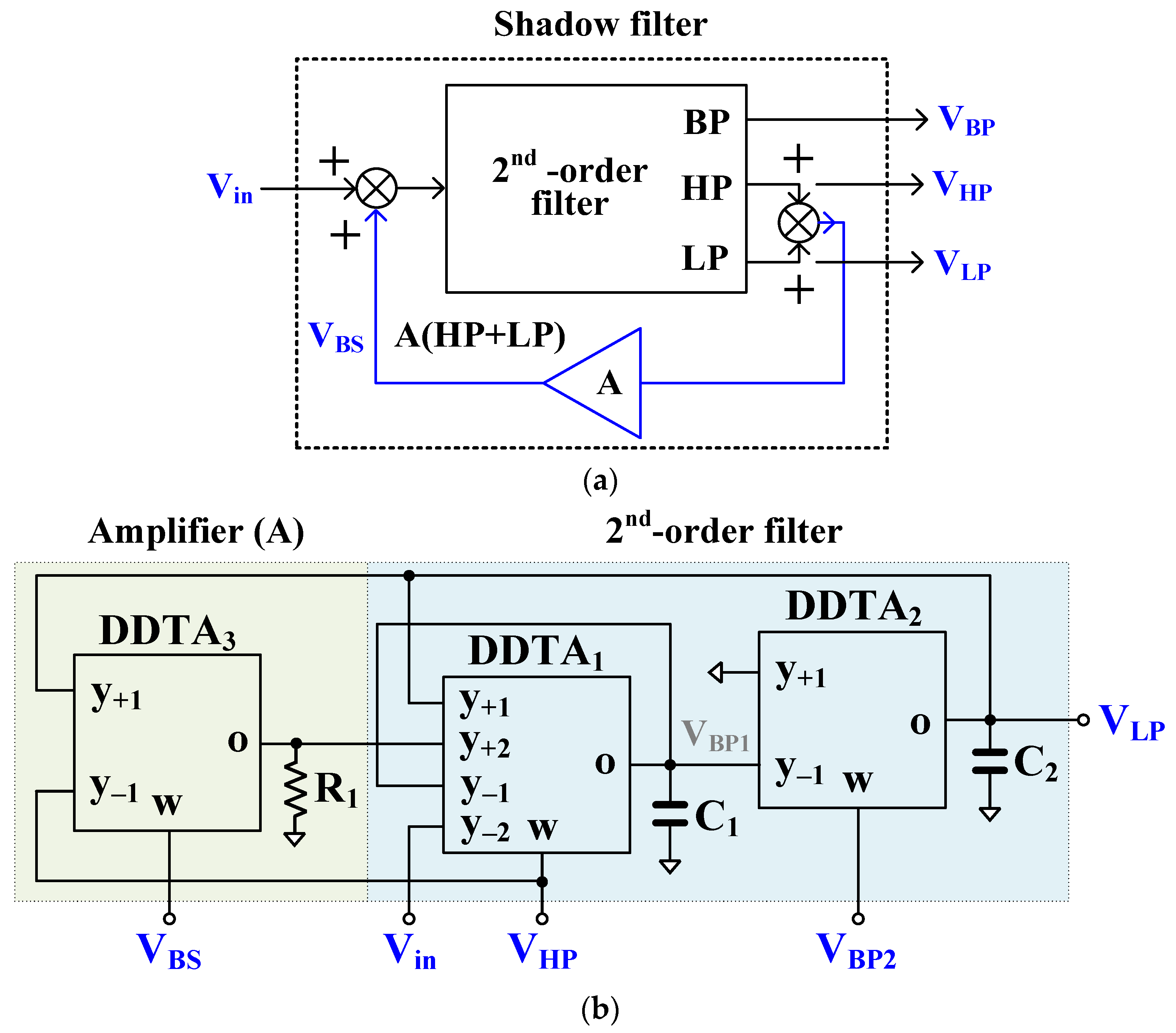
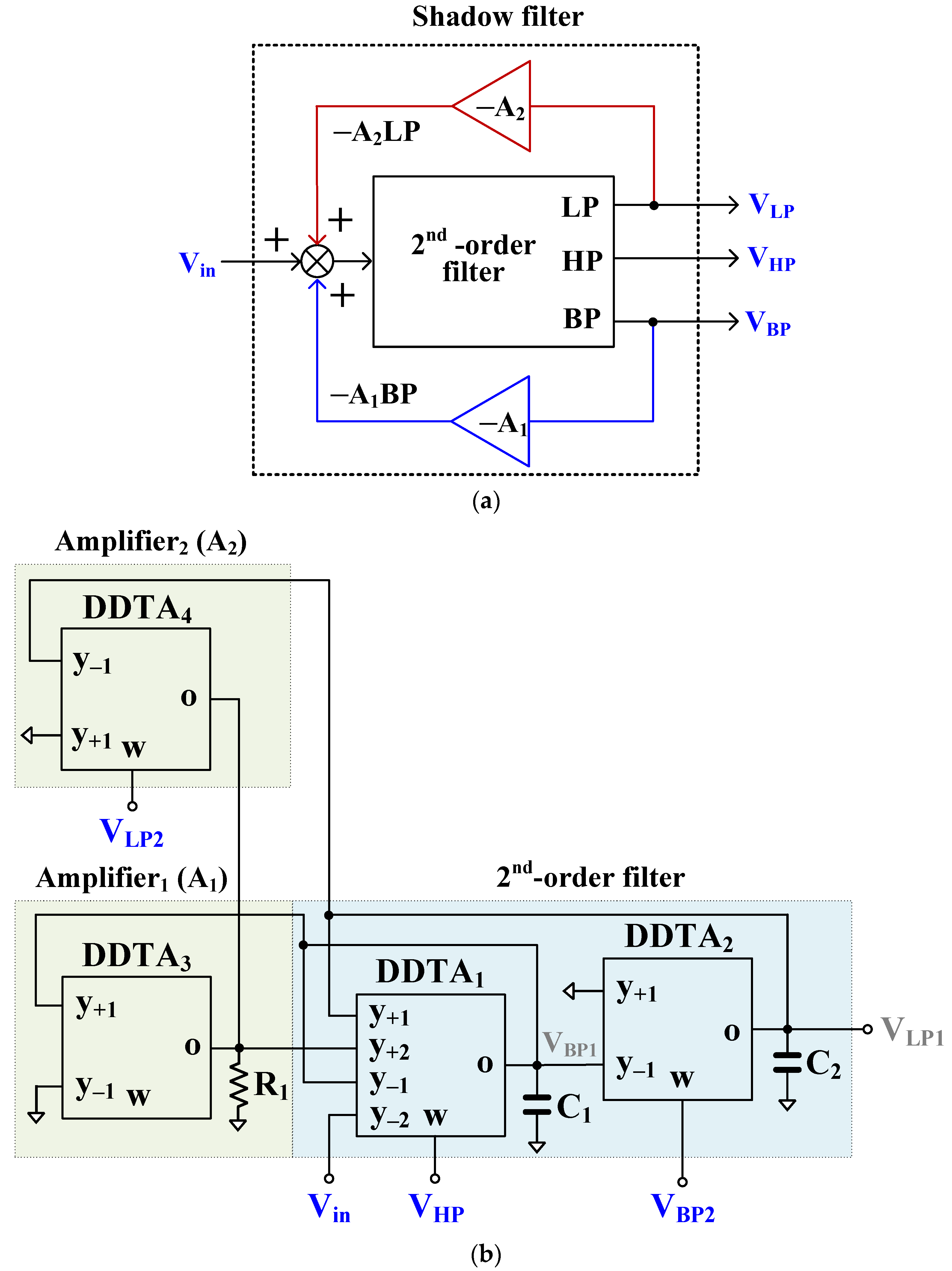
2.2. Proposed Shadow Filters

Figure 3a shows the block diagram of the shadow filter [10] that has been used to realize the first proposed shadow filter as shown in Figure 3b. The DDTA1, DDTA2 along with capacitors C1 and C2 realize the 2nd-order filter while DDTA3 along with resistor R1 realize the amplifier (A). The inverting high-pass (HP) and band-pass (BP) responses are obtained at the VHP and VBP1 outputs, respectively, while VLP, VBP2, and VBS provide non-inverting low-pass (LP), BP, and band-stop (BS) responses. It should be noted that the input Vin possesses high impedance and outputs VHP, VBP2, and VBS possess low impedance while the output VLP needs the buffer circuit if low-impedance load is connected. The outputs VLP and VHP are summed and amplified. Using (1) and nodal analysis, the transfer functions of LP, HP, BP and BS filters can be expressed by:
V L P V i n = g m 1 g m 2 1 1 + g m 3 R 1 s 2 C 1 C 2 + s C 2 g m 1 1 1 + g m 3 R 1 + g m 1 g m 2
V H P V i n = s 2 C 1 C 2 1 1 + g m 3 R 1 s 2 C 1 C 2 + s C 2 g m 1 1 1 + g m 3 R 1 + g m 1 g m 2
V B P 2 V i n = V B P 1 V i n = s C 2 g m 1 1 1 + g m 3 R 1 s 2 C 1 C 2 + s C 2 g m 1 1 1 + g m 3 R 1 + g m 1 g m 2
V B S V i n = s 2 C 1 C 2 1 1 + g m 3 R 1 + g m 1 g m 2 1 1 + g m 3 R 1 s 2 C 1 C 2 + s C 2 g m 1 1 1 + g m 3 R 1 + g m 1 g m 2
where g m 3 R 1 = A . The gain A can be regulated by g m 3 , with constant R 1 , or by regulating R 1 with constant g m 3 .
The natural frequency ( ω o ) and the quality factor ( Q ) are given by:
ω o = g m 1 g m 2 C 1 C 2
Q = 1 + A g m 2 C 1 g m 1 C 2
From (15), the parameter ω o can be controlled by g m 1   =   g m 2 and from (16), the parameter Q can be controlled by A (i.e., regulating gm3 with constant R 1 ) while maintaining g m 1 = g m 2 and C 1 = C 2 . Thus, the parameters ω o and Q can be controlled electronically.
From (11)–(14), increasing the parameter Q will decrease the passband of LP and HP filters by 1 / 1 + A , whereas the gain of the BP filter will be constant.
It should be noted from (16) that the parameter Q can be increased if A > 1 . When the amplifier inputs are swapped (i.e., connecting the y−1-terminal to VLP and the y+1-terminal to VHP), the parameter Q will be proportional to 1 A . In this case 0 < A < 1 is used.
The block diagram of the second proposed shadow filter is shown in Figure 4a. In this system two amplifiers A1 and A2 are used to amplify the output signals VBP and VLP, respectively. The proposed filter, employing four MI-DDTAs, two grounded capacitors, and one resistor is shown in Figure 4b. The DDTA1 and DDTA2, along with capacitors C1 and C2 are used to realize the 2nd order filter while the resistor R1 along with the DDTA1 and DDTA2, respectively, are used to realize the amplifiers A1 and A2. The non-inverting LP and BP responses are obtained at the VLP1 and VBP2 outputs, respectively, while VLP2, VHP, and VBP1 provide inverting LP, HP, and BP responses. It should be noted that the input Vin possesses high impedance while the outputs VLP2, VHP, and VBP2 possess low impedance. The output VBP1 is amplified by A1 using DDTA3 and resistor R1 and the output VLP1 is amplified by A2 using DDTA4 and the same resistor R1.
Using (1) and nodal analysis, the transfer function of the second proposed filter in Figure 4b can be expressed by:
V L P 1 V i n = V L P 2 V i n = g m 1 g m 2 s 2 C 1 C 2 + s C 2 g m 1 1 g m 3 R 1 + g m 1 g m 2 1 g m 4 R 1
V H P V i n = s 2 C 1 C 2 s 2 C 1 C 2 + s C 2 g m 1 1 g m 3 R 1 + g m 1 g m 2 1 g m 4 R 1
V B P 2 V i n = V B P 1 V i n = s C 2 g m 1 s 2 C 1 C 2 + s C 2 g m 1 1 g m 3 R 1 + g m 1 g m 2 1 g m 4 R 1
where g m 3 R 1 = A 1 and g m 4 R 1 = A 2 . From (17)–(19), they are valid for A 1 < 1 and A 2 < 1 . The natural frequency of the filter and its quality factor can be expressed as:
ω o = 1 A 2 g m 1 g m 2 C 1 C 2
= 1 A 2 1 A 1 g m 2 C 1 g m 1 C 2
From (20), the parameter ω o can be controlled by A 2 through adjusting g m 4 or by adjusting g m 1 = g m 2 . However, adjusting the parameter ω o by A 2 affects the parameter Q . The parameter Q can be controlled by A 1 without affecting the parameter ω o through adjusting g m 3 . From (17)–(20), adjusting the parameter ω o will change the passband of LP and BP filters whereas the passband of HP filter is constant.

2.3. Non-Idealities Analysis

The non-idealities of DDTA can be considered as
V w = β + j 1 V y + 1 + β + j 2 V y + 2 β j 1 V y 1 β j 2 V y 2 I o = g m n j V w
where β + j 1 = 1 ε + j 1 v and ε + j 1 v ( ε + j 1 v 1 ) denote the voltage tracking error from V y + 1 to V w of the j -th DDTA, β + j 2 = 1 ε + j 2 v and ε + j 2 v ( ε + j 2 v 1 ) denote the voltage tracking error from V y + 2 to V w of the j -th DDTA,   β j 1 = 1 ε j 1 v and ε j 1 v   ( ε j 1 v 1 ) denote the voltage tracking error from V y 1 to V w of the j -th DDTA, and   β j 2 = 1 ε j 2 v and ε j 2 v   ( ε j 2 v 1 ) denote the voltage tracking error from V y 1 to V w of the j -th DDTA, and g m n j is the frequency-dependent transconductance that typically determined the operation frequency ω o [40]. The non-ideal of transconductance g m n j can be expressed as [41,42].
g m n j s g m j 1 μ j s
The non-ideal first transfer function of the proposed shadow filter in Figure 3a can be expressed by:
V L P V i n = g m n 1 g m n 2 β 22 β 32 1 1 + g m 3 R 1 β 11 β + 22 s 2 C 1 C 2 + s C 2 g m n 1 β 21 1 1 + g m 3 R 1 β 11 β + 22 + g m n 1 g m n 2 β 31 β + 21 + g m 3 R 1 β + 11 β + 22 1 + g m 3 R 1 β 11 β + 22
V H P V i n = s 2 C 1 C 2 β 22 1 1 + g m 3 R 1 β 11 β + 22 s 2 C 1 C 2 + s C 2 g m n 1 β 21 1 1 + g m 3 R 1 β 11 β + 22 + g m n 1 g m n 2 β 31 β + 21 + g m 3 R 1 β + 11 β + 22 1 + g m 3 R 1 β 11 β + 22
V B P 2 V i n = V B P 1 V i n = s C 2 g m n 1 β 22 1 1 + g m 3 R 1 β 11 β + 22 s 2 C 1 C 2 + s C 2 g m n 1 β 21 1 1 + g m 3 R 1 β 11 β + 22 + g m n 1 g m n 2 β 31 β + 21 + g m 3 R 1 β + 11 β + 22 1 + g m 3 R 1 β 11 β + 22
where g m n 3 R 1 = A
ω o = g m n 1 g m n 2 β 31 C 1 C 2 β 21 + + g m n 3 R 1 β + 11 β 22 + 1 + g m n 3 R 1 β 11 β 22 +
Using (23), D s of the transfer functions can be rewritten as:
Q = 1 + g m n 3 R 1 β 11 β + 22 β 21 C 1 g m n 2 β 31 C 2 g m n 1 β 21 + + g m n 3 R 1 β + 11 β 22 + 1 + g m n 3 R 1 β 11 β 22 +
where:
s 2 C 1 C 2 1 C 2 g m 1 μ 1 β 21 B g m 1 g m 2 μ 1 μ 2 β 31 C C 1 C 2 + s C 2 g m 1 β 21 B ( 1 g m 1 g m 2 β 31 μ 1 + g m 1 g m 2 β 31 μ 2 C C 2 g m 1 β 21 B ) + g m 1 g m 2 β 31 C
where:
B = 1 1 + g m 3 R 1 β 11 β + 22 ,   C = β + 21 + g m 3 R 1 β + 11 β + 22 1 + g m 3 R 1 β 11 β + 22
The non-ideality of transconductance   g m n can be neglected by satisfying the following condition:
C 2 g m 1 μ 1 β 21 B g m 1 g m 2 μ 1 μ 2 β 31 C C 1 C 2 1
g m 1 g m 2 β 31 μ 1 + g m 1 g m 2 β 31 μ 2 C C 2 g m 1 β 21 B 1
The non-ideal transfer function of the second proposed shadow filter in Figure 4b can be expressed by
V L P 1 V i n = V L P 2 V i n = g m n 1 g m n 2 β 21 β 22 s 2 C 1 C 2 + s C 2 g m n 1 β 21 g m n 3 R 1 β + 31 β + 22 + g m n 1 g m n 2 β 21 β + 21 g m n 4 R 1 β 41 β + 22
V H P V i n = s 2 C 1 C 2 β 22 s 2 C 1 C 2 + s C 2 g m n 1 β 21 g m n 3 R 1 β + 31 β + 22 + g m n 1 g m n 2 β 21 β + 21 g m n 4 R 1 β 41 β + 22
V B P 2 V i n = V B P 1 V i n = s C 2 g m n 1 β 22 s 2 C 1 C 2 + s C 2 g m n 1 β 21 g m n 3 R 1 β + 31 β + 22 + g m n 1 g m n 2 β 21 β + 21 g m n 4 R 1 β 41 β + 22
where g m n 3 R 1 = A 1 and g m n 4 R 1 = A 2
ω o = β + 21 g m n 4 R 1 β 41 β + 22 g m n 1 g m n 2 β 21 C 1 C 2
Q = β + 21 g m n 4 R 1 β 41 β + 22 β 21 g m n 3 R 1 β 31 β + 22 C 1 g m n 2 β 21 C 2 g m n 1
Using (23), D s of the transfer functions can be rewritten as
s 2 C 1 C 2 1 C 2 g m 1 μ 1 D g m 1 g m 2 β 21 μ 1 μ 2 E C 1 C 2 + s C 2 g m 1 D 1 g m 1 g m 2 β 21 μ 1 E + g m 1 g m 2 β 21 μ 2 E C 2 g m 1 D + g m 1 g m 2 β 21 E
where D = β 21 g m n 3 R 1 β + 31 β + 22 , and E = β + 21 g m n 4 R 1 β 41 β + 22 . The non-ideality of the transconductance g m n can be neglected by satisfying the following condition:
C 2 g m 1 μ 1 D g m 1 g m 2 β 21 μ 1 μ 2 E C 1 C 2 1
g m 1 g m 2 β 21 μ 1 E + g m 1 g m 2 β 21 μ 2 E C 2 g m 1 D 1
Considering the parasitic parameters of DDTA by letting y-terminals possess very high impedance levels, which can be neglected, low parasitic resistance R w at w-terminal and parallel of parasitic capacitance C o and resistance R o at o-terminal. From Figure 3b and Figure 4b, the parasitic parameters C o 1 and R o 1 of DDTA1 are parallel with C 1 , parasitic parameters C o 2 and R o 2 of DDTA2 are parallel with C 2 , and parasitic parameters C o 3 and R o 3 of DDTA2 are parallel with R 1 . These parasitic parameters can be neglected by choosing appropriately values such as g m j 1 / R o j , C j C o j , and R 1 R o j , where j = 1 ,   2 ,   3 of DDTA j .

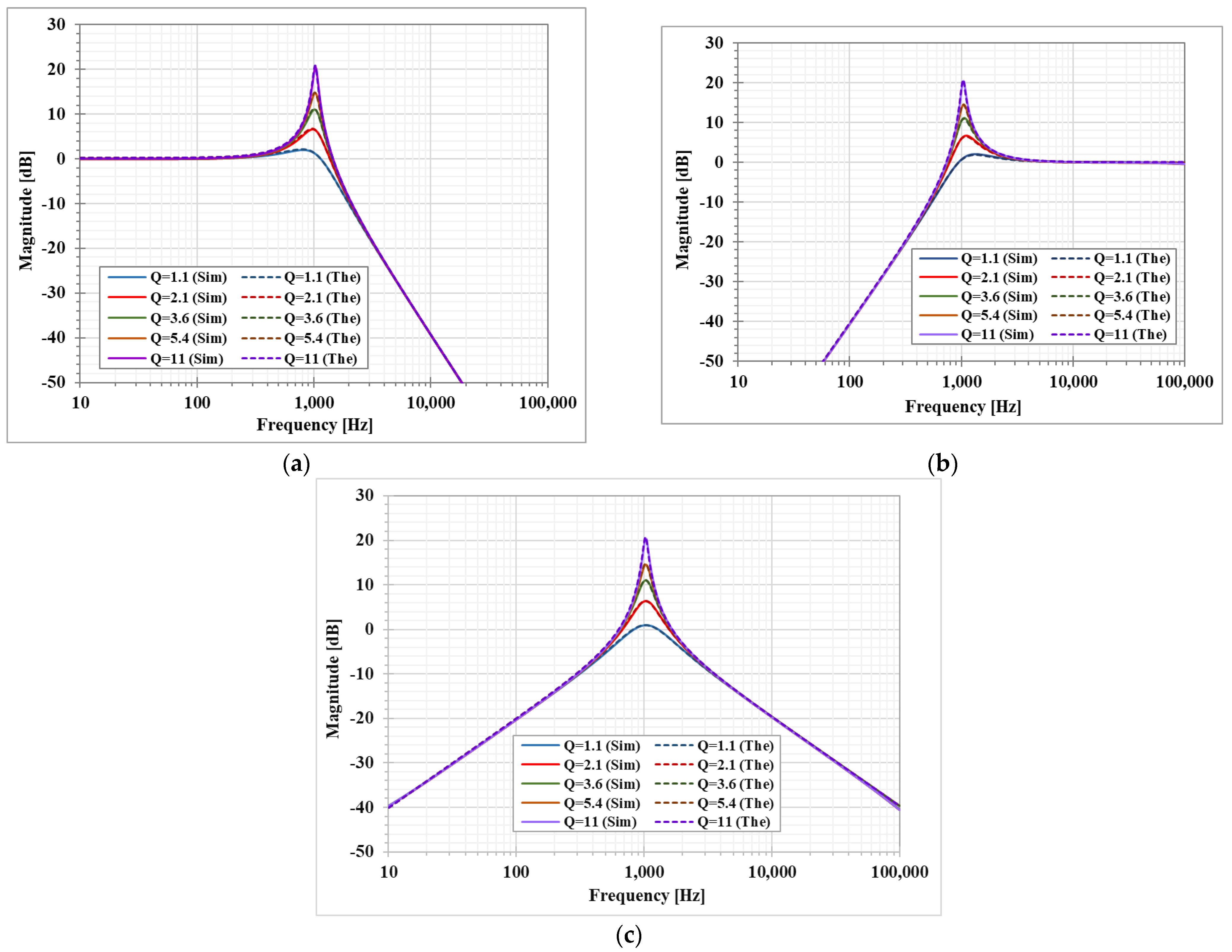
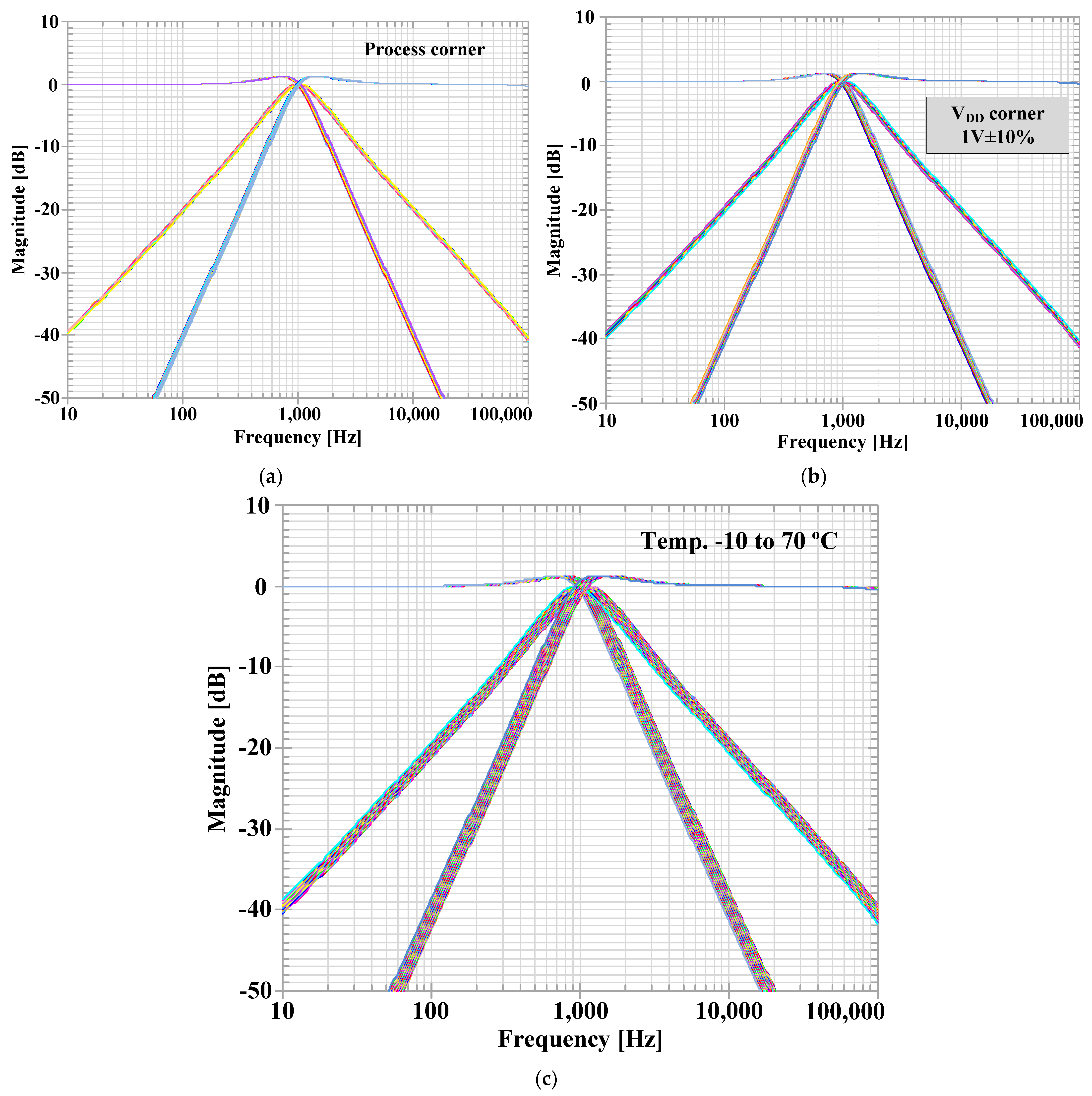
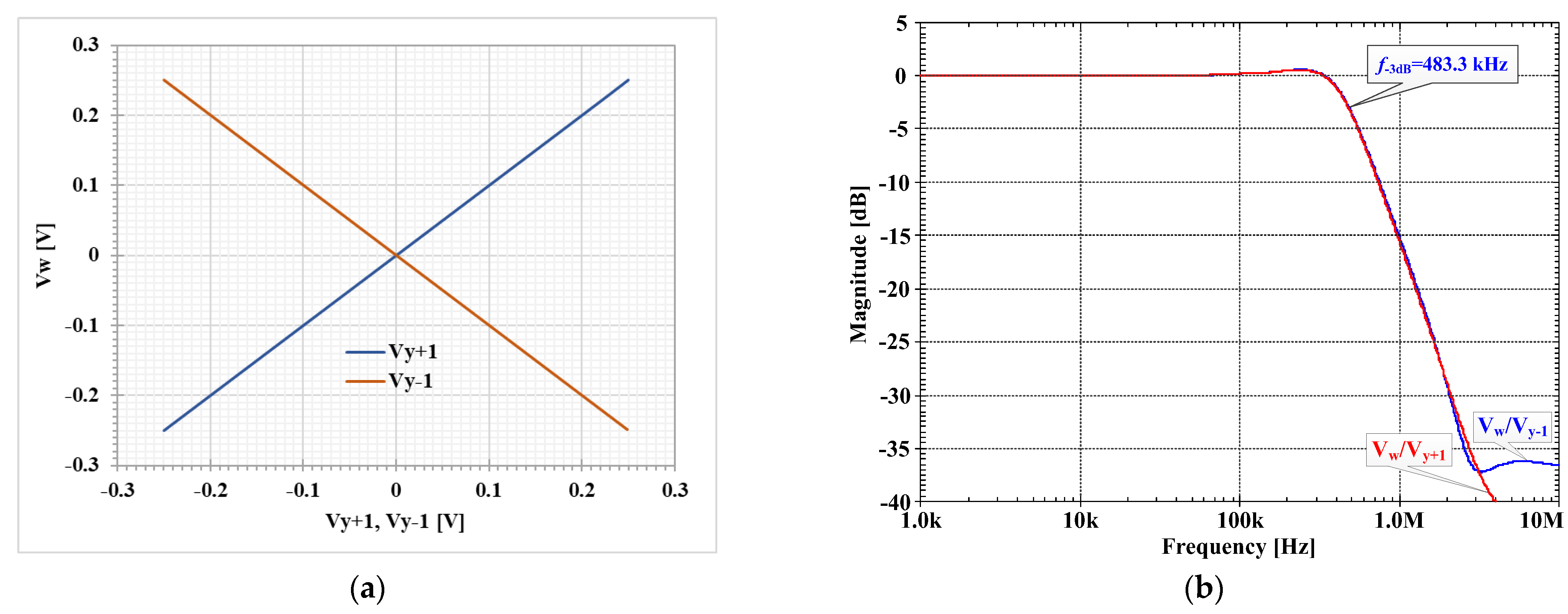
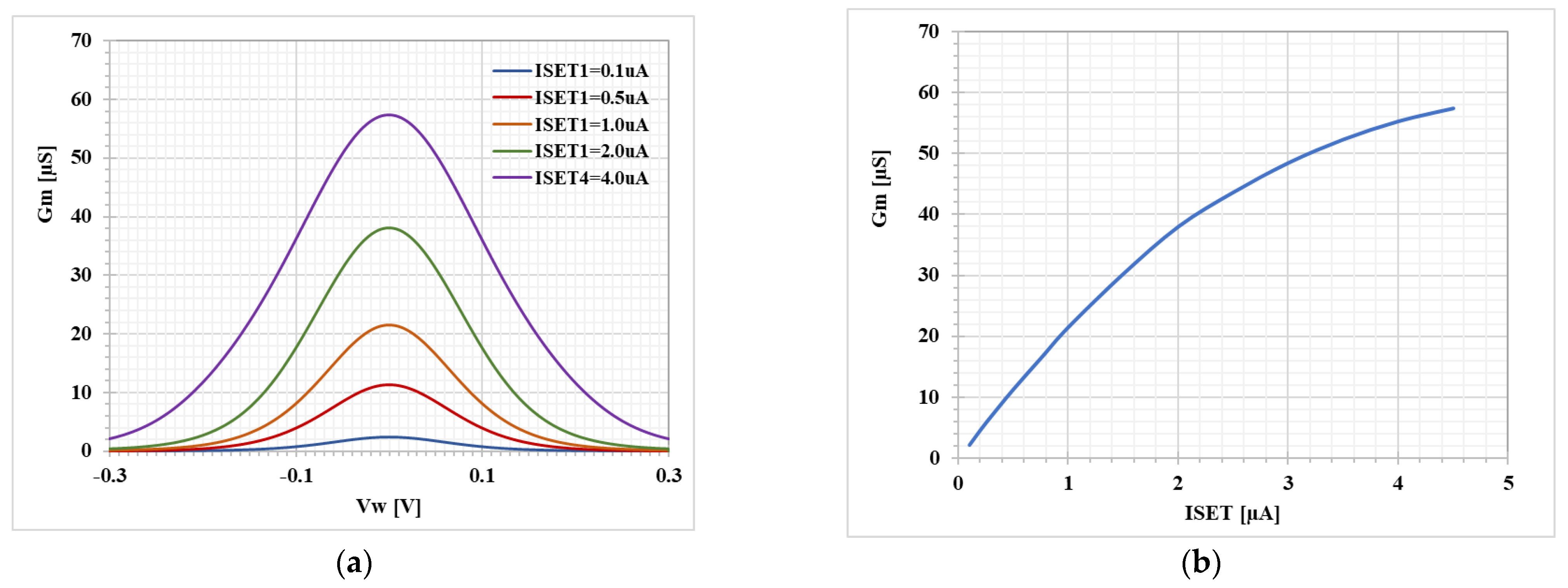
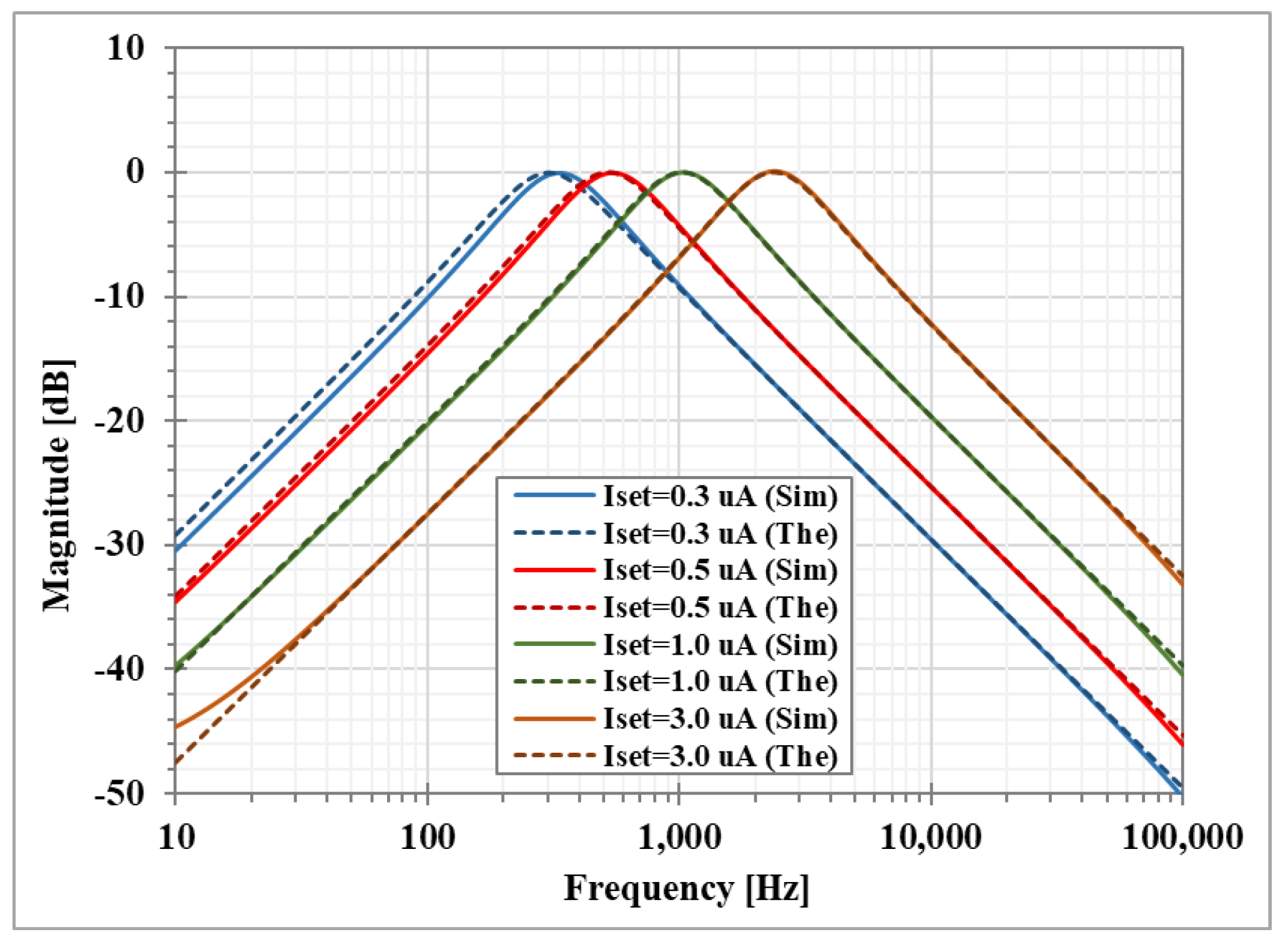
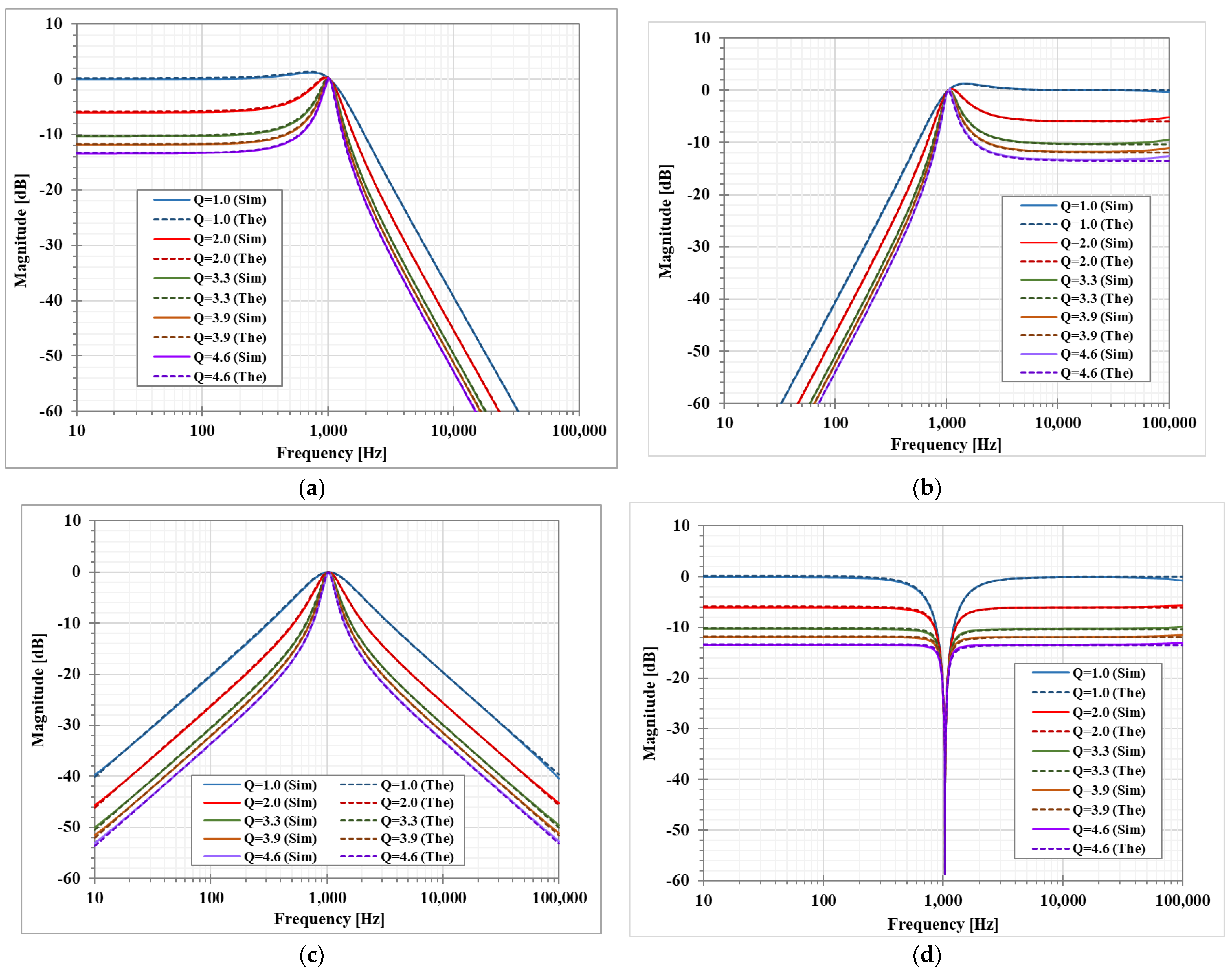
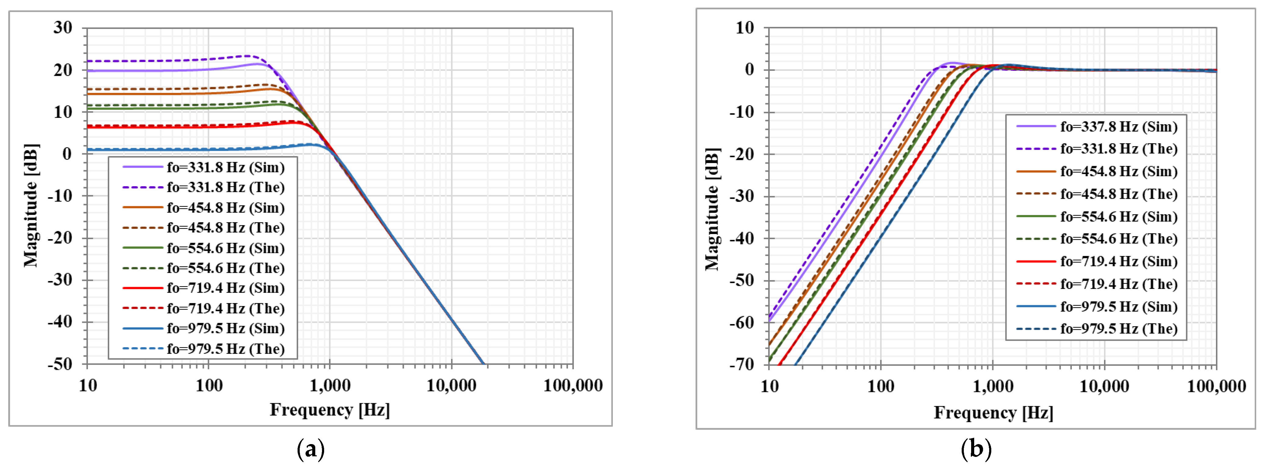
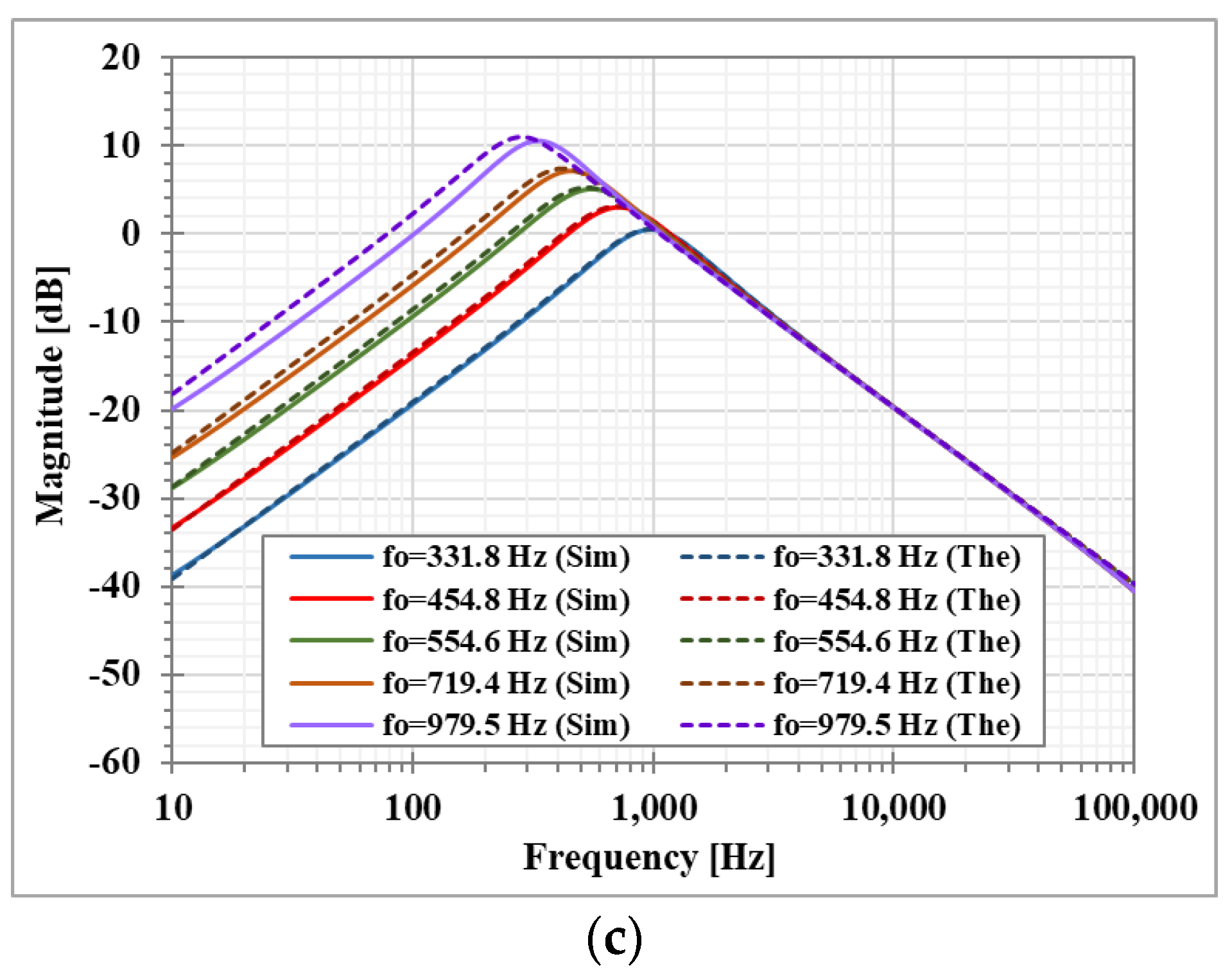
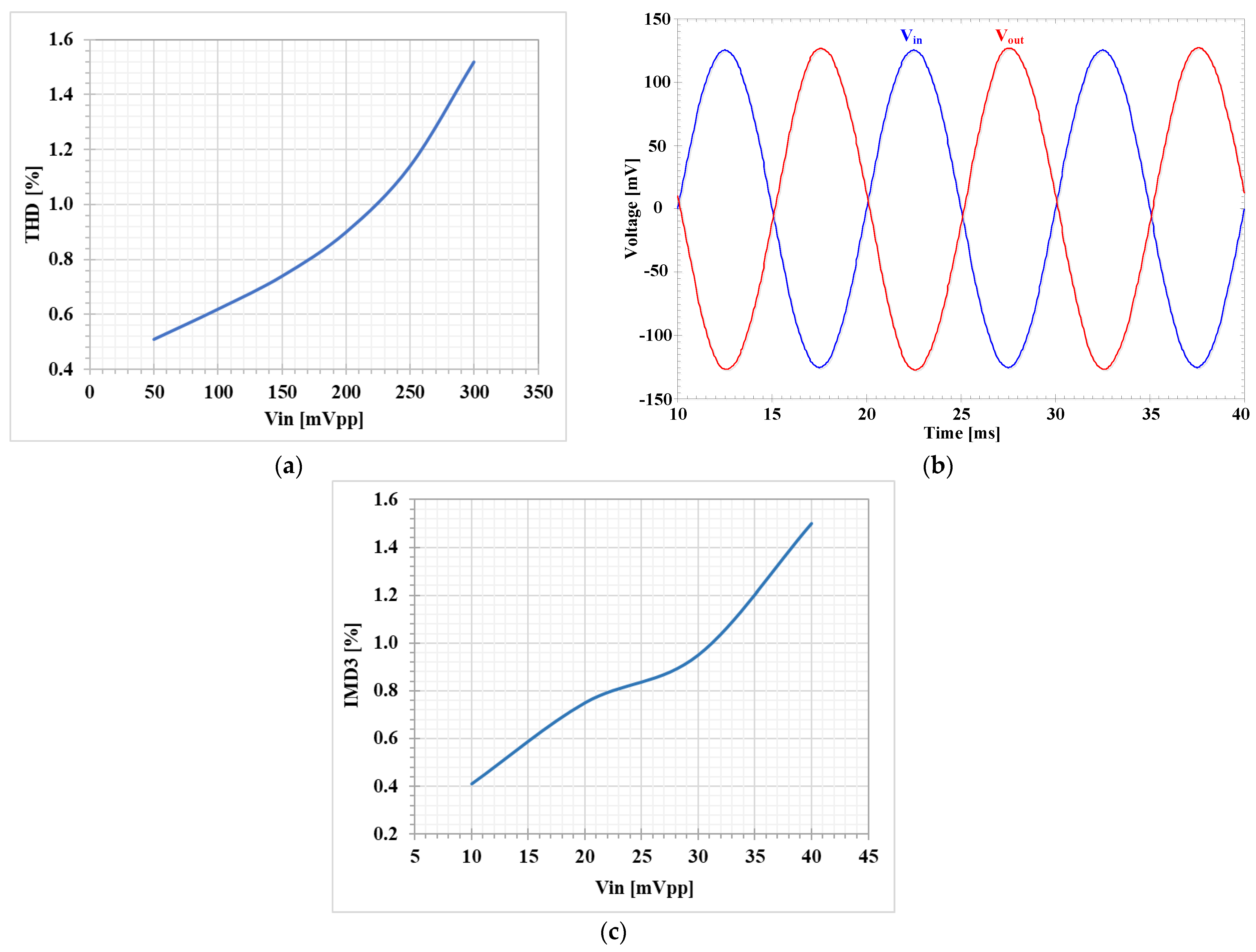
3. Simulation Results

The proposed shadow filters were simulated using SPICE. The MI-DDTA as shown in Figure 1a was designed using a 0.18 μm CMOS technology and the transistor aspect ratios are shown in Table 1. The power supply was ±0.5 V.
Figure 5a shows the DC transfer characteristic V w against V y + 1 and V y 1 of the MI-DDTA while (b) shows the AC transfer characteristic and −3 dB bandwidth of Vw/Vy+1 and Vw/Vy−1 with load capacitance of 10 pF, the −3 dB bandwidth is around 483.3 kHz and the low frequency gain is −0.016 dB. It is notable the capability of operation in a wide range of the input voltages. Note, that both, the differential, as well as common-mode range of the input differential amplifier M1–M2 is increased 1/α times, thanks to the input capacitive divider.
Figure 6 shows the small-signal transconductance of the transconductance stage, against the input voltage V w , for different I SET (Figure 6a), and against ISET (Figure 6b). It is worth noting that although the input range is sufficient for the proposed applications, this range, if needed, could be simply increased using a linearization technique like the source degeneration that results in increased dynamic rang of the system. The parasitic parameters of DDTA are Ry = 6.28 GΩ, R w = 540 Ω, R o = 11.9 MΩ, and C o = 33.67 fF.
The first proposed shadow filter was designed with C1 = C2 = 3.3 nF and R1 = 46.5 kΩ. Note that these passive values are sufficient to avoid the impact of parasitic effects. The transconductance g m 3 adjusted by the current ISET3 was used to control the amplifier A. The bias currents ISET1 and ISET2 were used to control g m 1 and g m 2 , respectively.
The first simulation was performed with A = 0, by setting the bias current ISET3 = 0 and ISET1 = ISET2 = 1 μA ( g m = 21.5 μS). This setting resulted in natural frequency (fo) of 1.036 kHz and the quality factor (Q) of 1.
The magnitude responses of the LP, HP, BP, and BS filters are shown in Figure 7. Figure 8 shows the magnitude responses of the BP filter when the bias currents ISET1 = ISET2 are varied. This result confirms that the natural frequency of the shadow filter can be electronically controlled. Figure 9 shows the magnitude frequency responses when the amplifier A is used to set the quality factor Q equal to 1.0, 2.0, 3.2, 3.9, and 4.6. Figure 9c shows that the quality factor of the BP filter can be controlled by the amplifier A ( A > 1) with the passband gain equal to 0 dB while the passband gain of the LP, HP and BS filters in Figure 9a–c respectively, will decrease when the quality factor is increased.
The second proposed shadow filter was designed with C1 = C2 = 3.3 nF and R1 = 46.5 kΩ. The bias currents ISET1 and ISET2 were used to adjust g m 1 and g m 2 , respectively. The g m 3 that was adjusted by ISET3 and g m 4 adjusted by ISET4 were used to control the amplifiers A 1 and A 2 , respectively. The first simulation was performed with A 2 = 0 by setting the bias currents ISET4= 0, ISET1 = ISET2 = 1 μA ( g m = 21.5 μS), while the amplifier A 1 was used to control the parameter Q. The simulated magnitude responses of the LP, HP, and BP filters with Q = 1.1, 2.1, 3.6, 4.5, 10.0 are shown in Figure 10. This result confirmed that the parameter Q can be controlled by A 1 , without affecting the parameter ω o .
Figure 11 shows the simulated magnitude frequency responses of the LP, HP, and BP filters when the amplifier A 2 gain was regulated by g m 4 and the amplifier A 1 was used to control the parameter Q = 1. This result confirmed that when the parameter ω o is varied by the amplifier A 2 , the passband gain of the LP and BP filter is changing while the passband gain of the HP filter is constant.
Figure 12a shows the simulated total harmonic distortion (THD) of the LP filter for f = 100 Hz. The amplifiers A1 and A2 were not active (ISET3 = ISET4 = 0 A). It can be noticed that THD was less than 1.2% for Vin < 250 mVpp and its transient response is shown in Figure 12b. Figure 12c shows the simulated third intermodulation distortion (IMD3) of the BP filter for a two-tone test, with two closely spaced tones of f1 = 0.9 kHz and f2 = 1.1 kHz. The IMD3 was less than 1.5% for the input amplitude up to 40 mVpp.
The simulated magnitude responses of the LP, HP, and BP filters for process, voltage, and temperature (PVT) corners were investigated. Figure 13a–c show respectively the results of Monte Carlo (MC) analysis, were variations of the threshold voltages of MOS transistors by 10% (LOT tolerance), supply voltages by +/− 10% and temperature from −10 °C to 70 °C were assumed. As it can be noticed, the proposed filter is robust under the assumed PVT variations.
Finally, Table 2 provides a comparison of the proposed filters with previously published shadow filters in [22,23,26,29,30]. The proposed filters provide lower power consumption, as compared with [22,23], lower output impedance, as compared with [26,30] (except the output impedance of the LP filter in Figure 3b), larger number of low-impedance nodes, as compared with [29], and lower supply voltage, as compared with [23,26,29,30].

4. Conclusions

This paper presents new voltage-mode shadow filters with single-input multiple-output topology, using low-voltage low-power multiple-input differential difference transconductance amplifiers. The multiple-input DDTA can be easily realized using MIGD-MOST technique. The proposed filters offer high-input impedance and most of the output terminals offer low-impedance. The natural frequency and the quality factor of the filters can be electronically and independently controlled. The impact of the non-idealities of the DDTA on the performance of the proposed shadow filter is studied. The SPICE simulation results using 0.18 μm CMOS process from TSMC is given to validate the workability of the new circuits.

Author Contributions

Conceptualization, M.K., F.K. and T.K.; methodology, M.K. and F.K.; software, M.K. and F.K.; validation, F.K. and T.K.; formal analysis, T.K., M.K. and F.K., investigation, F.K. and M.K.; resources, F.K. and M.K.; writing—original draft preparation, F.K., T.K. and M.K.; writing—review and editing, F.K. and T.K.; visualization, F.K., T.K. and M.K.; supervision, F.K.; project administration, F.K.; funding acquisition, F.K. All authors have read and agreed to the published version of the manuscript.

Funding

This work was supported by the University of Defence within the Organization Development Project VAROPS.

Conflicts of Interest

The authors declare no conflict of interest.

References

  1. Unuk, T.; Yuce, E. Supplementary DDCC+ based universal filter with grounded passive elements. AEU-Int. J. Electron. Commun. 2021, 132, 153652. [Google Scholar] [CrossRef]
  2. Shankar, C.; Singh, S.V.; Imam, R. SIFO–VM/TIM universal biquad filter using single DVCCTA with fully CMOS realization. Analog. Integr. Circuits Signal Process. 2021, 109, 33–46. [Google Scholar] [CrossRef]
  3. Roongmuanpha, N.; Faseehuddin, M.; Herencsar, N.; Tangsrirat, W. Tunable Mixed-Mode Voltage Differencing Buffered Amplifier-Based Universal Filter with Independently High-Q Factor Controllability. Appl. Sci. 2021, 11, 9606. [Google Scholar] [CrossRef]
  4. Mishra, R.; Mishra, G.R.; Mishra, S.O.; Faseehuddin, M. Electronically Tunable Mixed Mode Universal Filter Employing Grounded Passive Components. Inf. MIDEM-J. Microelectron. Electron. Components Mater. 2022, 52, 105–115. [Google Scholar] [CrossRef]
  5. Bhaskar, D.; Raj, A.; Senani, R. Three new CFOA-based SIMO-type universal active filter configurations with unrivalled features. AEU-Int. J. Electron. Commun. 2022, 153, 154285. [Google Scholar] [CrossRef]
  6. Alexander, C.K.; Sadiku, M. Fundamental of Electric Circuits; McGraw-Hill: New York, NY, USA, 2004. [Google Scholar]
  7. Best, R. Phase Locked Loops: Design, Simulation, and Applications, 6th ed.; McGraw Hill: New York, NY, USA, 2007. [Google Scholar]
  8. Schaumann, R.; Ghausi, M.; Laker, K. Design of Analog Filter: Passive, Active RC, and Switched Capacitor; Prentice Hall: New York, NY, USA, 1990. [Google Scholar]
  9. Lakys, Y.; Fabre, A. Shadow filters—New family of second-order filters. Electron. Lett. 2010, 46, 276–277. [Google Scholar] [CrossRef]
  10. Biolkova, V.; Biolek, D. Shadow filters for orthogonal modification of characteristic frequency and bandwidth. Electron. Lett. 2010, 46, 830–831. [Google Scholar] [CrossRef]
  11. Pandey, N.; Pandey, R.; Choudhary, R.; Sayal, A.; Tripathi, M. Realization of CDTA based frequency agile filter. In Proceedings of the 2013 IEEE International Conference on Signal Processing, Computing and Control (ISPCC), Solan, India, 26–28 September 2013; pp. 1–6. [Google Scholar] [CrossRef]
  12. Alaybeyoğlu, E.; Guney, A.; Altun, M.; Kuntman, H. Design of positive feedback driven current-mode amplifiers Z-Copy CDBA and CDTA, and filter applications. Analog. Integr. Circuits Signal Process. 2014, 81, 109–120. [Google Scholar] [CrossRef]
  13. Atasoyu, M.; Kuntman, H.; Metin, B.; Herencsar, N.; Cicekoglu, O. Design of current-mode class 1 frequency-agile filter employing CDTAs. In Proceedings of the 2015 European Conference on Circuit Theory and Design (ECCTD), Trondheim, Norway, 24–26 August 2015; pp. 1–4. [Google Scholar] [CrossRef]
  14. Alaybeyoğlu, E.; Kuntman, H. A new frequency agile filter structure employing CDTA for positioning systems and secure communications. Analog. Integr. Circuits Signal Process. 2016, 89, 693–703. [Google Scholar] [CrossRef]
  15. Nand, D.; Pandey, N. New Configuration for OFCC-Based CM SIMO Filter and its Application as Shadow Filter. Arab. J. Sci. Eng. 2018, 43, 3011–3022. [Google Scholar] [CrossRef]
  16. Chhabra, K.; Singhal, S.; Pandey, N. Realisation of CBTA Based Current Mode Frequency Agile Filter. In Proceedings of the 2019 6th International Conference on Signal Processing and Integrated Networks (SPIN), Noida, India, 7–8 March 2019; pp. 1076–1081. [Google Scholar] [CrossRef]
  17. Singh, D.; Paul, S.K. Realization of current mode universal shadow filter. AEU-Int. J. Electron. Commun. 2020, 117, 153088. [Google Scholar] [CrossRef]
  18. Singh, D.; Paul, S.K. Improved Current Mode Biquadratic Shadow Universal Filte. Inf. MIDEM-J. Microelectron. Electron. Components Mater. 2022, 51, 51–66. [Google Scholar] [CrossRef]
  19. Anurag, R.; Pandey, R.; Pandey, N.; Singh, M.; Jain, M. OTRA based shadow filters. In Proceedings of the 2015 Annual IEEE India Conference (INDICON), New Delhi, India, 17–20 December 2015; pp. 1–4. [Google Scholar] [CrossRef]
  20. Abuelma′Atti, M.T.; Almutairi, N. New voltage-mode bandpass shadow filter. In Proceedings of the 2016 13th International Multi-Conference on Systems, Signals & Devices (SSD), Leipzig, Germany, 21–24 March 2016; pp. 412–415. [Google Scholar] [CrossRef]
  21. Abuelma′Atti, M.T.; Almutairi, N. New CFOA-based shadow banpass filter. In Proceedings of the 2016 International Conference on Electronics, Information, and Communications (ICEIC), Danang, Vietnam, 27–30 January 2016; pp. 1–3. [Google Scholar] [CrossRef]
  22. Khateb, F.; Jaikla, W.; Kulej, T.; Kumngern, M.; Kubánek, D. Shadow filters based on DDCC. IET Circuits Devices Syst. 2017, 11, 631–637. [Google Scholar] [CrossRef]
  23. Alaybeyoğlu, E.; Kuntman, H. CMOS implementations of VDTA based frequency agile filters for encrypted communications. Analog. Integr. Circuits Signal Process. 2016, 89, 675–684. [Google Scholar] [CrossRef]
  24. Buakaew, S.; Narksarp, W.; Wongtaychatham, C. Fully Active and Minimal Shadow Bandpass Filter. In Proceedings of the 2018 International Conference on Engineering, Applied Sciences, and Technology (ICEAST), Phuket, Thailand, 4–7 July 2018; pp. 1–4. [Google Scholar] [CrossRef]
  25. Buakaew, S.; Narksarp, W.; Wongtaychatham, C. Shadow Bandpass Filter with Q-improvement. In Proceedings of the 2019 5th International Conference on Engineering, Applied Sciences and Technology (ICEAST), Luang Prabang, Laos, 2–5 July 2019; pp. 1–4. [Google Scholar] [CrossRef]
  26. Buakaew, S.; Narksarp, W.; Wongtaychatham, C. High Quality-Factor Shadow Bandpass Filters with Orthogonality to the Characteristic Frequency. In Proceedings of the 2020 17th International Conference on Electrical Engineering/Electronics, Computer, Telecommunications and Information Technology (ECTI-CON), Phuket, Thailand, 24–27 June 2020; pp. 372–375. [Google Scholar] [CrossRef]
  27. Moonmuang, P.; Pukkalanun, T.; Tangsrirat, W. Voltage Differencing Gain Amplifier-Based Shadow Filter: A Comparison Study. In Proceedings of the 2020 6th International Conference on Engineering, Applied Sciences and Technology (ICEAST), Chiang Mai, Thailand, 1–4 July 2020; pp. 1–4. [Google Scholar] [CrossRef]
  28. Buakaew, S.; Wongtaychatham, C. Boosting the Quality Factor of the Shadow Bandpass Filter. J. Circuits Syst. Comput. 2022, 31, 2250248. [Google Scholar] [CrossRef]
  29. Huaihongthong, P.; Chaichana, A.; Suwanjan, P.; Siripongdee, S.; Sunthonkanokpong, W.; Supavarasuwat, P.; Jaikla, W.; Khateb, F. Single-input multiple-output voltage-mode shadow filter based on VDDDAs. AEU-Int. J. Electron. Commun. 2019, 103, 13–23. [Google Scholar] [CrossRef]
  30. Varshney, G.; Pandey, N.; Pandey, R. Generalization of shadow filters in fractional domain. Int. J. Circuit Theory Appl. 2021, 49, 3248–3265. [Google Scholar] [CrossRef]
  31. Khateb, F.; Kulej, T.; Akbari, M.; Tang, K.-T. A 0.5-V Multiple-Input Bulk-Driven OTA in 0.18-μm CMOS. IEEE Trans. Very Large Scale Integr. (VLSI) Syst. 2022, 30, 1739–1747. [Google Scholar] [CrossRef]
  32. Kumngern, M.; Suksaibul, P.; Khateb, F.; Kulej, T. 1.2 V Differential Difference Transconductance Amplifier and Its Application in Mixed-Mode Universal Filter. Sensors 2022, 22, 3535. [Google Scholar] [CrossRef]
  33. Jaikla, W.; Bunrueangsak, S.; Khateb, F.; Kulej, T.; Suwanjan, P.; Supavarasuwat, P. Inductance Simulators and Their Application to the 4th Order Elliptic Lowpass Ladder Filter Using CMOS VD-DIBAs. Electronics 2021, 10, 684. [Google Scholar] [CrossRef]
  34. Kumngern, M.; Khateb, F.; Kulej, T.; Psychalinos, C. Multiple-Input Universal Filter and Quadrature Oscillator Using Multiple-Input Operational Transconductance Amplifiers. IEEE Access 2021, 9, 56253–56263. [Google Scholar] [CrossRef]
  35. Jaikla, W.; Khateb, F.; Kulej, T.; Pitaksuttayaprot, K. Universal Filter Based on Compact CMOS Structure of VDDDA. Sensors 2021, 21, 1683. [Google Scholar] [CrossRef] [PubMed]
  36. Prommee, P.; Karawanich, K.; Khateb, F.; Kulej, T. Voltage-Mode Elliptic Band-Pass Filter Based on Multiple-Input Transconductor. IEEE Access 2021, 9, 32582–32590. [Google Scholar] [CrossRef]
  37. Kumngern, M.; Suksaibul, P.; Khateb, F.; Kulej, T. Electronically Tunable Universal Filter and Quadrature Oscillator Using Low-Voltage Differential Difference Transconductance Amplifiers. IEEE Access 2022, 10, 68965–68980. [Google Scholar] [CrossRef]
  38. Khateb, F.; Kumngern, M.; Kulej, T.; Biolek, D. 0.5 V Differential Difference Transconductance Amplifier and Its Application in Voltage-Mode Universal Filter. IEEE Access 2022, 10, 43209–43220. [Google Scholar] [CrossRef]
  39. Khateb, F.; Kumngern, M.; Kulej, T.; Biolek, D. 0.3-Volt Rail-to-Rail DDTA and Its Application in a Universal Filter and Quadrature Oscillator. Sensors 2022, 22, 2655. [Google Scholar] [CrossRef]
  40. Nevárez-Lozano, H.; Sánchez-Sinencio, E. Minimum parasitic effects biquadratic OTA-C filter architectures. Analog. Integr. Circuits Signal Process. 1991, 1, 297–319. [Google Scholar] [CrossRef]
  41. Sun, Y.; Fidler, J. Synthesis and performance analysis of universal minimum component integrator-based IFLF OTA-grounded capacitor filter. IEE Proc.-Circuits Devices Syst. 1996, 143, 107–114. [Google Scholar] [CrossRef]
  42. Tsukutani, T.; Higashimura, M.; Takahashi, N.; Sumi, Y.; Fukui, Y. Versatile voltage-mode active-only biquad with lossless and lossy integrator loop. Int. J. Electron. 2001, 88, 1093–1102. [Google Scholar] [CrossRef]
Figure 1. Proposed MI-DDTA: (a) the electrical symbol and (b) possible CMOS implementation.
Sensors 23 01526 g001aSensors 23 01526 g001b
Figure 2. MIGD-MOST: (a) symbol and (b) implementation.
Sensors 23 01526 g002
Figure 3. First proposed shadow filter: (a) block diagram of the first shadow filter [10], (b) proposed first shadow filter using DDTAs.
Sensors 23 01526 g003
Figure 4. Second proposed shadow filter: (a) block diagram of the second shadow filter [10], (b) proposed second shadow filter using DDTAs.
Sensors 23 01526 g004
Figure 5. (a) DC transfer characteristic V w against V y + 1 and V y 1 , (b) AC transfer characteristic and −3 dB bandwidth of V w / V y + 1 and V w / V y 1 .
Sensors 23 01526 g005
Figure 6. Transconductance G m with different values of I S E T : (a) G m V w , (b) G m I S E T .
Sensors 23 01526 g006
Figure 7. Simulated LP, HP, BP and BS magnitude frequency responses of the first shadow filter without modification of the natural frequency and the quality factor (Sim = Simulation, The = Theoretical).
Sensors 23 01526 g007
Figure 8. Simulated BP magnitude frequency responses of the first shadow filter with modification of the natural frequency via the bias currents (Iset = Iset1 = Iset2).
Sensors 23 01526 g008
Figure 9. Simulated magnitude frequency responses of the first shadow filter with setting the quality factor by the amplifier A (a) LP, (b) HP, (c) BP, and (d) BS.
Sensors 23 01526 g009
Figure 10. Simulated magnitude frequency responses of the second shadow filter with setting the quality factor by the amplifier A1, with A2 = 0 (a) LP, (b) HP, and (c) BP.
Sensors 23 01526 g010
Figure 11. Simulated magnitude frequency responses of the second shadow filter with setting the natural frequency by A2, while A1 is used to adjust Q = 1 , (a) LP filter, (b) HP filter, (c) BP filter.
Sensors 23 01526 g011aSensors 23 01526 g011b
Figure 12. Simulated distortion of first proposed shadow filter: (a) THD of the LP filter, (b) the transient response of the LPF with THD lesser than 1.2 % for Vin =250 mVpp, and (c) IMD3 of the BP filter.
Sensors 23 01526 g012
Figure 13. Simulated magnitude responses of the first proposed shadow filter: (a) process corner, (b) voltage corner, and (c) temperature.
Sensors 23 01526 g013
Table 1. Parameters of the components of MI-DDTA.
TransistorW/L (µm/µm)
DDA
M1, M290/3
M3180/3
MB, M4, M530/3
M660/3
M7150/3
ML (RMOS)4/5
CG = 0.5 pF, CC = CB = 2.6 pF
IB = 1 μA
TA
M8, M9, M15, M16, MB1, M14c30/1
M10, M11, M12, M1320/1
M10c, M11c, M12c, M13c10/1
M15c, M16c, MB1c15/1
M1460/1
Table 2. Comparison of the Proposed Shadow Filters with Previous Works.
Parameters[22] Figure 4b[23][26][29]This Work
Figure 3b
This Work
Figure 4b
Technology [μm]0.350.180.180.180.180.18
Supply voltage [V]±0.5±0.9±1.5±0.9±0.5±0.5
No. of ABB4-DDCC1-VDTA4-VDTA3-VDDA3-DDTA4-DDTA
No. of R & C5 + 20 + 20 + 21 + 21 + 21 + 2
High input impedanceYesYesYesYesYesYes
Low output impedanceNoNoNoHP, APHP, BP, BSYes
Availability of responsesLP, HP, BPLP, BPLP, BPLP, HP, BP, BS, APLP, HP, BP, BSLP, HP, BP
Electronic control of ω o and Q NoYesYesYesYesYes
Power consumption [μW]1843620--24.930
THD [%]---1@200 mVpp1.14@250 mVpp
IRN [ μ V / H z ] --- 62.6
Dynamic rang [dB]--- 62.9
Verification of resultSim./Exp.Sim.Sim.Sim./Exp.Sim.
Disclaimer/Publisher’s Note: The statements, opinions and data contained in all publications are solely those of the individual author(s) and contributor(s) and not of MDPI and/or the editor(s). MDPI and/or the editor(s) disclaim responsibility for any injury to people or property resulting from any ideas, methods, instructions or products referred to in the content.

