
Rectangular Amplitude Mask-Based Auto-Focus Method with a Large Range and High Precision for a Micro-LED Wafer Defects Detection System


Abstract
:1. Introduction
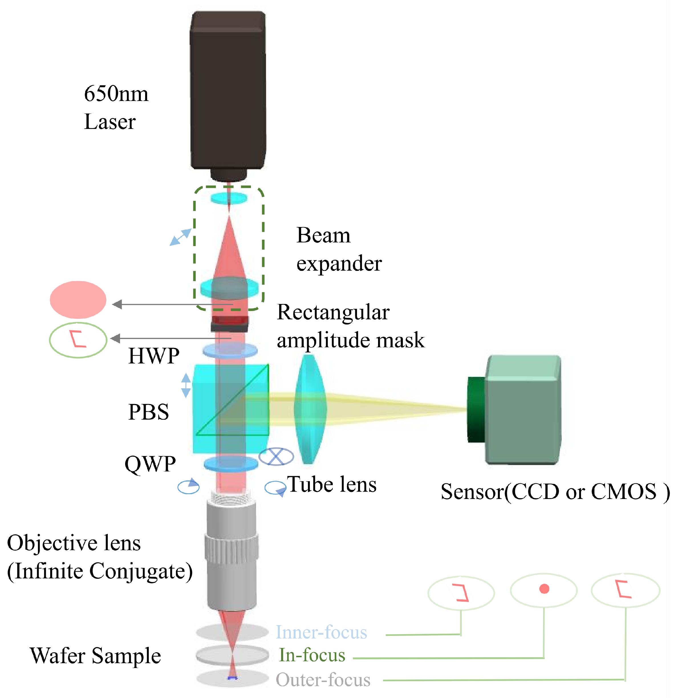
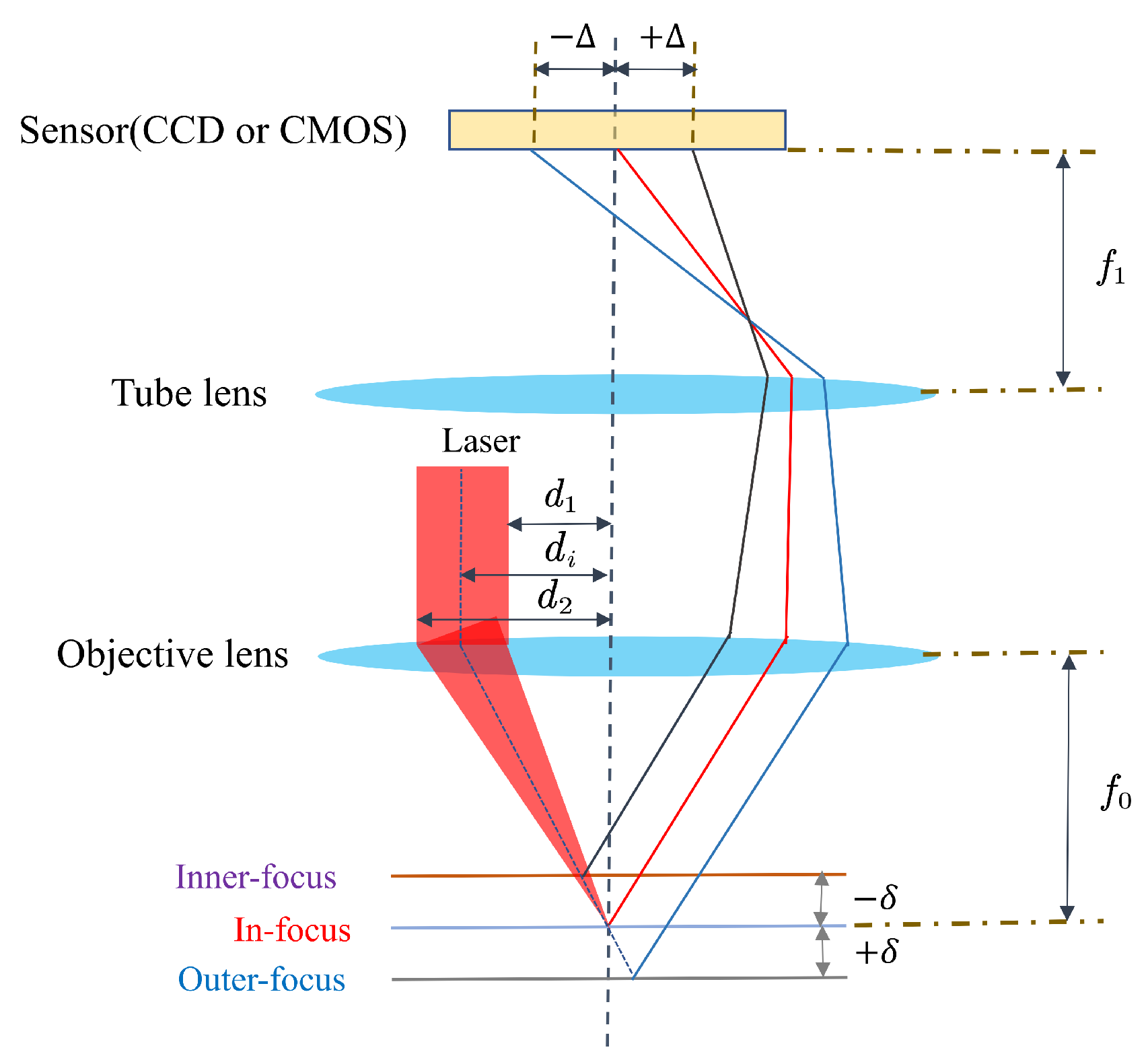
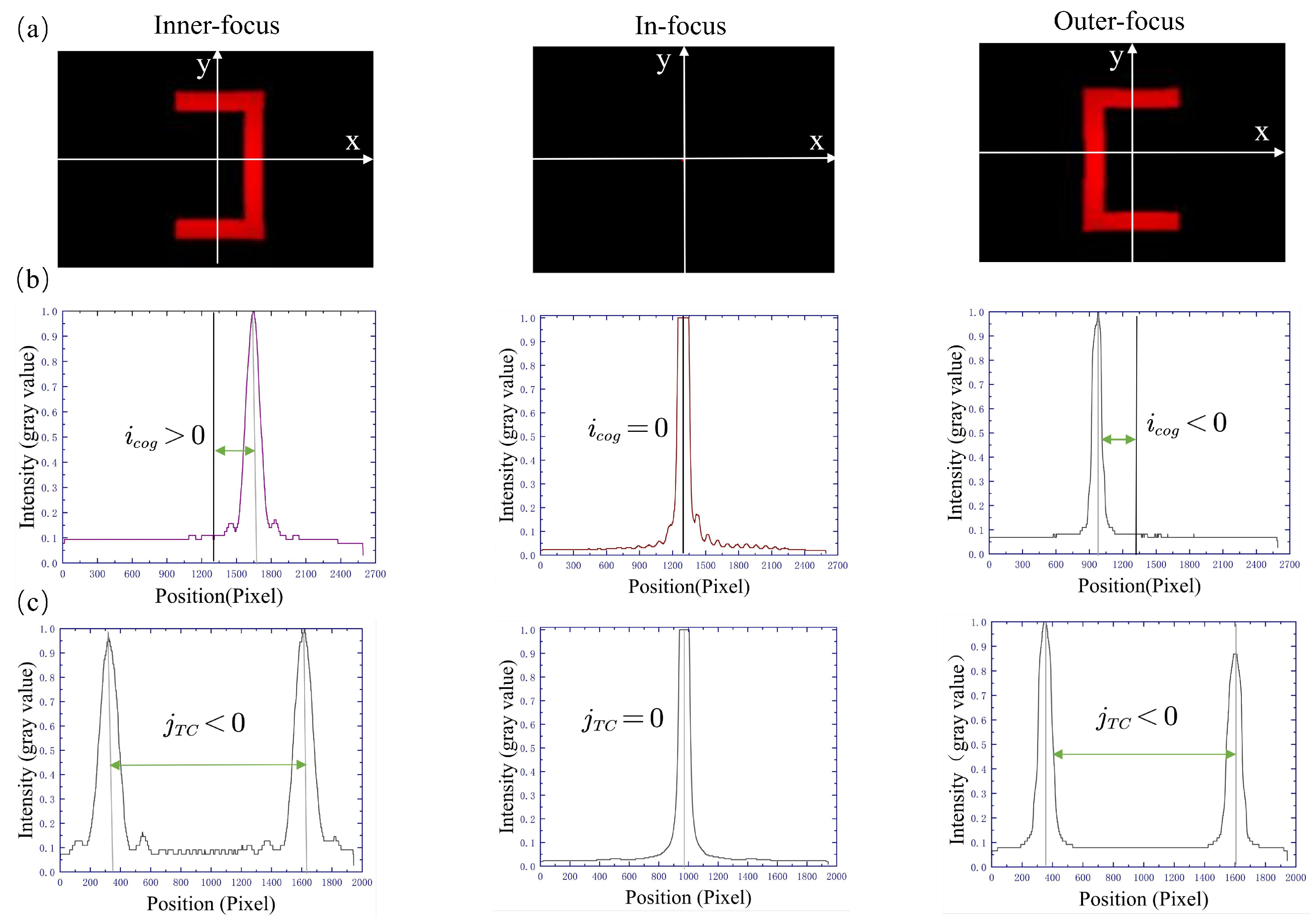
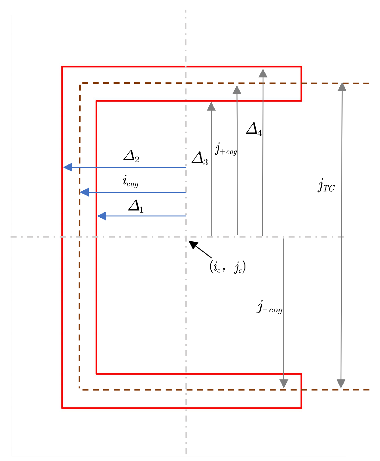
2. Methods
3. Results and Discussion
3.1. Simulation Analysis
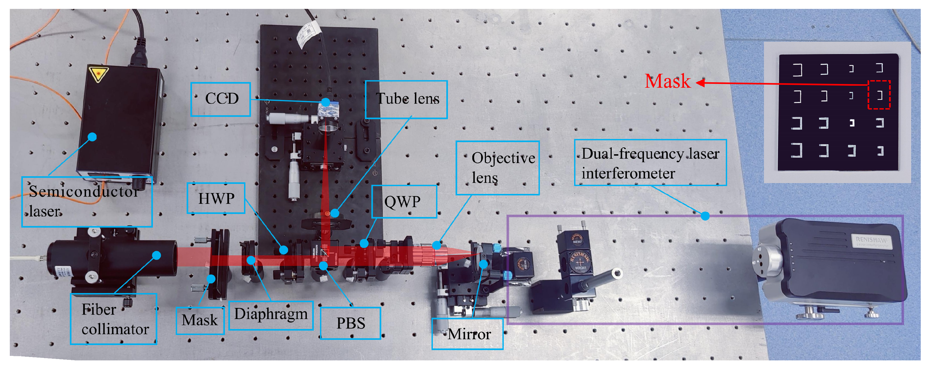
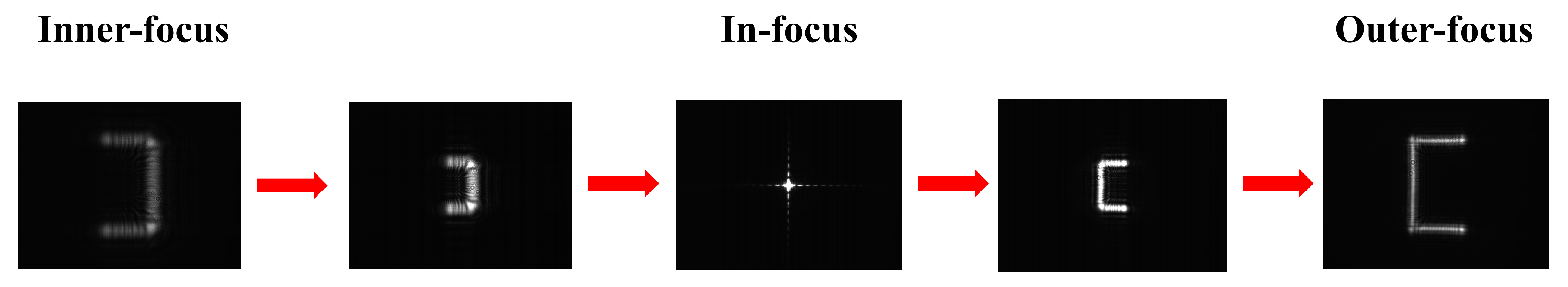
3.2. Experiment and Discussion
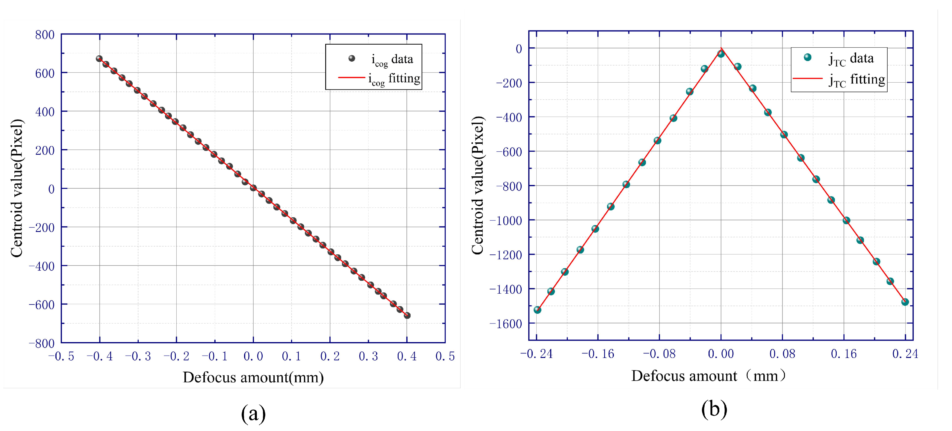
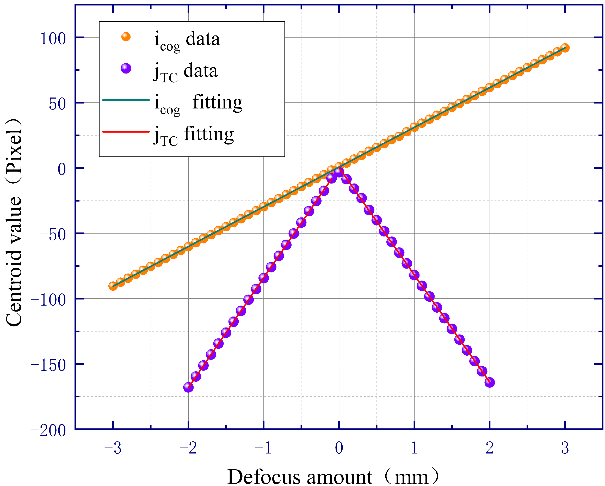
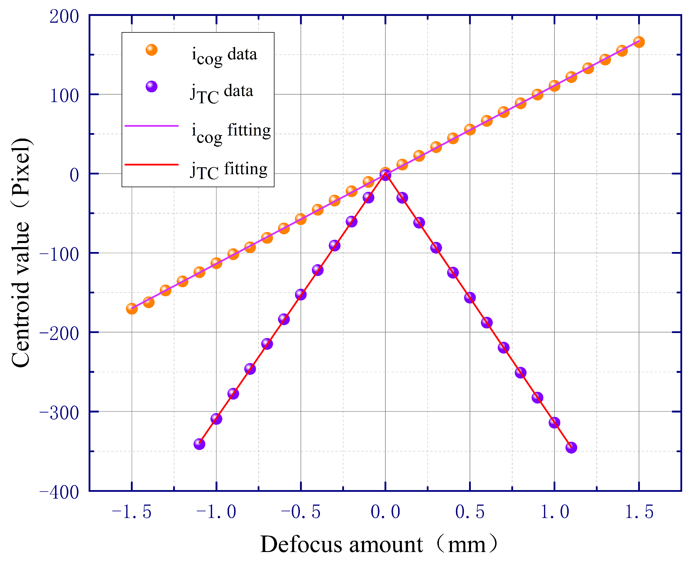
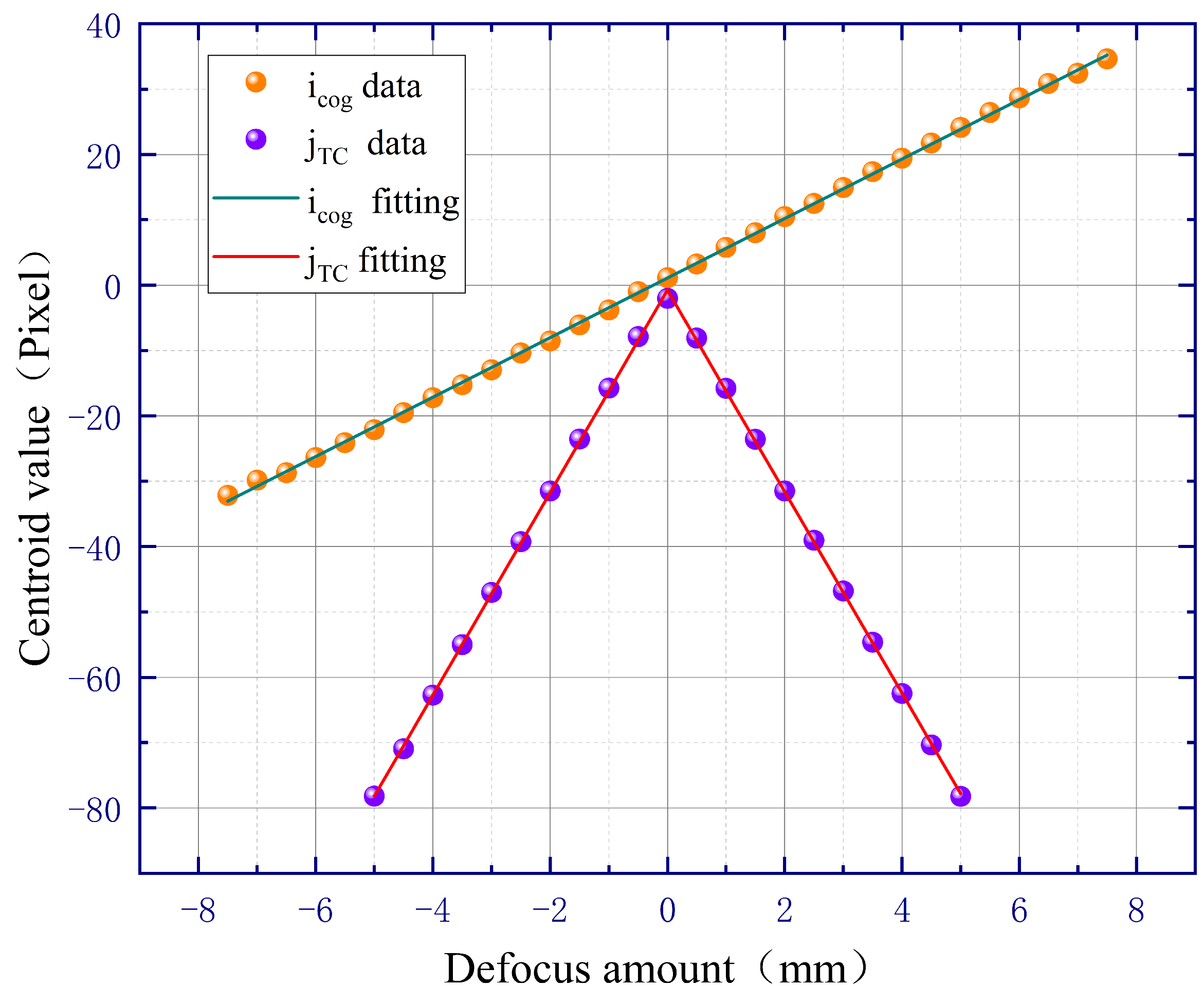
3.2.1. Verification of the Linear Relationship
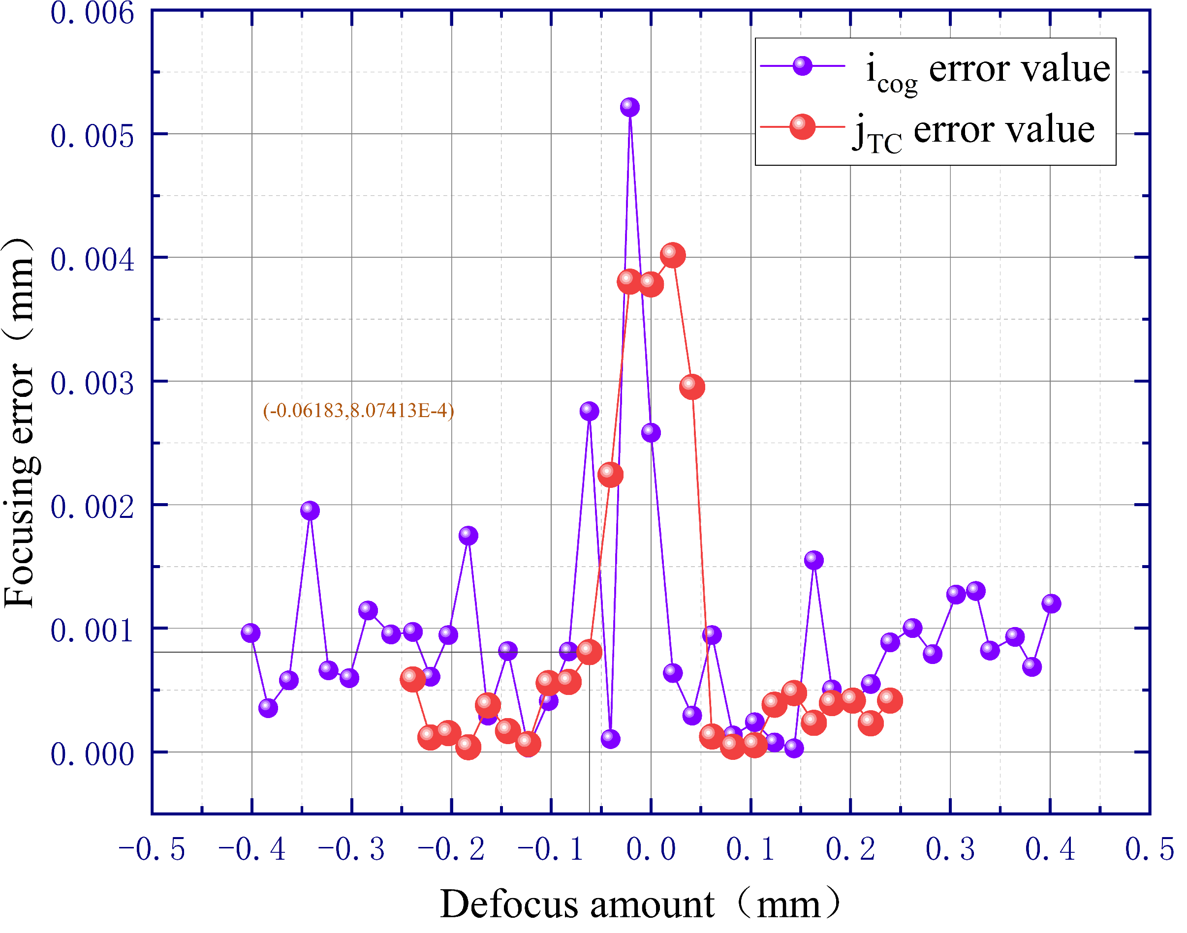
3.2.2. Measurement Error of the Defocus Amount
4. Conclusions
Author Contributions
Funding
Institutional Review Board Statement
Informed Consent Statement
Data Availability Statement
Conflicts of Interest
Abbreviations
| LED | Light-Emitting Diode |
| LCD | Liquid Crystal Display |
| OLED | Organic Light-Emitting Diode |
| CCD | Charge-Coupled Device |
| CMOS | Complementary Metal Oxide Semiconductor |
| PAF | Passive Auto-Focus |
| AAF | Active Auto-Focus |
| PBS | Polarization Beam Splitter |
| HWP | Half-Wave Plate |
| QWP | Quarter-Wave Plate |
References
- Wu, T.; Sher, C.W.; Lin, Y.; Lee, C.F.; Liang, S.; Lu, Y.; Chen, Z. Mini-LED and micro-LED: Promising candidates for the next generation display technology. Appl. Sci. 2018, 8, 1557. [Google Scholar] [CrossRef]
- Lee, V.W.; Twu, N.; Kymissis, I. Micro-LED technologies and applications. Inf. Disp. 2016, 32, 16–23. [Google Scholar] [CrossRef]
- Wu, Y.; Ma, J.; Su, P.; Zhang, L.; Xia, B. Full-color realization of micro-LED displays. Nanomaterials 2020, 10, 2482. [Google Scholar] [CrossRef]
- Liu, M.; Nie, J.; Liu, Y.; Sun, J.; Li, M.; Yan, C.; Yan, Q. Research on the reliability of Micro LED high-density solder joints under thermal cycling conditions. J. Physics Conf. Ser. 2022, 2221, 012010. [Google Scholar] [CrossRef]
- Anwar, A.R.; Sajjad, M.T.; Johar, M.A.; Hernández-Gutiérrez, C.A.; Usman, M.; Łepkowski, S.P. Recent progress in micro-LED-based display technologies. Laser Photonics Rev. 2022, 16, 2100427. [Google Scholar] [CrossRef]
- Zhou, X.; Tian, P.; Sher, C.W.; Wu, J.; Liu, H.; Liu, R.; Kuo, H.C. Growth, transfer printing and colour conversion techniques towards full-colour micro-LED display. Prog. Quantum Electron. 2020, 71, 100263. [Google Scholar] [CrossRef]
- Chen, D.; Chen, Y.C.; Zeng, G.; Zhang, D.W.; Lu, H.L. Integration Technology of Micro-LED for Next-Generation Display. Researh 2023, 6, 0047. [Google Scholar] [CrossRef]
- Kehtarnavaz, N.; Oh, H.J. Development and real-time implementation of a rule-based auto-focus algorithm. Real-Time Imaging 2003, 9, 197–203. [Google Scholar] [CrossRef]
- LeSage, A.J.; Kron, S.J. Design and implementation of algorithms for focus automation in digital imaging time-lapse microscopy. Cytom. J. Int. Soc. Anal. Cytol. 2002, 49, 159–169. [Google Scholar] [CrossRef]
- Wei, L.; Roberts, E. Neural network control of focal position during time-lapse microscopy of cells. Sci. Rep. 2018, 8, 7313. [Google Scholar] [CrossRef] [PubMed]
- Ren, Z.; Lam, E.Y.; Zhao, J. Acceleration of autofocusing with improved edge extraction using structure tensor and Schatten norm. Opt. Express 2020, 28, 14712–14728. [Google Scholar] [CrossRef] [PubMed]
- DiMeo, P.; Sun, L.; Du, X. Fast and accurate autofocus control using Gaussian standard deviation and gradient-based binning. Opt. Express 2021, 29, 19862–19878. [Google Scholar] [CrossRef]
- Zhang, C.; Jia, D.; Wu, N.; Guo, Z.; Ge, H. Autofocus method based on multi regions of interest window for cervical smear images. Multimed. Tools Appl. 2022, 81, 18783–18805. [Google Scholar] [CrossRef]
- Gu, C.C.; Cheng, H.; Wu, K.J.; Zhang, L.J.; Guan, X.P. A high precision laser-based autofocus method using biased image plane for microscopy. J. Sens. 2018, 2018, 8542680. [Google Scholar] [CrossRef]
- Liu, C.S.; Song, R.C.; Fu, S.J. Design of a laser-based autofocusing microscope for a sample with a transparent boundary layer. Appl. Phys. B 2019, 125, 1–12. [Google Scholar] [CrossRef]
- Cui, H.; Cui, D. Centroid-position-based autofocusing technique for Raman spectroscopy. Opt. Express 2019, 27, 27354–27368. [Google Scholar] [CrossRef]
- Bathe-Peters, M.; Annibale, P.; Lohse, M.J. All-optical microscope autofocus based on an electrically tunable lens and a totally internally reflected IR laser. Opt. Express 2018, 26, 2359–2368. [Google Scholar] [CrossRef]
- Liu, C.S.; Hu, P.H.; Lin, Y.C. Design and experimental validation of novel optics-based autofocusing microscope. Appl. Phys. B 2012, 109, 259–268. [Google Scholar] [CrossRef]
- Du, J.L.; Yan, W.; Liu, L.W.; Li, F.X.; Peng, F.P.; Wang, S.M.; Wang, J. Focal surface detection of high numerical aperture objective lens based on differential astigmatic method. IEEE Photonics J. 2021, 13, 1–8. [Google Scholar] [CrossRef]
- Huang, X.; He, J.; Liu, Q.; Lu, J.; Zhang, H. Coarse-to-fine auto-focus method using a white-and-red light source for white-light scanning interferometers. Optik 2023, 276, 170634. [Google Scholar] [CrossRef]
- Du, J.; Li, F.; Peng, F.; Wang, S.; Yan, W. Large-range and high-precision autofocus method based on an annular DOE for a laser direct writing system. Optics Express 2022, 30, 6981–6990. [Google Scholar] [CrossRef] [PubMed]
- Stein, U. MATLAB. In Foundations of Computational Mathematics, Budapest 2011; Cambridge University Press: Cambridge, UK, 2012; Volume 403, p. 230. [Google Scholar]
- Saxena, C.; Kourav, D. Noises and image denoising techniques: A brief survey. Int. J. Emerg. Technol. Adv. Eng. 2014, 4, 878–885. [Google Scholar]
- Otsu, N. A threshold selection method from gray-level histograms. IEEE Trans. Syst. Man Cybern. 1979, 9, 62–66. [Google Scholar] [CrossRef]
- Vivekananthan, V.; Vignesh, R.; Vasanthaseelan, S.; Joel, E.; Kumar, K.S. Concrete bridge crack detection by image processing technique by using the improved OTSU method. Mater. Today Proc. 2023, 74, 1002–1007. [Google Scholar] [CrossRef]
- Huang, T.; Yang, G.J.T.G.Y.; Tang, G. A fast two-dimensional median filtering algorithm. IEEE Trans. Acoust. Speech Signal Process. 1979, 27, 13–18. [Google Scholar] [CrossRef]


Disclaimer/Publisher’s Note: The statements, opinions and data contained in all publications are solely those of the individual author(s) and contributor(s) and not of MDPI and/or the editor(s). MDPI and/or the editor(s) disclaim responsibility for any injury to people or property resulting from any ideas, methods, instructions or products referred to in the content. |
© 2023 by the authors. Licensee MDPI, Basel, Switzerland. This article is an open access article distributed under the terms and conditions of the Creative Commons Attribution (CC BY) license (https://creativecommons.org/licenses/by/4.0/).
Share and Cite
He, W.; Ma, Y.; Wang, W. Rectangular Amplitude Mask-Based Auto-Focus Method with a Large Range and High Precision for a Micro-LED Wafer Defects Detection System. Sensors 2023, 23, 7579. https://doi.org/10.3390/s23177579
He W, Ma Y, Wang W. Rectangular Amplitude Mask-Based Auto-Focus Method with a Large Range and High Precision for a Micro-LED Wafer Defects Detection System. Sensors. 2023; 23(17):7579. https://doi.org/10.3390/s23177579
Chicago/Turabian StyleHe, Wenjun, Yufeng Ma, and Wenbo Wang. 2023. "Rectangular Amplitude Mask-Based Auto-Focus Method with a Large Range and High Precision for a Micro-LED Wafer Defects Detection System" Sensors 23, no. 17: 7579. https://doi.org/10.3390/s23177579
APA StyleHe, W., Ma, Y., & Wang, W. (2023). Rectangular Amplitude Mask-Based Auto-Focus Method with a Large Range and High Precision for a Micro-LED Wafer Defects Detection System. Sensors, 23(17), 7579. https://doi.org/10.3390/s23177579