
Configurable Encryption and Decryption Architectures for CKKS-Based Homomorphic Encryption


Abstract
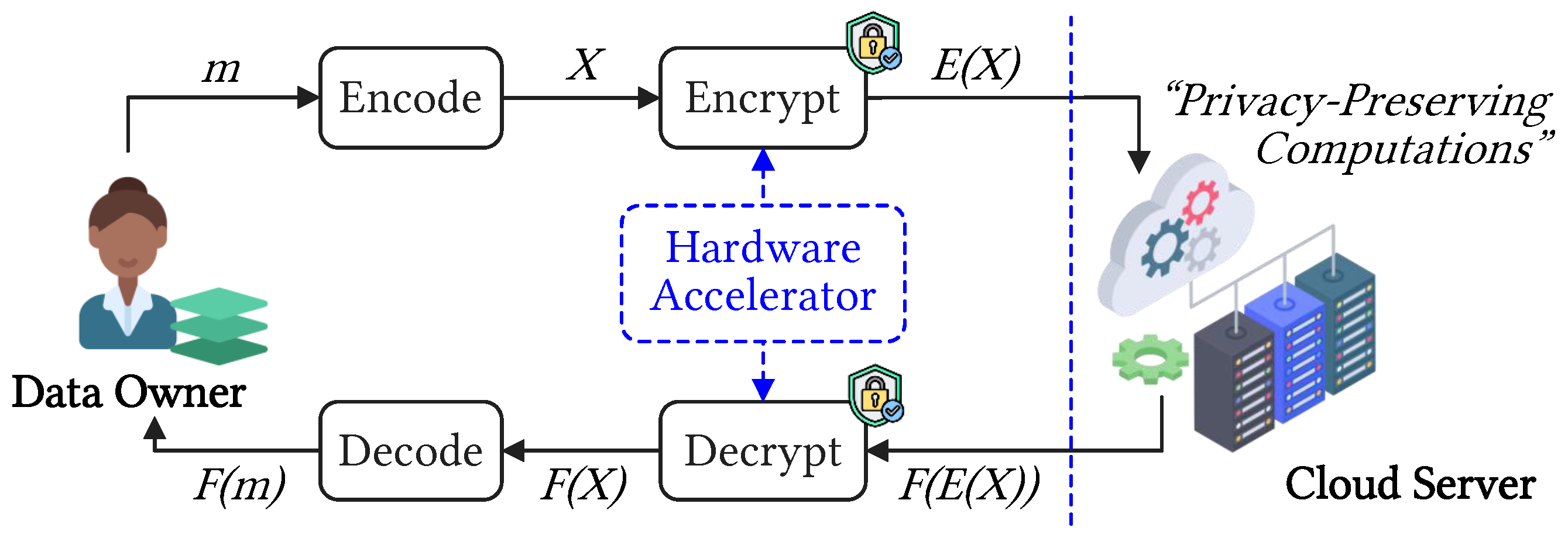
:1. Introduction
1.1. Related Works
1.2. Our Contributions
2. Background
2.1. Residue Number System (RNS)
2.2. Key Generation
2.3. Enryption and Decryption Algorithms
| Algorithm 1 CKKS-supported encryption implementation in SEAL [16] |
| Input: public key , encoded message , vector , errors . Output: ciphertext . 1: NTT NTT NTT 2: 3: ModSwitch; ModSwitch 4: return |
| Algorithm 2 CKKS-supported decryption implementation in SEAL [16] |
| Input: ciphertext , secret key . Output: approximate message 1: 2: return |
3. Recommended Parameters for HE Schemes and Our Selection
4. Proposed Configurable CKKS-Supported ENC-DEC Architectures
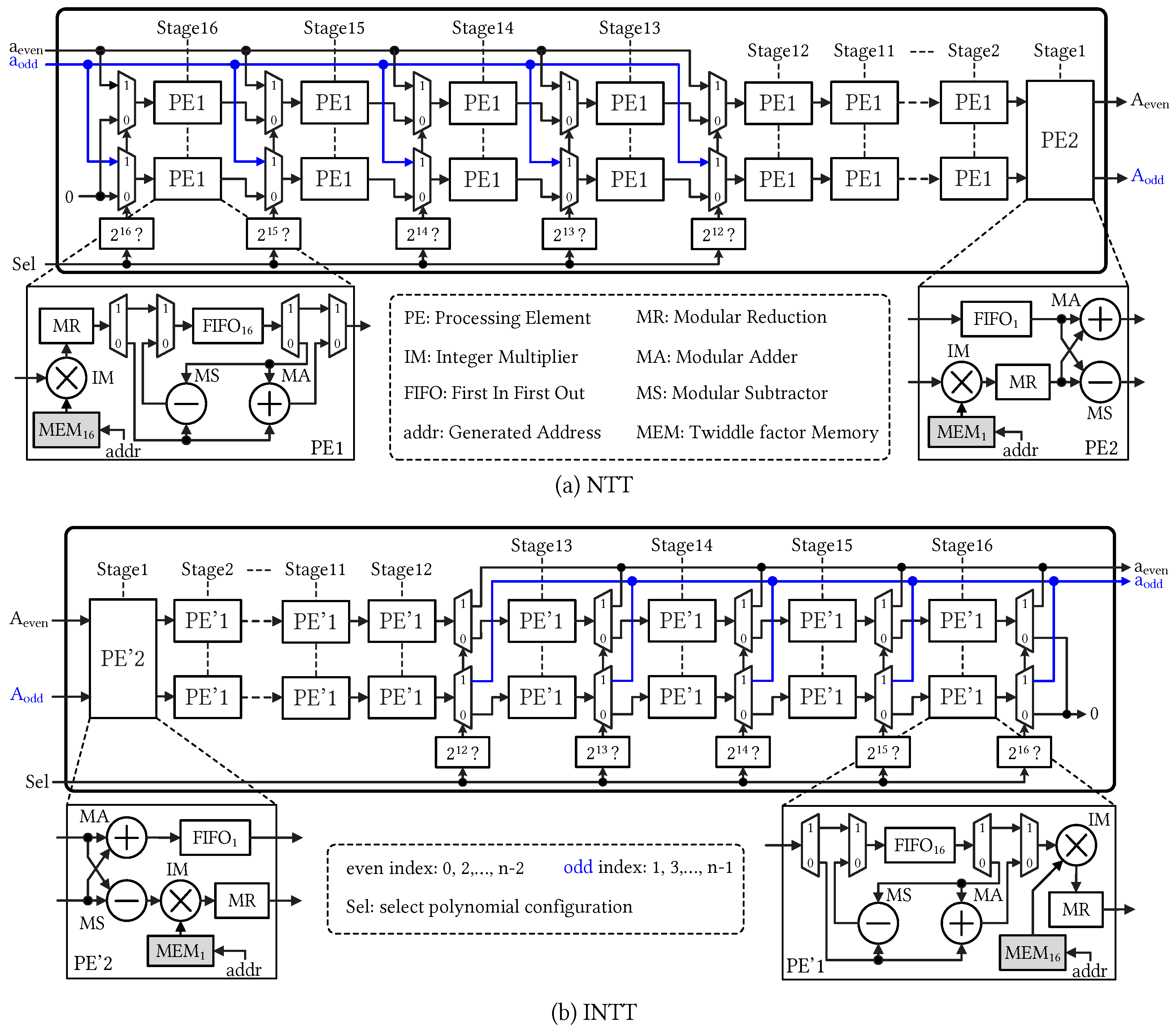
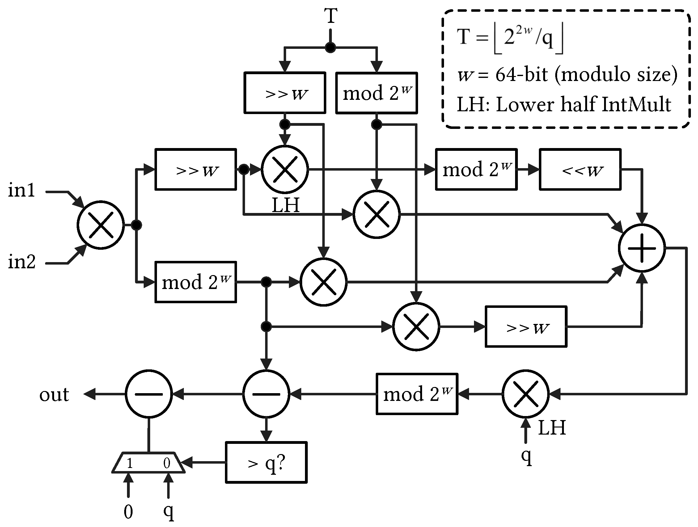
4.1. Proposed Configurable NTT and INTT Architectures
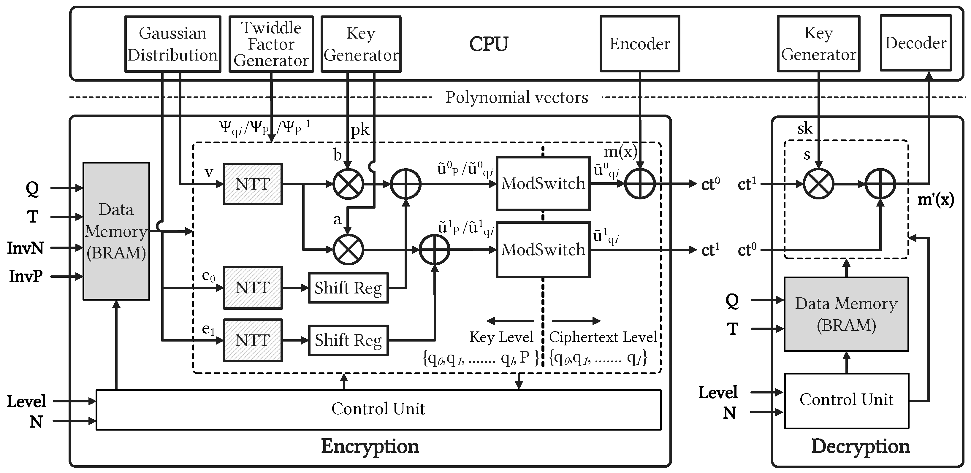
4.2. Proposed Configurable ENC-DEC Architectures
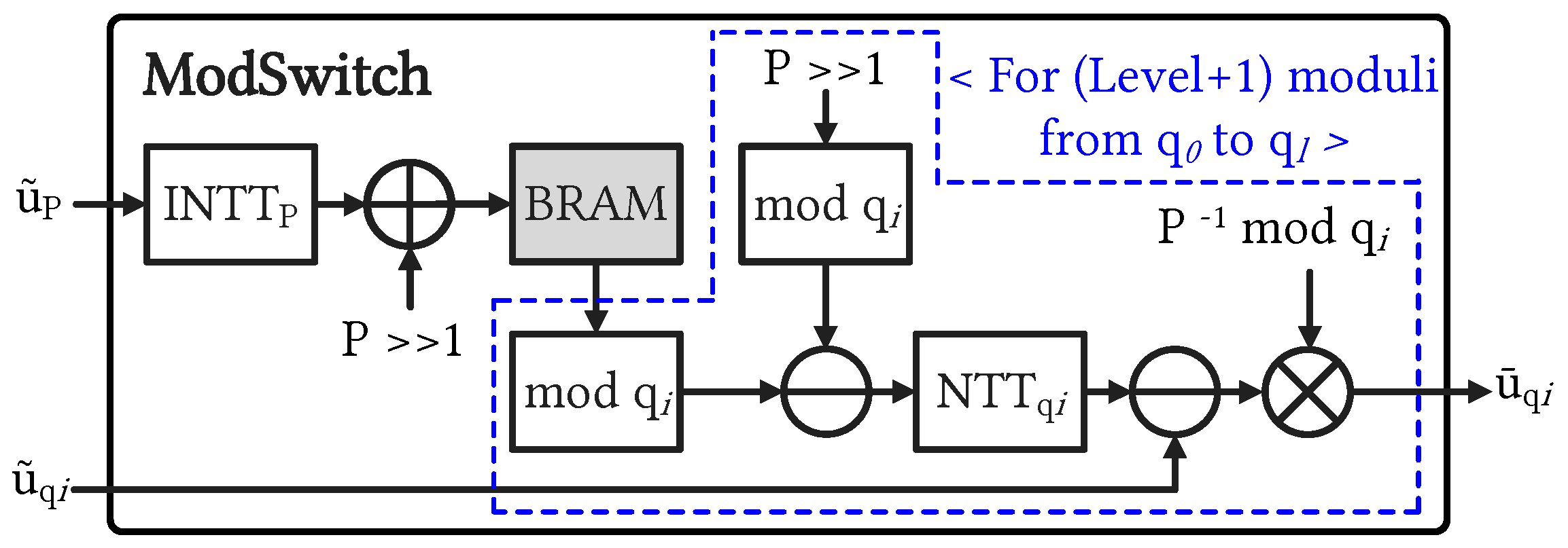
4.2.1. ModSwitch Unit
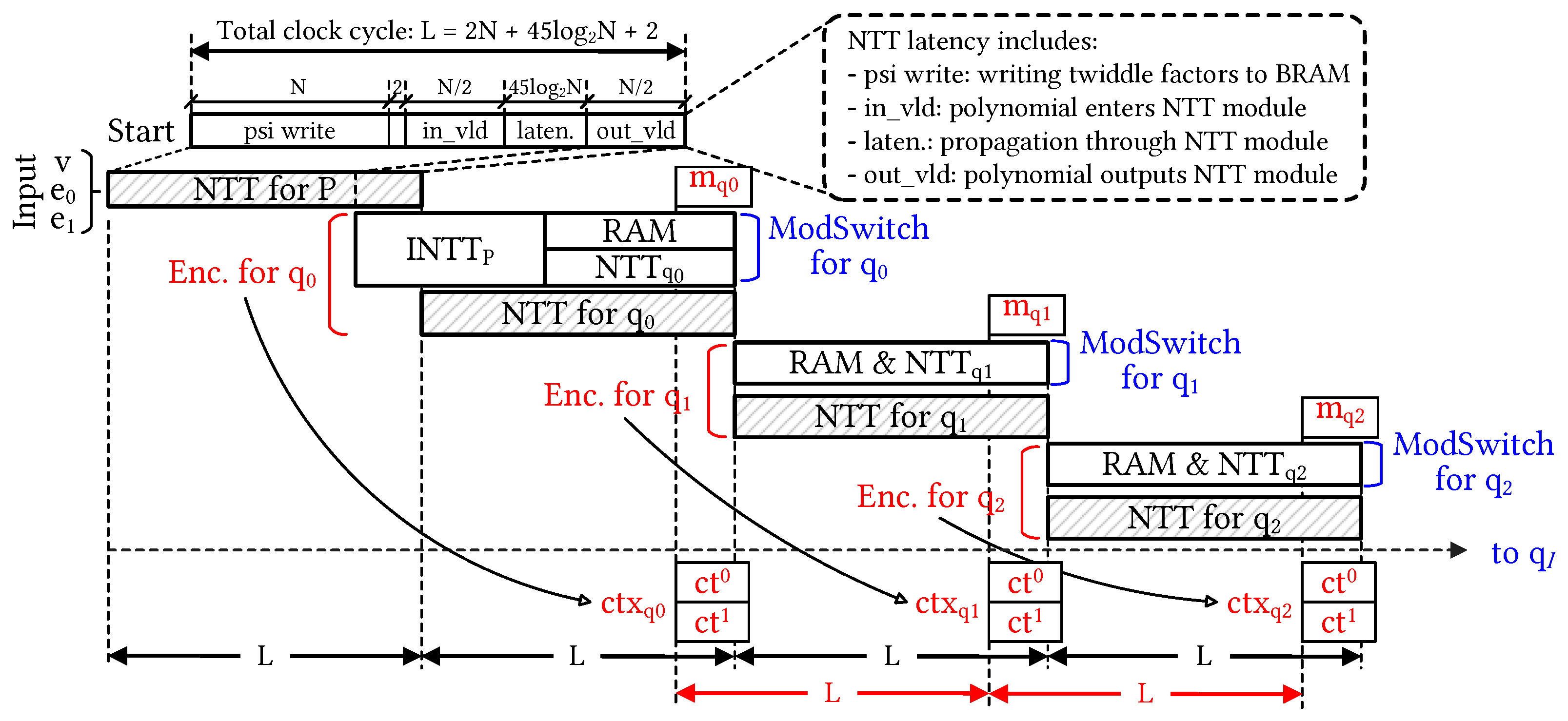
4.2.2. Controller and Timing Diagram
5. Evaluation Results and Discussion
6. Conclusions
Author Contributions
Funding
Institutional Review Board Statement
Informed Consent Statement
Data Availability Statement
Conflicts of Interest
References
- Rivest, R.L.; Adleman, L.; Dertouzos, M.L. On data banks and privacy homomorphisms. Found. Comput. Decis. Sci. 1978, 4, 169–180. [Google Scholar]
- Lyubashevsky, V.; Peikert, C.; Regev, O. On ideal lattices and learning with errors over rings. J. ACM 2013, 60, 1–35. [Google Scholar] [CrossRef]
- Çetin, G.S.; Savaş, E.; Sunar, B. Homomorphic sorting with better scalability. IEEE Trans. Parallel Distrib. Syst. 2021, 32, 760–771. [Google Scholar] [CrossRef]
- Cheon, J.H.; Han, K.; Kim, A.; Kim, M.; Song, Y. A full RNS variant of approximate homomorphic encryption. In Proceedings of the Selected Areas in Cryptography–SAC 2018: 25th International Conference, Calgary, AB, Canada, 15–17 August 2018; pp. 347–368. [Google Scholar] [CrossRef]
- Mert, A.C.; Öztürk, E.; Savaş, E. Design and implementation of encryption/decryption architectures for BFV homomorphic encryption scheme. IEEE Trans. Very Large Scale Integr. 2019, 28, 353–362. [Google Scholar] [CrossRef]
- Natarajan, D.; Dai, W. Seal-embedded: A homomorphic encryption library for the internet of things. IACR Trans. Cryptogr. Hardw. Embed. Syst. 2021, 9, 756–779. [Google Scholar] [CrossRef]
- van der Hagen, M.; Lucia, B. Client-optimized algorithms and acceleration for encrypted compute offloading. In Proceedings of the 27th ACM International Conference on Architectural Support for Programming Languages and Operating Systems, Lausanne, Switzerland, 28 Febrary–4 March 2022; pp. 683–696. [Google Scholar] [CrossRef]
- Azad, Z.; Yang, G.; Agrawal, R.; Petrisko, D.; Taylor, M.; Joshi, A. RACE: RISC-V SoC for En/Decryption Acceleration on the Edge for Homomorphic Computation. In Proceedings of the ACM/IEEE International Symposium on Low Power Electronics and Design, Boston, MA, USA, 1–3 August 2022; pp. 1–6. [Google Scholar] [CrossRef]
- Nguyen, T.T.; Kim, J.; Lee, H. CKKS-Based Homomorphic Encryption Architecture using Parallel NTT Multiplier. In Proceedings of the 2023 IEEE International Symposium on Circuits and Systems (ISCAS), Monterey, CA, USA, 21–25 May 2023; pp. 1–4. [Google Scholar] [CrossRef]
- Cheon, J.H.; Kim, A.; Kim, M.; Song, Y. Homomorphic Encryption for Arithmetic of Approximate Numbers. In Proceedings of the Advances in Cryptology–ASIACRYPT 2017: 23rd International Conference on the Theory and Applications of Cryptology and Information Security, Hong Kong, China, 3–7 December 2017; pp. 409–437. [Google Scholar] [CrossRef]
- Crandall, R.; Pomerance, C. Prime Numbers: A Computational Perspective, 2nd ed.; Springer: New York, NY, USA, 2005; pp. 83–115. [Google Scholar] [CrossRef]
- Fan, J.; Vercauteren, F. Somewhat practical fully homomorphic encryption. IACR Cryptol. Eprint Arch. 2012, 144, 1–19. [Google Scholar]
- Brakerski, Z. Fully homomorphic encryption without modulus switching from classical GapSVP. In Proceedings of the Advances in Cryptology–CRYPTO 2012: 32nd Annual Cryptology Conference, Santa Barbara, CA, USA, 19–23 August 2012; pp. 868–886. [Google Scholar] [CrossRef]
- Brakerski, Z.; Gentry, C.; Vaikuntanathan, V. (Leveled) fully homomorphic encryption without bootstrapping. ACM Trans. Comput. Theory 2014, 6, 1–36. [Google Scholar] [CrossRef]
- Duong-Ngoc, P.; Kwon, S.; Yoo, D.; Lee, H. Area-efficient number-theoretical transform architecture for Homomorphic encryption. IEEE Trans. Circuits Syst. I Regul. Pap. 2023, 70, 1270–1283. [Google Scholar] [CrossRef]
- Microsoft SEAL (Release 4.0). Microsoft Research. Available online: https://github.com/Microsoft/SEAL (accessed on 14 February 2023).
- Albrecht, M.; Chase, M.; Chen, H.; Ding, J.; Goldwasser, S.; Gorbunov, S.; Halevi, S.; Hoffstein, J.; Laine, K.; Lauter, K.; et al. Homomorphic encryption standards. In Protecting Privacy through Homomorphic Encryption; Lauter, K., Dai, W., Laine, K., Eds.; Springer: Cham, Switzerland, 2022; pp. 31–62. [Google Scholar] [CrossRef]
- Duong, P.N.; Lee, H. Pipelined Key Switching Accelerator Architecture for CKKS-Based Fully Homomorphic Encryption. Sensors 2023, 23, 4594. [Google Scholar] [CrossRef] [PubMed]
- Ye, Z.; Cheung, R.C.C.; Huang, K. PipeNTT: A Pipelined Number Theoretic Transform Architecture. IEEE Trans. Circuits Syst. II Express Briefs 2022, 69, 4068–4072. [Google Scholar] [CrossRef]
- Hirner, F.; Mert, A.C.; Roy, S.S. PROTEUS: A Tool to generate pipelined Number Theoretic Transform Architectures for FHE and ZKP applications. Cryptol. ePrint Arch. 2023. Available online: https://eprint.iacr.org/2023/267 (accessed on 20 August 2023).
- Kurniawan, S.; Duong-Ngoc, P.; Lee, H. Configurable Memory-Based NTT Architecture for Homomorphic Encryption. IEEE Trans. Circuits Syst. II Express Briefs 2023. [Google Scholar] [CrossRef]

| N | Recommended Parameter [17] () | Selected Parameter | |||
|---|---|---|---|---|---|
| 128 bits | 192 bits | 256 bits | Coefficient moduli (bits) | ||
| 109 | 75 | 58 | 2 | {30, 20, 20, 30} | |
| 218 | 152 | 118 | 5 | {30, 20, 20, 20, 20, 20, 30} | |
| 438 | 305 | 237 | 6 | {60, 48, 48, 48, 48, 48, 48, 60} | |
| 881 | 611 | 476 | 15 | {60, 48 (×15)…, 60} | |
| 1782 | 1242 | 963 | 30 | {60, 48 (×30)…, 60} | |
| Module | Resource Utilization | Freq. | Latency | |||
|---|---|---|---|---|---|---|
| LUT | FF | DSP | BRAM | (MHz) | (CC) | |
| NTT | 59,619 | 109,226 | 1984 | 240.5 | 250 | 33,488 |
| ⌊ MM | 1463 | 3339 | 64 | 0 | - | 42 |
| ⌊ MA | 195 | 0 | 0 | 0 | - | 1 |
| ⌊ MS | 97 | 0 | 0 | 0 | - | 1 |
| INTT | 65,291 | 115,323 | 2112 | 240.5 | 250 | 33,529 |
| Design | N | Max | FPGA Resource Utilization | Freq. | Latency | Thro. | Effi. | Device | ||||
|---|---|---|---|---|---|---|---|---|---|---|---|---|
| (bits) | LUT | FF | DSP | BRAM | E.S ‡ | (MHz) | (μs) | (Mbps) | () | |||
| [19]’22 | 60 | 17K | 11K | 286 | 100 | 38.7K | 150 | 55 | 4450 | 0.11 | XV485 | |
| [20]’23 | 64 | 31.3K | 24.4K | 300 | 255 | 97.8K | 150 | 221 | 19,009 | 0.19 | XV485 | |
| [21]’23 | 60 | 74.5K | 61.4K | 288 | 155 | 49.7K | 250 | 66.5 | 59,120 | 1.19 | VU37P | |
| 10 | 26,214 | 0.19 | ||||||||||
| 19 | 27,594 | 0.20 | ||||||||||
| Ours | 64 | 59.6K | 109.2K | 1984 | 240.5 | 137K | 250 | 35 | 29,959 | 0.22 | XCU250 | |
| 68 | 30,841 | 0.23 | ||||||||||
| 134 | 31,301 | 0.23 | ||||||||||
| Parameter | Encryption (ops) | Decryption (ops) | |||
|---|---|---|---|---|---|
| N | Level | Intel Core-i7 | XCU250 (Speedup) | Intel Core-i7 | XCU250 (Speedup) |
| 2 | 377 | 14,493 (×38.4) | 16,631 | 62,500 (×3.8) | |
| 5 | 123 | 2950 (×24.0) | 4460 | 12,195 (×2.7) | |
| 6 | 60 | 1249 (×20.8) | 1686 | 5076 (×3.0) | |
| 15 | 13 | 251 (×19.3) | 379 | 1015 (×2.7) | |
| 30 | 4 | 64 (×16.0) | 6 | 254 (×42.3) | |
| Parameter | Encryption | Decryption | |
|---|---|---|---|
| Design | [9]’23 | This work | This work |
| N | |||
| Level | 3 | 2∼30 | 2∼30 |
| LUT | 883K (51%) | 1179K (68%) | 10.7K (0.6%) |
| FF | 897K (26%) | 1036K (30%) | 6.9K (0.2%) |
| DSP | 6042 (58%) | 12,288 (100%) | 133 (1%) |
| BRAM | 1563 (49%) | 828.5 (31%) | 3 (0.1%) |
| Freq. (MHz) | 250 | 250 | 250 |
| Latency (s) | 102.1 | 16,869 § | 3937 § |
Disclaimer/Publisher’s Note: The statements, opinions and data contained in all publications are solely those of the individual author(s) and contributor(s) and not of MDPI and/or the editor(s). MDPI and/or the editor(s) disclaim responsibility for any injury to people or property resulting from any ideas, methods, instructions or products referred to in the content. |
© 2023 by the authors. Licensee MDPI, Basel, Switzerland. This article is an open access article distributed under the terms and conditions of the Creative Commons Attribution (CC BY) license (https://creativecommons.org/licenses/by/4.0/).
Share and Cite
Lee, J.; Duong, P.N.; Lee, H. Configurable Encryption and Decryption Architectures for CKKS-Based Homomorphic Encryption. Sensors 2023, 23, 7389. https://doi.org/10.3390/s23177389
Lee J, Duong PN, Lee H. Configurable Encryption and Decryption Architectures for CKKS-Based Homomorphic Encryption. Sensors. 2023; 23(17):7389. https://doi.org/10.3390/s23177389
Chicago/Turabian StyleLee, Jaehyeok, Phap Ngoc Duong, and Hanho Lee. 2023. "Configurable Encryption and Decryption Architectures for CKKS-Based Homomorphic Encryption" Sensors 23, no. 17: 7389. https://doi.org/10.3390/s23177389
APA StyleLee, J., Duong, P. N., & Lee, H. (2023). Configurable Encryption and Decryption Architectures for CKKS-Based Homomorphic Encryption. Sensors, 23(17), 7389. https://doi.org/10.3390/s23177389