
A Detailed dSPACE-Based Implementation of Modulated Model Predictive Control for AC Microgrids


Abstract
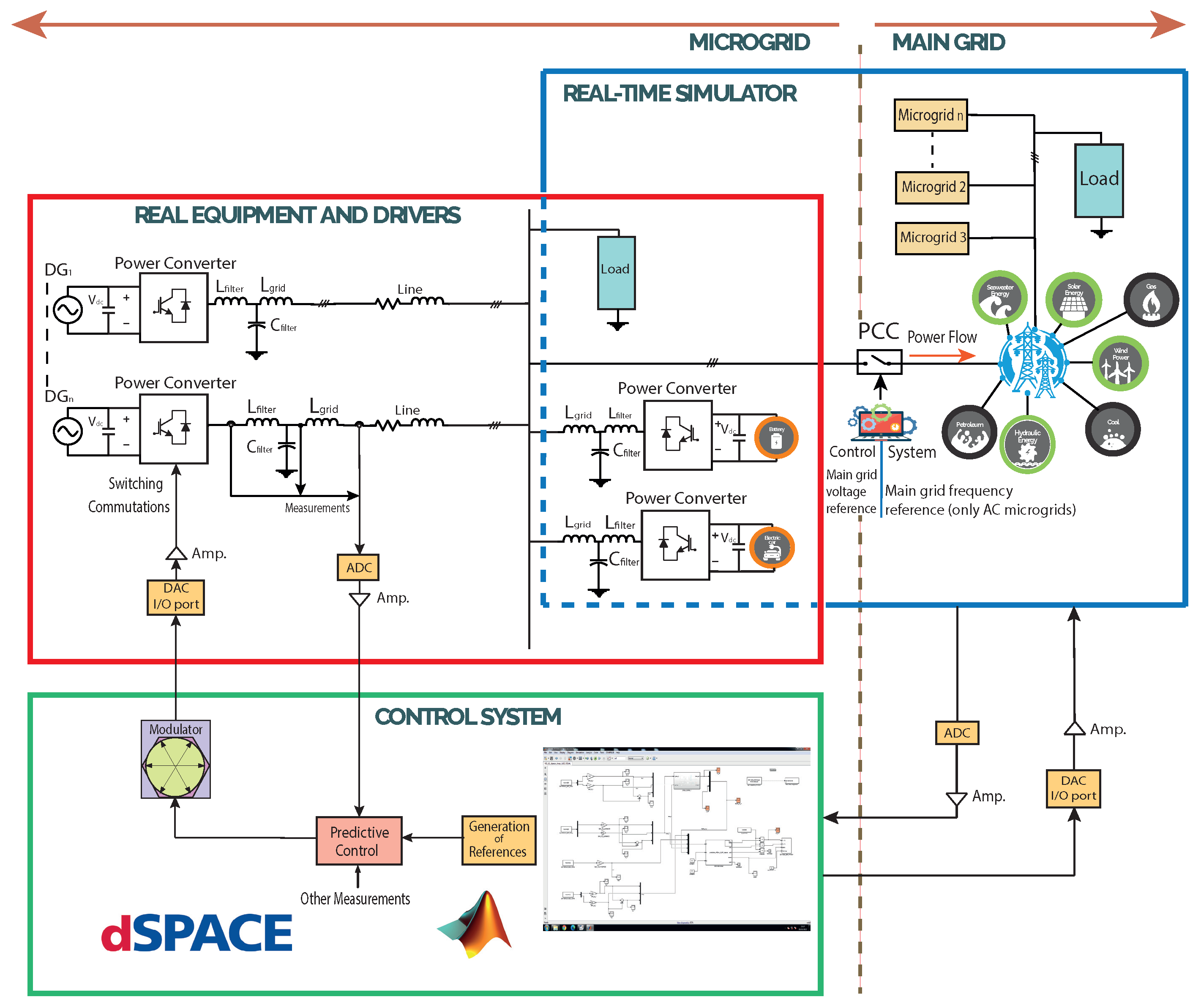
1. Introduction
2. Experimental System Description
2.1. Description of the Power Converter
Switches Characteristics
2.2. Filter
- = 2.0 mH;
- = 11 F;
- = 1.0 mH.
2.3. Load
- = 10 ;
- = 10 mH.
2.4. dSPACE ds1103 Control Platform
- The CP1103 connector panel provides useful connections between the ds1103 control platform and other equipment that will be connected to it;
- In addition to the connector panel, the dSPACE ds1103 considers additional connectors and a panel with an array of LEDs showing the states of the digital signals.
- Four ADCs with four multiplexed input signals each, from ADCH1 to ADCH16;
- Four parallel (non-multiplexed) ADCs with one input signal each, from ADCH17 to ADCH20.
2.5. Experimental Complete Setup
3. Implementation of the Controller
3.1. The Modulated Model Predictive Controller
3.2. MATLAB/Simulink Model
3.2.1. Modulated Model Predictive Control
3.2.2. Droop Control and Virtual Impedance
3.2.3. Analogue-to-Digital Converters
- ADCH1 and ADCH2, for and , respectively;
- ADCH3 and ADCH4, for and , respectively;
- ADCH13 and ADCH14, for and , respectively;
- ADCH15 for .
3.2.4. Interruption from the Slave DSP
3.2.5. Frequency Reference
3.3. FPGA
3.4. dSPACE Control Desk
3.5. Complete Model
4. Experimental Waveforms

| Parameter | Value |
|---|---|
| DC link voltage, | 30 V |
| Switching frequency (MPC) | 20 kHz |
| Sampling time, | 50 s |
| CF Weighting factors | = 40, = 20 |
| filter | = 2.0 mH, = 11 F, = 1.0 mH |
| Load | = 10 , = 10 mH |
| Nominal voltage | = 15 V, = Hz |
| Droop coefficients | = 0.0015 V/W, = 0.0025 rad/sVar |
| Line impedance | = 0.1 , = 1.114 mH |
| Virtual resistance | = 2 |
5. Discussion
5.1. Experimental Waveforms
- The capacitor voltage for phase a, , in Figure 22 and Figure 23a, was controlled as expected, but the presence of resonant noise can be seen. Resonance is known to be an inherent problem with filters. As mentioned earlier in this article, the use of filters was based on the availability of equipment in the laboratory; therefore, from these designs, the size of the capacitor had to be increased, from 1 F to 11 F, because, experimentally, an excess of resonance appeared;
- This resonance was produced by the parasitic components in the filters and in the semiconductor components (MOSFETs) of the experimental setup. Additionally, the fact that, as a contributor to this resonance in the capacitor voltage waveform, the delay provided by the drivers and the elements of the trigger pulse appeared;
- As shown in Figure 23b, the THD value was ≈ 6.6%, and was within the established standard deviation limits of 519–2014;
- The THD of the capacitor voltage, , the harmonics spectrum, was not spread across the frequencies, as mentioned earlier as the main drawback of not fixing the frequency.
- The waveforms of the output currents, , are shown in Figure 23c;
- Spectra analysis is shown in Figure 23d, in which it can be seen that the low-frequency harmonics in the currents (500 Hz) may have been occasioned by the unbalance among the filters and the load;
- The harmonics content was in the proximity of the limits of the 51st harmonics, with the currents having less distortion (≈2.8%), with attenuated high frequencies, by the filter inductances and the microgrid system.
5.2. dSPACE Implementation
6. Conclusions
Author Contributions
Funding
Conflicts of Interest
Abbreviations
| AC | alternating current |
| PCC | point of common coupling |
| MPC | modulated model predictive control |
| VSI | voltage source inverter |
| MPC | model predictive control |
| FS-MPC | finite-set model predictive control |
| DG | distributed generator |
| DER | distributed energy resource |
| MG | microgrid |
| HIL | hardware-in-the-loop |
| PID | proportional–integral–differential |
| PI | proportional–integral |
| RT-LAB | real-time laboratory |
| MPC | modified modulated model predictive control |
| DFIG | doubly fed induction generator |
| RTI | real-time interface |
| SVM | space vector modulation |
| PWMSV | pulse-width modulation space vector |
| PWMINT | pulse-width modulation interruption |
| HWINT | hardware (external) interruption |
| CF | cost function |
| NPC | neutral-point-clamped |
| LCL | inductor–capacitor–inductor |
| MOSFET | metal-oxide-semiconductor field-effect transistor |
| PWM | pulse-width modulation |
| DC | direct current |
| RL | resistor–inductor |
| DSP | digital signal processor |
| THD | total harmonic distortion |
| FPGA | field-programmable gate array |
| I/O | input–output |
| ADC | analogue-to-digital-converter |
| DAC | digital-to-analogue-converter |
| LED | light-emitting diode |
| PLL | phase-locked loop |
| PCB | printed circuit board |
| RMS | root mean square |
| LERAE | laboratory of renewable energy and electrical conditioning |
| DESS | distributed energy storage system |
Appendix A. Code of the Modulated Predictive Controller and the Dead-Times Generation with the Atlys FPGA
Appendix A.1. Code of the Modulated Model Predictive Control
Appendix A.2. Code of Dead-Times in the Atlys FPGA for the First Leg of the Two-Level, Three-Phase VSI
References
- Nigam, S.; Ajala, O.; Dominguez-Garcia, A.D. A Controller Hardware-in-the-Loop Testbed: Verification and Validation of Microgrid Control Architectures. IEEE Electrif. Mag. 2020, 8, 92–100. [Google Scholar] [CrossRef]
- IEA. Unlocking the Potential of Distributed Energy Resources Power System Opportunities and Best Practices; International Energy Agency: Paris, France, 2022; pp. 1–116. [Google Scholar]
- Lei, M.; Yang, Z.; Wang, Y.; Xu, H.; Meng, L.; Vasquez, J.C.; Guerrero, J.M. An MPC-Based ESS Control Method for PV Power Smoothing Applications. IEEE Trans. Power Electron. 2018, 33, 2136–2144. [Google Scholar] [CrossRef]
- Arani, M.F.M.; Mohamed, Y.A.R.I. Dynamic droop control for wind turbines participating in primary frequency regulation in microgrids. IEEE Trans. Smart Grid 2018, 9, 5742–5751. [Google Scholar] [CrossRef]
- Sun, L.; Wu, G.; Xue, Y.; Shen, J.; Li, D.; Lee, K.Y. Coordinated control strategies for fuel cell power plant in a microgrid. IEEE Trans. Energy Convers. 2018, 33, 1–9. [Google Scholar] [CrossRef]
- Villalón, A.; Rivera, M.; Salgueiro, Y.; Muñoz, J.; Dragičević, T.; Blaabjerg, F. Predictive control for microgrid applications: A review study. Energies 2020, 13, 2454. [Google Scholar] [CrossRef]
- Villalón, A.; Muñoz, C.; Aliaga, R.; Muñoz, J.; Rivera, M.; Zanchetta, P. Power Sharing Control of Islanded AC Microgrid Considering Droop Control and Virtual Impedance. In Proceedings of the 2020 IEEE International Conference on Industrial Technology (ICIT), Buenos Aires, Argentina, 26–28 February 2020; pp. 1139–1144. [Google Scholar] [CrossRef]
- Mannini, R.; Eynard, J.; Grieu, S. A Survey of Recent Advances in the Smart Management of Microgrids and Networked Microgrids. Energies 2022, 15, 7009. [Google Scholar] [CrossRef]
- Hou, X.; Sun, Y.; Lu, J.; Zhang, X.; Koh, L.H.; Su, M.; Guerrero, J.M. Distributed hierarchical control of AC microgrid operating in grid-connected, islanded and their transition modes. IEEE Access 2018, 6, 77388–77401. [Google Scholar] [CrossRef]
- Milczarek, A.; Malinowski, M.; Guerrero, J.M. Reactive Power Management in Islanded Microgrid - Proportional Power Sharing in Hierarchical Droop Control. IEEE Trans. Smart Grid 2015, 6, 1631–1638. [Google Scholar] [CrossRef]
- Mahmood, H.; Michaelson, D.; Jiang, J. Accurate reactive power sharing in an islanded microgrid using adaptive virtual impedances. IEEE Trans. Power Electron. 2015, 30, 1605–1617. [Google Scholar] [CrossRef]
- Zhang, C.; Guerrero, J.M.; Vasquez, J.C.; Coelho, E.A.A. Control Architecture for Parallel-Connected Inverters in Uninterruptible Power Systems. IEEE Trans. Power Electron. 2016, 31, 5176–5188. [Google Scholar] [CrossRef]
- Zhang, M.; Song, B.; Wang, J. Circulating Current Control Strategy Based on Equivalent Feeder for Parallel Inverters in Islanded Microgrid. IEEE Trans. Power Syst. 2019, 34, 595–605. [Google Scholar] [CrossRef]
- Razmi, D.; Lu, T. A Literature Review of the Control Challenges of Distributed Energy Resources Based on Microgrids (MGs): Past, Present and Future. Energies 2022, 15, 4676. [Google Scholar] [CrossRef]
- Papadimitriou, C.N.; Zountouridou, E.I.; Hatziargyriou, N.D. Review of hierarchical control in DC microgrids. Electr. Power Syst. Res. 2015, 122, 159–167. [Google Scholar] [CrossRef]
- Hossain, M.A.; Pota, H.R.; Issa, W.; Hossain, M.J. Overview of AC microgrid controls with inverter-interfaced generations. Energies 2017, 10, 1300. [Google Scholar] [CrossRef]
- Degner, T.; Soultanis, N.; Engler, A.; Gil de Muro, A. Intelligent local controllers. In Microgrids: Architectures and Control, 1st ed.; Hatziargyriou, N., Ed.; Wiley—IEEE Press: Chichester, UK, 2014; Chapter Intelligent Local Controllers; pp. 81–116. [Google Scholar] [CrossRef]
- Abbasi, M.; Abbasi, E.; Li, L.; Aguilera, R.P.; Lu, D.; Wang, F. Review on the Microgrid Concept, Structures, Components, Communication Systems, and Control Methods. Energies 2023, 16, 484. [Google Scholar] [CrossRef]
- Vandoorn, T.; Kooning, J.D.; Meersman, B.; Vandevelde, L. Review of primary control strategies for islanded microgrids with power-electronic interfaces. Renew. Sustain. Energy Rev. 2013, 19, 613–628. [Google Scholar] [CrossRef]
- Babayomi, O.; Zhang, Z.; Dragicevic, T.; Hu, J.; Rodriguez, J. Smart grid evolution: Predictive control of distributed energy resources—A review. Int. J. Electr. Power Energy Syst. 2023, 147, 108812. [Google Scholar] [CrossRef]
- Donoso, F.; Mora, A.; Cardenas, R.; Angulo, A.; Saez, D.; Rivera, M. Finite-Set Model-Predictive Control Strategies for a 3L-NPC Inverter Operating with Fixed Switching Frequency. IEEE Trans. Ind. Electron. 2018, 65, 3954–3965. [Google Scholar] [CrossRef]
- Chen, T.; Abdel-Rahim, O.; Peng, F.; Wang, H. An Improved Finite Control Set-MPC-Based Power Sharing Control Strategy for Islanded AC Microgrids. IEEE Access 2020, 8, 52676–52686. [Google Scholar] [CrossRef]
- Bevrani, H.; Francois, B.; Ise, T. Microgrid Dynamics and Control, 1st ed.; John Wiley & Sons: Hoboken, NJ, USA, 2017; p. 684. [Google Scholar]
- Ren, W.; Steurer, M.; Baldwin, T.L. An effective method for evaluating the accuracy of power hardware-in-the-loop simulations. IEEE Trans. Ind. Appl. 2008, 45, 1484–1490. [Google Scholar] [CrossRef]
- Wang, Y.; Delille, G.; Guillaud, X.; Colas, F.; François, B. Real-time simulation: The missing link in the design process of advanced grid equipment. In Proceedings of the IEEE PES General Meeting, Minneapolis, MN, USA, 25–29 July 2010. [Google Scholar] [CrossRef]
- Youness, E.M.; Aziz, D.; Abdelaziz, E.G.; Jamal, B.; Najib, E.O.; Othmane, Z.; Khalid, M.; BOSSOUFI, B. Implementation and validation of backstepping control for PMSG wind turbine using dSPACE controller board. Energy Rep. 2019, 5, 807–821. [Google Scholar] [CrossRef]
- Mensou, S.; Essadki, A.; Nasser, T.; Idrissi, B.B.; Tarla, L.B. Dspace DS1104 implementation of a robust nonlinear controller applied for DFIG driven by wind turbine. Renew. Energy 2020, 147, 1759–1771. [Google Scholar] [CrossRef]
- dSPACE. DS1103 R&D Controller Board: RTI Reference; dSPACE: Wixom, MI, USA, 2014; pp. 1–110. [Google Scholar]
- Dragicevic, T. Model Predictive Control of Power Converters for Robust and Fast Operation of AC Microgrids. IEEE Trans. Power Electron. 2018, 33, 4876–4891. [Google Scholar] [CrossRef]
- Souza, W.F.; Severo-Mendes, M.A.; Lopes, L.A. Microgrid units in the islanded operation mode implemented in the dSPACE DS1103. In Proceedings of the 2013 Brazilian Power Electronics Conference, Gramado, Brazil, 27–31 October 2013; pp. 1016–1021. [Google Scholar] [CrossRef]
- Xiao, D.; Alam, K.S.; Norambuena, M.; Rahman, M.F.; Rodriguez, J. Modified Modulated Model Predictive Control Strategy for a Grid-Connected Converter. IEEE Trans. Ind. Electron. 2021, 68, 575–585. [Google Scholar] [CrossRef]
- Shan, Y.; Hu, J.; Li, Z.; Guerrero, J.M. A Model Predictive Control for Renewable Energy Based AC Microgrids Without Any PID Regulators. IEEE Trans. Power Electron. 2018, 33, 9122–9126. [Google Scholar] [CrossRef]
- Osorio, C.R.D.; Schuetz, D.A.; Koch, G.G.; Carnielutti, F.; Lima, D.M.; Maccari, L.A., Jr.; Montagner, V.F.; Pinheiro, H. Modulated Model Predictive Control Applied to LCL-Filtered Grid-Tied Inverters: A Convex Optimization Approach. IEEE Open J. Ind. Appl. 2021, 2, 366–377. [Google Scholar] [CrossRef]
- Villalón, A.; Muñoz, C.; Muñoz, J.; Rivera, M. Fixed-Switching-Frequency Modulated Model Predictive Control for Islanded AC Microgrid Applications. Mathematics 2023, 11, 672. [Google Scholar] [CrossRef]
- STMicroelectronics. STF22N60M6 Datasheet; STMicroelectronics: Geneve, Switzerland, 2018; pp. 1–13. [Google Scholar]
- Xue, C.; Zhou, D.; Li, Y. Hybrid model predictive current and voltage control for LCL-filtered grid-connected inverter. IEEE J. Emerg. Sel. Top. Power Electron. 2021, 9, 5747–5760. [Google Scholar] [CrossRef]
- dSPACE. DS1103 PPC Controller Board: Hardware Installation and Configuration; dSPACE: Wixom, MI, USA, 2014; pp. 1–302. [Google Scholar]
- Poonahela, I.; Krama, A.; Bayhan, S.; Fesli, U.; Shadmand, M.B.; Abu-Rub, H.; Begovic, M.M. Hierarchical Model-Predictive Droop Control for Voltage and Frequency Restoration in AC Microgrids. IEEE Open J. Ind. Electron. Soc. 2023, 4, 85–97. [Google Scholar] [CrossRef]
- Rivera, M. A New Predictive Control Scheme for a VSI with Reduced Common Mode Voltage Operating at Fixed Switching Frequency. In Proceedings of the 2015 IEEE 5th International Conference on Power Engineering, Energy and Electrical Drives (POWERENG), Riga, Latvia, 11–13 May 2015; IEEE: Riga, Latvia, 2015; pp. 617–622. [Google Scholar] [CrossRef]
- Digilent. Atlys Board Reference Manual; Digilent: Pullman, WA, USA, 2013; pp. 1–22. [Google Scholar]
- Digilent. VmodMIB Reference Manual; Digilent: Pullman, WA, USA, 2011; pp. 1–5. [Google Scholar]


| Parameter | Value |
|---|---|
| Gate–source voltage, | V |
| Drain current (continuous) at , | 15 A |
| Drain current (continuous) at , | 9.5 A |
| Drain current (pulsed), | 42 A |
| Total power dissipation at , | 30 W |
| Peak diode recovery voltage slope, | 15 V/ns |
| MOSFET ruggedness, | 100 V/ns |
| Insulation withstand voltage (RMS) | |
| ( s; ), | 2.5 kV |
| Storage temperature range, | to |
| Operating junction temperature range, | to |
| Ref./Year | Control Strategy | Control Platform | Contribution to HIL Use |
|---|---|---|---|
| [21]/2018 | FS-MPC (MPC) | dSPACE ds1103 | Detailed step-by-step implementation not included. |
| [29]/2018 | FS-MPC | dSPACE MicroLabBox ds1202 | Detailed step-by-step implementation not included. |
| [30]/2013 | Linear, PI control | dSPACE ds1103 | The use of Simulink blocks explained, but not giving further details of the Simulink model. |
| [31]/2021 | FS-MPC (MPC) | dSPACE ds1104 | Detailed step-by-step implementation not included. |
| [32]/2018 | FS-MPC | Opal OP5700 RT-LAB | Detailed step-by-step implementation not included. |
| [33]/2021 | FS-MPC (MPC) | Typhoon HIL 402. | Detailed step-by-step implementation not included. |
| [25]/2010 | Linear control for DESS | Opal RT-LAB | Construction process in MATLAB/Simulink is described, but more details are needed. |
| [27]/2020 | Lyapunov function. | dSPACE 1104 | Inclusion of the complete control system as Simulink model for the dSPACE ds1104 platform. |
| This paper | FS-MPC (MPC) | dSPACE ds1103 | The step-by-step implementation process explained for the Simulink model for the dSPACE ds1103 platform. |
Disclaimer/Publisher’s Note: The statements, opinions and data contained in all publications are solely those of the individual author(s) and contributor(s) and not of MDPI and/or the editor(s). MDPI and/or the editor(s) disclaim responsibility for any injury to people or property resulting from any ideas, methods, instructions or products referred to in the content. |
© 2023 by the authors. Licensee MDPI, Basel, Switzerland. This article is an open access article distributed under the terms and conditions of the Creative Commons Attribution (CC BY) license (https://creativecommons.org/licenses/by/4.0/).
Share and Cite
Villalón, A.; Muñoz, C.; Muñoz, J.; Rivera, M. A Detailed dSPACE-Based Implementation of Modulated Model Predictive Control for AC Microgrids. Sensors 2023, 23, 6288. https://doi.org/10.3390/s23146288
Villalón A, Muñoz C, Muñoz J, Rivera M. A Detailed dSPACE-Based Implementation of Modulated Model Predictive Control for AC Microgrids. Sensors. 2023; 23(14):6288. https://doi.org/10.3390/s23146288
Chicago/Turabian StyleVillalón, Ariel, Carlos Muñoz, Javier Muñoz, and Marco Rivera. 2023. "A Detailed dSPACE-Based Implementation of Modulated Model Predictive Control for AC Microgrids" Sensors 23, no. 14: 6288. https://doi.org/10.3390/s23146288
APA StyleVillalón, A., Muñoz, C., Muñoz, J., & Rivera, M. (2023). A Detailed dSPACE-Based Implementation of Modulated Model Predictive Control for AC Microgrids. Sensors, 23(14), 6288. https://doi.org/10.3390/s23146288