Article

Ballistic Deficit Pulse Processing in Cadmium–Zinc–Telluride Pixel Detectors for High-Flux X-ray Measurements

1
Department of Physics and Chemistry (DiFC)—Emilio Segrè, University of Palermo, Viale delle Scienze, Edificio 18, 90128 Palermo, Italy
2
IMEM/CNR, Parco Area delle Scienze 37/A, 43100 Parma, Italy
3
UKRI Science & Technology Facilities Council, Didcot OX11 0QX, UK
4
due2lab s.r.l., Via Paolo Borsellino 2, 42019 Scandiano, Italy
*
Author to whom correspondence should be addressed.
Sensors 2022, 22(9), 3409; https://doi.org/10.3390/s22093409
Submission received: 31 March 2022 / Revised: 24 April 2022 / Accepted: 27 April 2022 / Published: 29 April 2022
(This article belongs to the Special Issue CdZnTe Radiation Detectors and Applications)

Abstract

:
High-flux X-ray measurements with high-energy resolution and high throughput require the mitigation of pile-up and dead time effects. The reduction of the time width of the shaped pulses is a key approach, taking into account the distortions from the ballistic deficit, non-linearity, and time instabilities. In this work, we will present the performance of cadmium–zinc–telluride (CdZnTe or CZT) pixel detectors equipped with digital shapers faster than the preamplifier peaking times (ballistic deficit pulse processing). The effects on energy resolution, throughput, energy-linearity, time stability, charge sharing, and pile-up are shown. The results highlight the absence of time instabilities and high-energy resolution (<4% FWHM at 122 keV) when ballistic deficit pulse processing (dead time of 90 ns) was used in CZT pixel detectors. These activities are in the framework of an international collaboration on the development of spectroscopic imagers for medical applications (mammography, computed tomography) and non-destructive testing in the food industry.

1. Introduction

Photon counting detectors with energy resolving capabilities, typically termed energy resolved photon counting (ERPC) detectors, have been recently developed for high-flux spectroscopic X-ray imaging, with a strong impact in several fields, from diagnostic medicine to synchrotron applications and non-destructive testing (NDT) in the food industry [1,2,3,4,5,6,7,8,9]. Direct semiconductors represent the key detector materials, with particular emphasis on high-Z and wide-bandgap compound semiconductors [10,11,12,13,14] for high-resolution performance near room-temperature conditions. Currently, cadmium telluride (CdTe) and cadmium–zinc–telluride (CdZnTe or CZT) gave the best performances, in terms of crystal growth and device technology [1,2,3,4,5,6,7,8,9,10,11]. In particular, unsurpassed performance, in terms of both detection efficiency (>90%) and energy resolution (<1.5% FWHM at 60 keV), is obtained with thin CdTe pixel detectors (thickness < 1 mm) with Schottky electrical contacts up to 70 keV [15,16,17,18]. However, the use of thicker Schottky CdTe detectors for high energies is limited by the presence of time instabilities due to the well-known bias-induced polarization phenomena [6,19,20,21,22]. At high X-ray energies (>100 keV), interesting energy resolutions (<4% FWHM at 122 keV) [23,24,25] are obtained with thick CdTe/CZT pixel detectors with quasi-ohmic electrical contacts that are immune to the bias-induced polarization effects.
When high-energy resolution and high output counting rates (throughput) are required in high-flux X-ray measurements, pile-up and dead time effects must be mitigated. This can be obtained by using detectors with short charge collection times and short peaking times from both the charge sensitive preamplifiers (CSPs) and the shaping amplifiers. The charge collection time (TD) of a detector is fixed by the maximum electric field between the electrodes, the leakage current, the charge transport properties of the electrons/holes, and the detector thickness, selected in agreement with the required detection efficiency. The peaking time (TCSP) of the pulses from the CSPs is slightly greater than the TD; the result of time integration, due to capacitive effects and gain constraints, often produces a TCSP greater than TD. If the energy losses due to the ballistic deficit [26,27,28] are to be avoided, the golden rule for the shaping amplifiers is to produce pulses with peaking times (TS) greater than the peaking times TCSP of the CSP output pulses. Ballistic deficit arises when the peaking times (TS) of the shaped pulses become comparable with the TCSP, causing severe energy losses and fluctuations. Therefore, the optimum TS is always selected greater than the TCSP, looking for the best trade-off between the energy resolution and dead time/pile-up effects.
Recently, 3-mm thick cadmium telluride (CdTe) detection systems, using digital shapers faster than the peaking times TCSP of the CSP output pulses (ballistic deficit pulse processing), were proposed for high throughput X-ray measurements up to 150 keV [29,30,31]. The systems allow X-ray spectra measurements at high fluxes, with a dead time less than 100 ns and an energy resolution of 8% FWHM at 122 keV. However, the too-fast shaping produces time instabilities in the measured X-ray spectra, on the contrary to what happens when the proper slow shaping is used. These critical issues arise from small changes to the electric field lines with time in quasi-ohmic CdTe detectors [29], producing amplitude variations only on the first part of the leading edge of the CSP output pulses. Because the last part of the leading edge, up to the full amplitude of the pulses, is not influenced by these electric field changes, the time instabilities are not visible when the proper slow shaping is used.
In this scenario, it would be interesting to investigate the presence of any time instabilities in CZT pixel detectors working in the ballistic deficit regime.
In this work, we present the performance of several CZT pixel detectors working in the ballistic deficit regime. The effects on energy resolution, throughput, energy-linearity, time-stability, charge sharing, and pile-up are shown. The key results highlight the absence of time instabilities and high-energy resolution when ballistic deficit pulse processing is used in CZT pixel detectors.

2. Materials and Methods

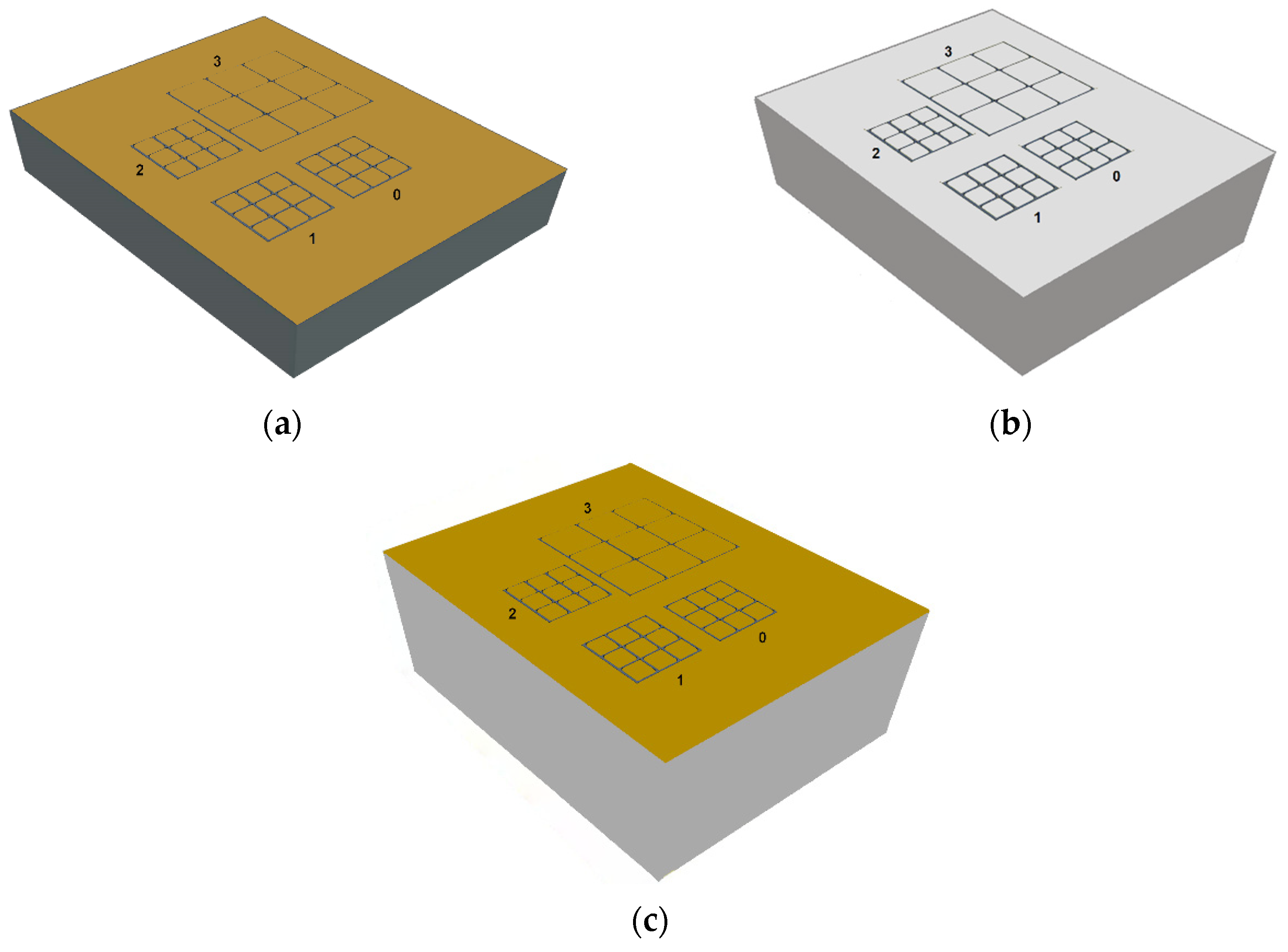
2.1. The CZT Pixel Detectors

The measurements involved CZT pixel detectors with quasi-ohmic electrical contacts (Au, Pt) characterized by different CZT crystals, with thicknesses between 1 and 3 mm. The 1-mm thick CZT detector was based on a boron oxide encapsulated vertical Bridgman (B-VB) CZT crystal, developed at IMEM-CNR of Parma with the collaboration of the due2lab company [32,33,34]. CZT detectors with gold electroless contacts are routinely fabricated at IMEM-CNR and are characterized by low leakage currents at room temperature (<1 nA cm−2 at 1000 V cm−1) [33,34,35]. In particular, 4% AuCl3 methanol solution was used for the cathode electrodes, while the anode patterns were obtained by photolithography and the passivation procedure was performed with an aqueous solution of H2O2 at 10% for 5 min. The thick detectors were based on travelling-heater-method THM-CZT crystals provided by Redlen Technologies (Saanichton, BC, Canada) [36,37,38,39]. In particular, besides the standard or low flux LF-THM CZT crystals (with enhanced electron charge transport properties), we also used high-flux HF-THM CZT crystals [40,41,42,43], recently fabricated by Redlen and characterized by enhanced hole charge transport properties to minimize high-flux radiation-induced polarization effects [44,45,46]. The details of the detectors (CZT crystals and electrical contacts) are better highlighted in Table 1. As shown in Figure 1, all detectors were characterized by four arrays of 3 × 3 pixels with pixel pitches of 500 µm and 250 µm and an inter-pixel gap of 50 µm; the cathode is a planar electrode covering the full crystal area.

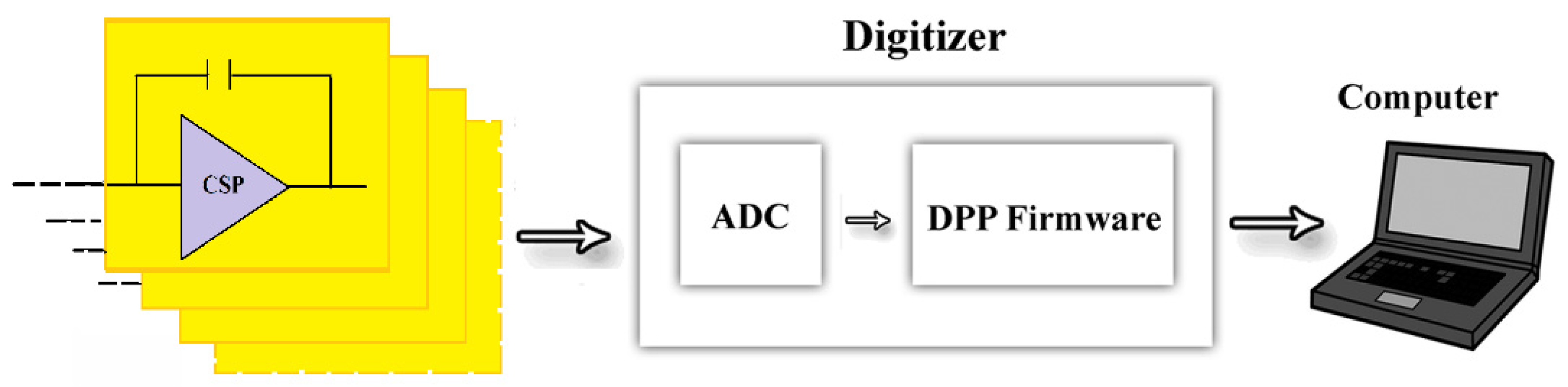
2.2. The Preamplifiers and the Digital Pulse Processing Electronics

Figure 2 shows a schematic view of the readout electronics used for all CZT pixel detectors.
The front-end electronics was represented by charge-sensitive preamplifiers (CSPs) without pulse shaping. They were based on a low-noise application specific integrated circuit (PIXIE ASIC) developed at the Rutherford Appleton Laboratory RAL (Didcot, UK) [47]. The PIXIE ASIC was equipped with 36 CSPs arranged in four arrays of 3 × 3 pads, flip-chip bonded directly to the pixels of the detectors (Figure 3).
Each array can be selected by the user providing, simultaneously, nine preamplifier outputs, with no pulse shaping processing. The electronic noise is very low, i.e., with an equivalent noise charge (ENC) less than 80 electrons. In this work, we only used the pixels of the 500-μm arrays.
The pulse shaping processing of the CSP output pulses was performed through a digital approach, using 16-channel digital electronics, developed at DiFC of the University of Palermo (Palermo, Italy) [48,49,50]. The digital electronics were based on commercial digitizers (DT5724, 16-bit, 100 MS/s, CAEN SpA, Italy; https://www.caen.it, accessed on 26 April 2022), where a dedicated firmware was uploaded [48,49,50]. The potentialities of the digital pulse processing approach are now widely recognized [51,52,53]; in our case, the flexibility of this approach, due to the possibility of using different pulse shaping features, was a key point for our investigation.
For each CSP output channel, the digital system performed on-line pulse detection, time-tag triggering, and pulse height analysis. The details of the pulse shaping operations and the outputs from each CSP output channel are described below:
(i)
Pulse detection and arrival time estimation; the CSP output waveforms were shaped using the classical single delay line (SDL) shaping technique [26], acting as the classical differentiation; the trigger time was generated and time-stamped through the ARC (amplitude and rise time compensation) timing marker (at the leading edge of the SDL pulses), able to reduce the distortions from time jitters and amplitude and rise time walks [26];
(ii)
Pulse height analysis (energy estimation); the detected CSP output pulses with the related arrival times were shaped with a classical trapezoidal filter [26]. We used trapezoidal-shaped pulses with peaking times (TS) ranging from 30 ns to 1000 ns.
Further details of the digital electronics are reported in our previous works [48,49,50].

2.3. Experimental Procedures

The measurements were performed at the laboratory of ionizing radiation detectors of the University of Palermo (Italy). All detectors were irradiated through the cathode electrode with uncollimated radiation sources (109Cd, 241Am and 57Co sources). High-flux measurements with X-ray tubes were conducted at the Livio Scarsi X-ray facility of the University of Palermo [54]. We used X-rays (main fluorescent lines at 17.5 and 19.6 keV) from a Mo target typical of mammographic X-ray beams. An overview of the experimental setup used is shown in Figure 4. All measurements were performed at room temperature (T = 20 °C).

3. Ballistic Deficit Pulse Processing in CZT Pixel Detectors: Measurements and Results

In this section, we will show the effects of the ballistic deficit pulse processing approach on the energy resolution, throughput, energy-linearity, time-stability, charge sharing, and pile-up in the CZT pixel detectors. A comparison with the results obtained from an energy resolution pulse processing, optimized for the best energy resolution, will be also presented.

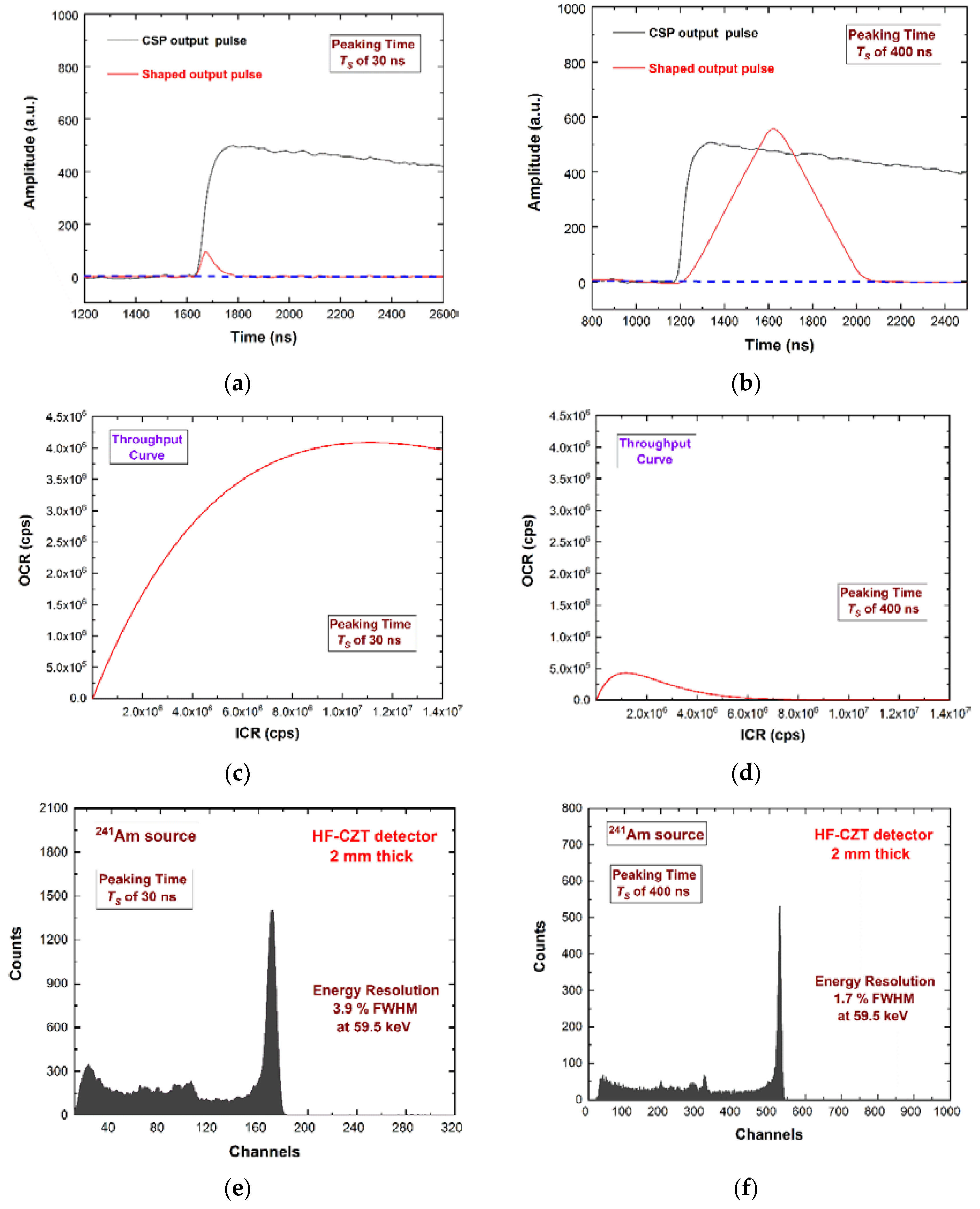
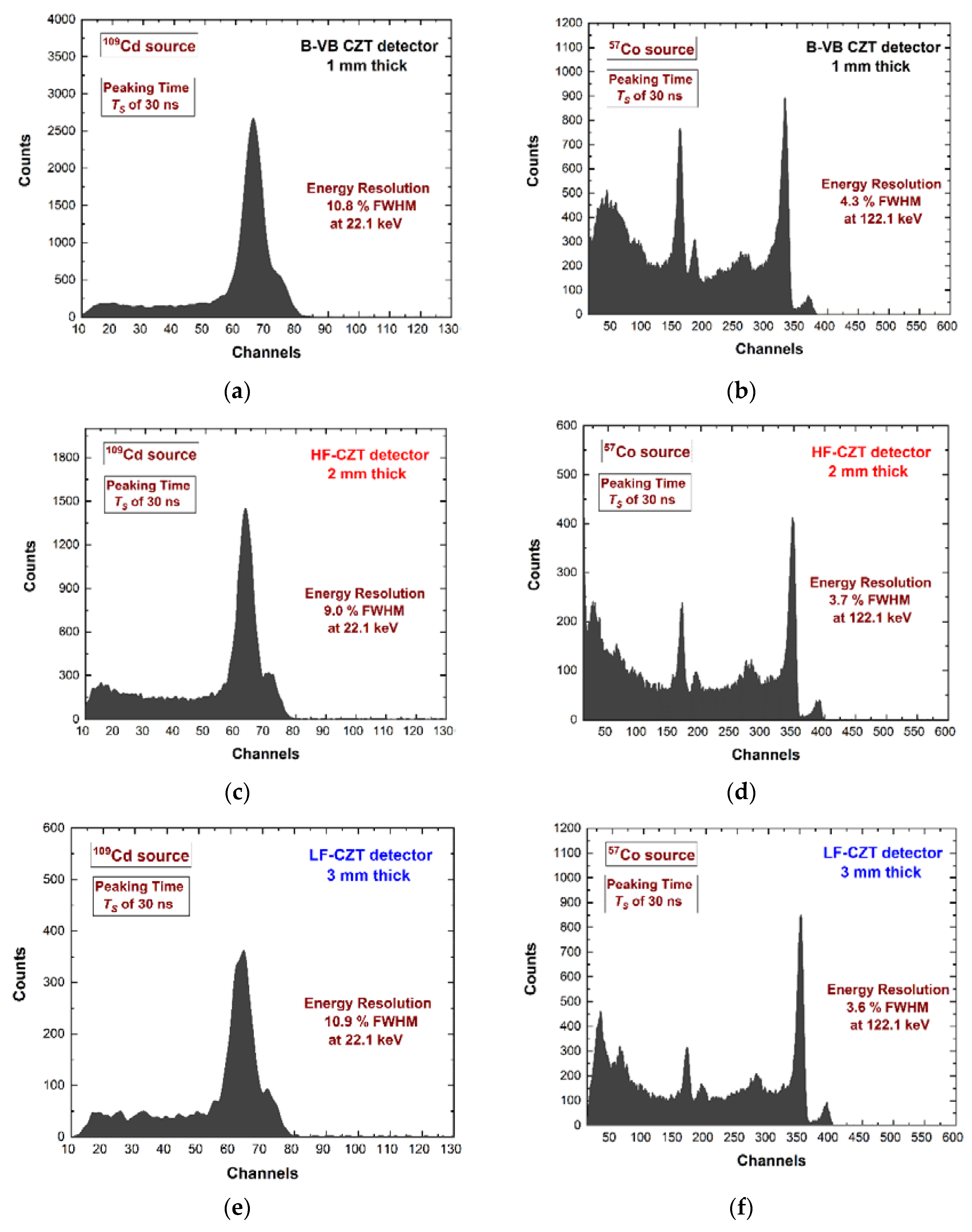
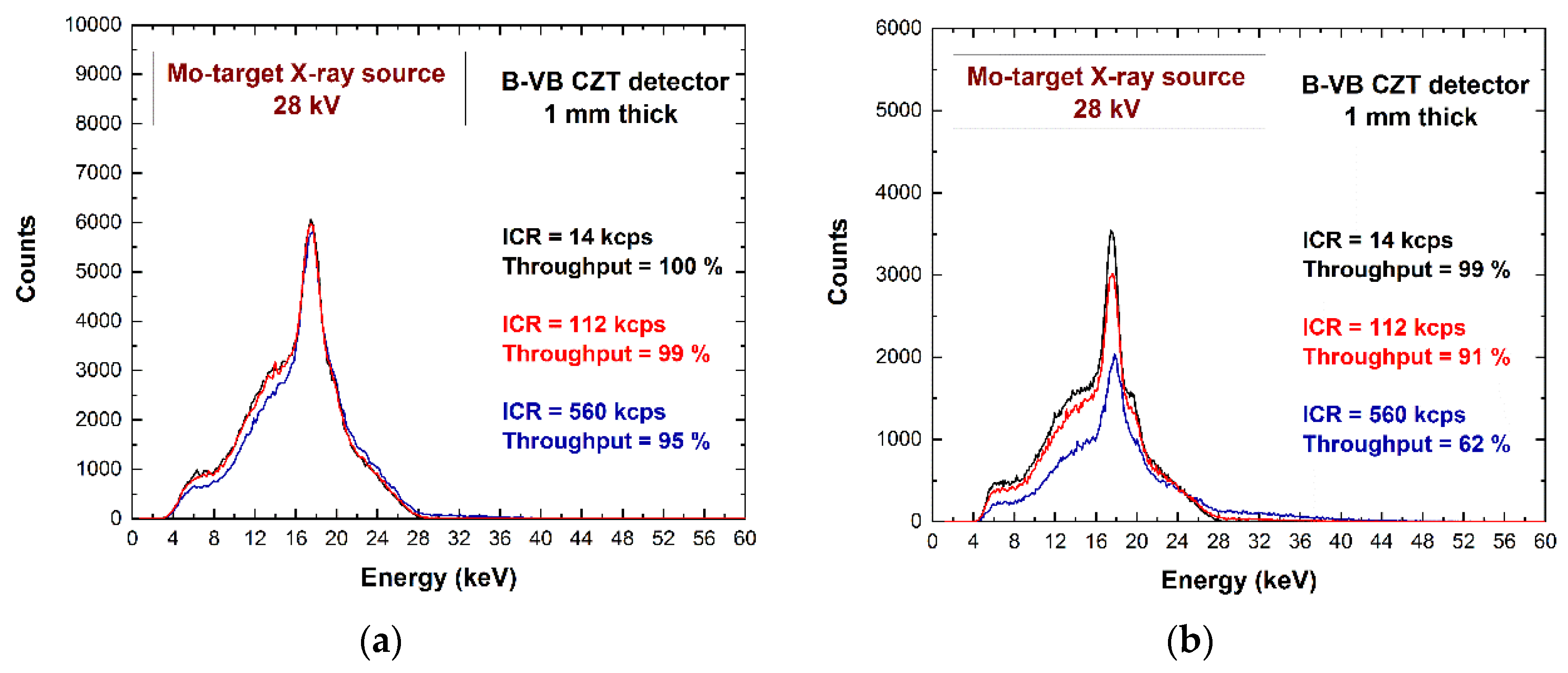
3.1. Energy Resolution and Throughput

The selection of the optimum shaping peaking time value (TS) is a key procedure for all radiation detectors [26]. Typically, the optimum TS value is chosen looking for the best energy resolution (energy resolution pulse processing). Figure 5 shows the energy resolution (FWHM) values at 59.5 keV measured at different TS values. All detectors were characterized by optimum TS values ranging from 300 ns to 400 ns; these values were always greater than the CSP peaking time TCSP (green dashed vertical lines), due to the minimization of the ballistic deficit fluctuations. As it is well-known in the literature [55], the optimum TS values also follow the equilibrium between two main electronic noise components. At high TS values, the parallel white noise (shot noise mainly due to the leakage current of the detectors) dominated the energy resolution, while at low TS values, the series white noise (thermal noise due to the drain current of preamplifier input FETs) was the main contributor. In our measurements, the degradation of the energy resolution at TS < TCSP was due to both the ballistic deficit and series noise effects.
In order to increase the throughput of the system (i.e., the ratio between the output and the input counting rate), the TS should be chosen as low as possible, taking into account the degradation of the energy resolution. In Figure 6, we present the performance of the 2-mm HF-CZT pixel detector, in terms of throughput and energy resolution (241Am source).
We used two different pulse shaping set-ups: the first with a TS of 30 ns selected for high throughput (ballistic deficit pulse processing), the second with a TS of 400 ns for the best energy resolution (energy resolution pulse processing). The mean value of the time widths of the shaped pulses over the detection threshold was 90 ns and 850 ns for TS of 30 ns and 400 ns, respectively. This time width was a dead time for the system and can be modelled as paralyzable dead time [26,56]. If a second pulse arrives while the first pulse is still above the detection threshold, the second pulse overlays the first, and extends the dead time by its width from its arrival time. Because the system counts threshold crossings, it will count only the first pulse. In agreement with the paralyzable dead time model, we calculated the throughput curves at the two-pulse processing set-up. The ballistic deficit pulse processing (dead time of 90 ns) ensured a maximum output counting rate (OCR) of 4.1 Mcps (Figure 6c), while the energy resolution pulse processing was of 0.43 Mcps (Figure 6d). Further energy spectra using the ballistic deficit pulse processing are shown in Figure 7.
Excellent energy resolution of 3.6% FWHM at 122 keV was obtained with the 3-mm CZT pixel detector. This was an interesting result when compared with the energy resolution of about 8% at 122 keV for the 3-mm CdTe pixel detectors using similar ballistic deficit pulse processing [29].

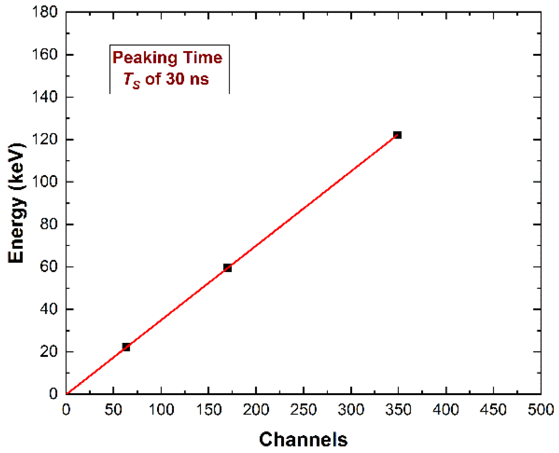
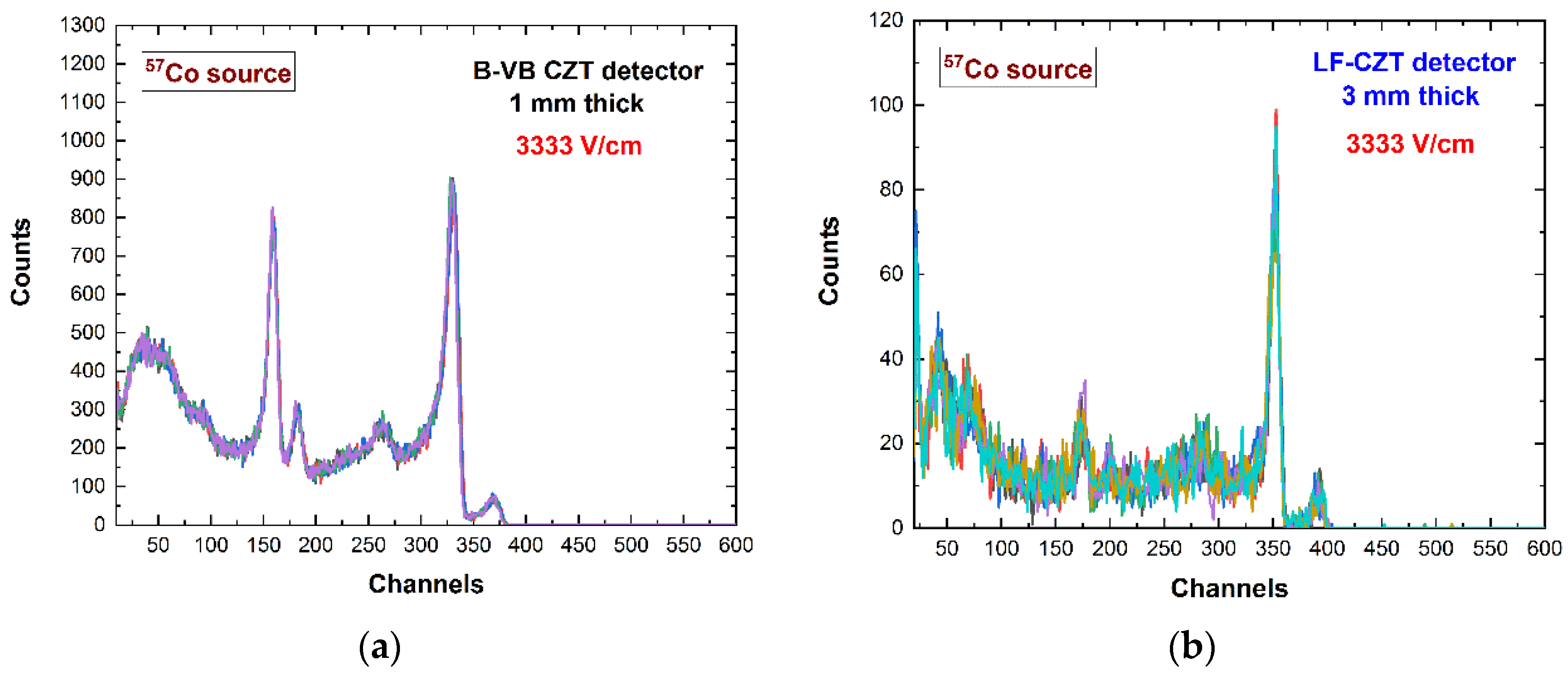
3.2. Energy Linearity and Time Stability
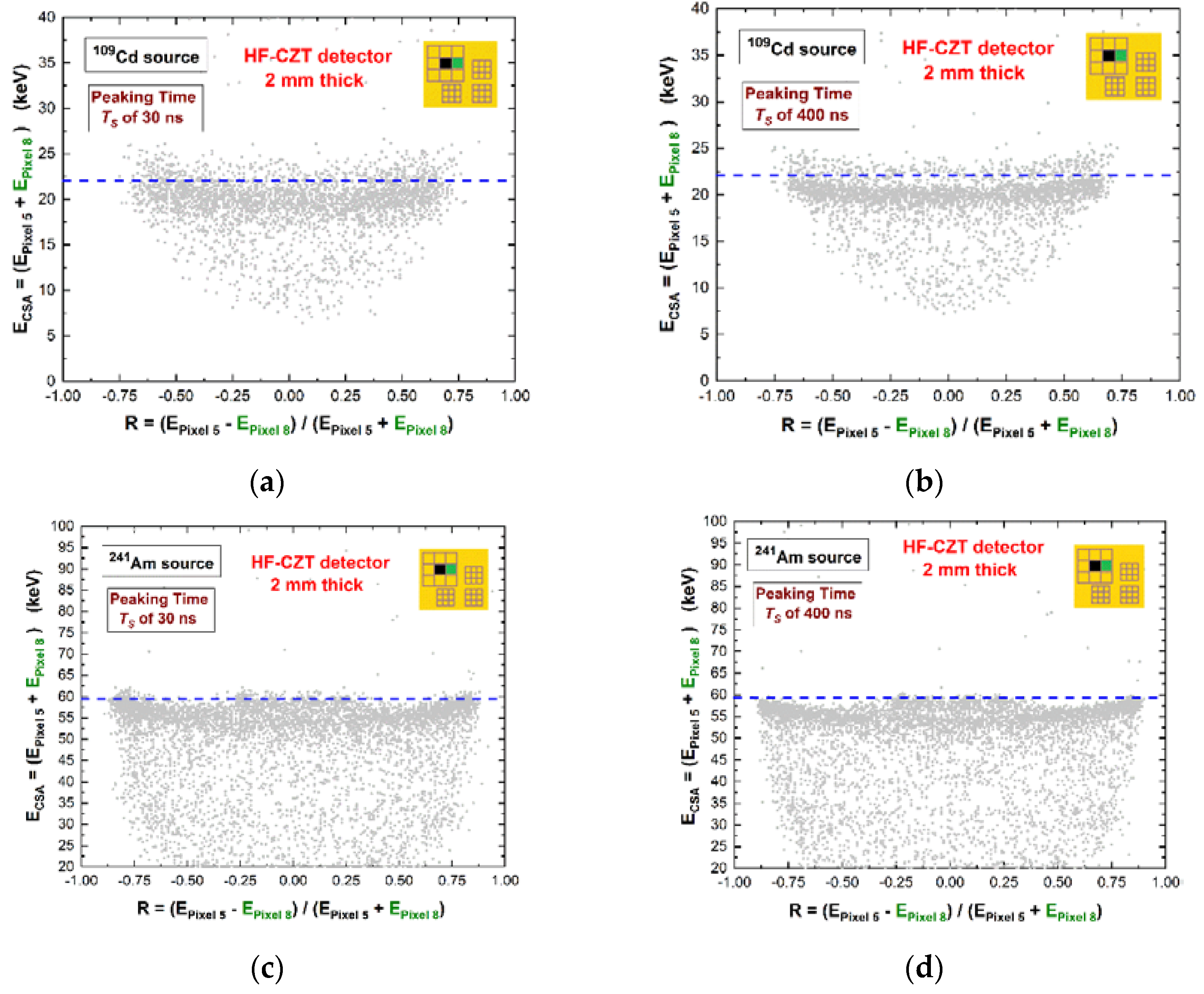
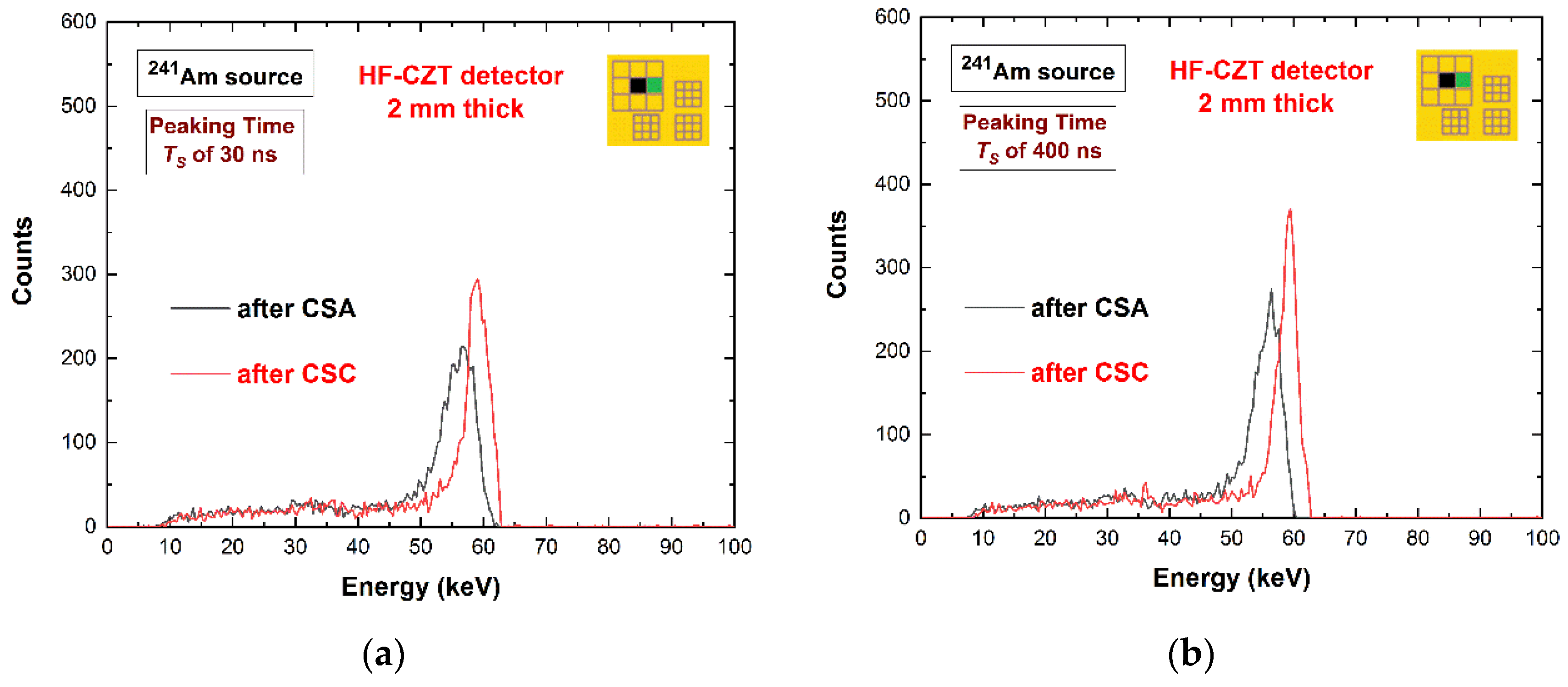
The linearity of the ballistic deficit pulse processing with energy was investigated. In particular, the linearity of the pulse heights with the photon energy was experimentally verified for all detectors, as shown in Figure 8.
As discussed in the introduction, CdTe detectors with quasi-ohmic electrical contacts, when working in ballistic deficit regimes, suffer from time instabilities due to the temporal changes of the electric field lines [29]. This was investigated in our detectors working at the same electric field set-up (3333 V/cm) used in CdTe detectors. In particular, Figure 9 shows the 57Co energy spectra measured within a time window of one hour. The time stability was well verified, demonstrating the more stable electrical contacts (Au, Pt) and electric field in quasi-ohmic CZT pixel detectors. This also highlighted the absence of temporal changes of the space charge in CZT materials.

3.3. Charge Sharing

The effects of the ballistic deficit pulse processing on the charge sharing measurements were also investigated. Typically, charge sharing is strongly present in sub-millimetre CZT pixel detectors. The percentage of charge sharing events is very high, of about 50–60% for the pixels with 500 μm pitches [23,48]. As it is well known, the energy of the shared events can be recovered by summing their energies, measured in temporal coincidence. However, the energy recovered after charge sharing addition (CSA) is often characterized by deficits, due to the presence of charge losses at the inter-pixel gap [57,58,59,60,61,62,63,64,65]. In our case, we investigated the effects of ballistic deficit pulse processing on these charge losses. Figure 10 shows the scatter plots of the summed energy ECSA versus the sharing ratio R. The energy ECSA = (EPixel5 + EPixel8) was the sum of the energies of two coincidence events between two adjacent pixels, i.e., after CSA, while the charge sharing ratio R was calculated from the ratio between the energy of the two coincidence events, as follows: R = (EPixel5 − EPixel8)/(EPixel5 + EPixel5). R is typically used to provide information about the interaction position of the shared events within the inter-pixel gap.
The plots on the left side were obtained using ballistic deficit pulse processing; on the right side, we used energy resolution pulse processing. Despite the poor energy distribution of the shared events (poor energy resolution), the ballistic deficit pulse processing did not increase the charge losses after CSA. This result is also shown in Figure 11, where the energy spectra after CSA (black lines) are presented. The charge losses (3 keV at 59.5 keV) were the same for both shaping processing approaches, even if the energy resolution of the energy spectra after CSA was poorer for the ballistic deficit pulse processing. Moreover, the correction of these charge losses was successfully performed for both processing approaches (red lines) through the application of a charge sharing correction (CSC) technique developed by our group and presented in our previous works [23,63]. The best energy resolution of the corrected energy spectra after CSC (red lines) was obtained with energy resolution pulse processing.

3.4. High Flux Performance

The goal of using ballistic deficit pulse processing was to obtain high throughput energy spectra with low pile-up effects and an energy resolution as high as possible. To investigate on the potentialities of this approach at high fluxes, we measured Mo-target X-ray spectra (with fluorescent X-ray lines at 17.5 keV and 19.6 keV) at different rates, up to a maximum saturation rate of the CSPs (600 kcps). The energy spectra, measured using both ballistic deficit and energy resolution pulse processing, are shown in Figure 12. At high rates (560 kcps), the ballistic deficit pulse processing gave the best results: similar energy resolution with the energy resolution pulse processing, high throughput (95%), and low pile-up effects in the spectra.
On the contrary, the effects of pile-up are visible when the energy resolution pulse processing was used, with the presence of more background events beyond the 28-keV end-point energy of the spectrum (blue line of Figure 12b).

4. Discussion

The measurements using the ballistic deficit pulse processing (shaped pulses with time widths of 90 ns) in CZT pixel detectors highlighted the following key results:
-
All detectors showed good energy resolutions of about 4% FWHM at 122 keV, in particular when compared with the energy resolution of about 8% obtained with 3-mm CdTe pixel detectors using similar ballistic deficit pulse processing [29]; this is due to the high bias voltage operation of the detectors (>5000 V/cm) which minimizes the changes of the charge collection times and, therefore, the effects of ballistic deficit; moreover, the series noise, very important in this shaping set-up, was also mitigated by the low noise front-end electronics (PIXIE ASICs).
-
The linearity of the pulse heights with the energy was verified in all CZT detectors.
-
We observed the absence of time instabilities, typically present in CdTe pixel detectors with quasi-ohmic electrical contacts [29]; this demonstrated the time stability of the electric field lines in the quasi-ohmic (Au, Pt) CZT detectors, highlighting the absence of space charge changes with time in CZT materials.
-
The ballistic deficit pulse processing did not increase the charge losses after the charge sharing addition (CSA) and the energy recovery was successfully applied.
-
At high rates (560 kcps), we measured energy spectra with very high throughput (95%), low pile-up effects, and a similar energy resolution obtained with the energy resolution pulse processing approach; potentially, the dead time of 90 ns, modelled as paralyzable dead time, can ensure a maximum output counting rate (OCR) of 4.1 Mcps.

5. Conclusions

In this work, we presented the potentialities of a ballistic deficit pulse processing approach for high-flux X-ray measurements with CZT pixel detectors. This approach consists of using shaped pulses with peaking times less than the peaking times of the preamplifier pulses. Despite the long peaking times of the preamplifiers (150–170 ns), we used digital shaped pulses with peaking times of 30 ns and a dead time less than 90 ns. Interesting energy resolution (4% at 122 keV) was obtained in various CZT pixel detectors, characterized by different thicknesses, crystals, and electrical contacts. The time instabilities, typically present in CdTe detectors, were not observed, demonstrating the absence of space charge changes with time in CZT materials.
Future activities will be focused on the use of new digitizers with a higher sampling frequency (>100 MHz) for performance enhancements in ballistic deficit pulse processing. We believe that the high sampling frequency can improve the pulse height analysis and the energy resolution of the detection systems.

Author Contributions

Conceptualization, L.A. and A.B.; formal analysis, L.A., A.B., G.G., F.P. and M.B.; investigation, L.A., A.B., F.P., M.C.V., P.S., S.Z., A.Z. and M.B.; writing—original draft preparation, A.B. and L.A.; writing—review and editing, all authors; supervision, L.A.; project administration, L.A.; funding acquisition, L.A. All authors have read and agreed to the published version of the manuscript.

Funding

This work was supported by the Italian Ministry for University and Research (MUR), under AVATAR X project No. POC01_00111 and by the European Union (EU) under the project—FESR o FSE, PON Ricerca e Innovazione 2014–2020—DM 1062/2021.

Acknowledgments

The authors would like to acknowledge the technical staff of the facility LAX at the University of Palermo, Marcello Mirabello, for his technical assistance during the high flux measurements.

Conflicts of Interest

The authors declare no conflict of interest.

References

  1. Barber, W.C.; Wessel, J.C.; Nygard, E.; Iwanczyk, J.S. Energy dispersive CdTe and CdZnTe detectors for spectral clinical CT and NDT applications. Nucl. Instr. Meth. A 2015, 784, 531–537. [Google Scholar] [CrossRef] [Green Version]
  2. Del Sordo, S.; Strazzeri, M.; Agnetta, G.; Biondo, B.; Celi, F.; Giarrusso, S.; Mangano, A.; Russo, F.; Caroli, E.; Donati, A.; et al. Spectroscopic performances of 16 × 16 pixel CZT imaging hard-X-ray detectors. Nuovo Cim. B 2004, 119, 257–270. [Google Scholar]
  3. Iwanczyk, J.; Nygard, E.; Meirav, O.; Arenson, J.; Barber, W.C.; Hartsough, N.E.; Malakhov, N.; Wessel, J.C. Photon Counting Energy Dispersive Detector Arrays for X-ray Imaging. IEEE Trans. Nucl. Sci. 2009, 56, 535–542. [Google Scholar] [CrossRef] [Green Version]
  4. Seller, P.; Bell, S.; Cernik, R.J.; Christodoulou, C.; Egan, C.K.; Gaskin, J.A.; Jacques, S.; Pani, S.; Ramsey, B.D.; Reid, C.; et al. Pixellated Cd(Zn)Te high-energy X-ray instrument. J. Inst. 2011, 6, C12009. [Google Scholar] [CrossRef]
  5. Szeles, C.; Soldner, S.A.; Vydrin, S.; Graves, J.; Bale, D.S. CdZnTe Semiconductor Detectors for Spectroscopic X-ray Imaging. IEEE Trans. Nucl. Sci. 2008, 55, 572–582. [Google Scholar] [CrossRef]
  6. Abbene, L.; Gerardi, G.; Principato, F. Digital performance improvements of a CdTe pixel detector for high flux energy-resolved X-ray imaging. Nucl. Instr. Meth. A 2015, 777, 54–62. [Google Scholar] [CrossRef]
  7. Iniewski, K. CZT detector technology for medical imaging. J. Inst. 2014, 9, C11001. [Google Scholar] [CrossRef]
  8. Nguyen, J.; Rodesch, P.A.; Richtsmeier, D.; Iniewski, K.; Bazalova-Carter, M. Optimization of a CZT photon counting detector for contaminant detection. J. Inst. 2021, 16, P11015. [Google Scholar] [CrossRef]
  9. Richtsmeier, D.; Guliyev, E.; Iniewski, K.; Bazalova-Carter, M. Contaminant detection in non-destructive testing using a CZT photon-counting detector. J. Inst. 2021, 16, P01011. [Google Scholar] [CrossRef]
  10. Del Sordo, S.; Abbene, L.; Caroli, E.; Mancini, A.M.; Zappettini, A.; Ubertini, P. Progress in the development of CdTe and CdZnTe semiconductor radiation detectors for astrophysical and medical applications. Sensors 2009, 9, 3491–3526. [Google Scholar] [CrossRef]
  11. Owens, A. Semiconductor materials and radiation detection. J. Synchrotron Rad. 2006, 13, 143–150. [Google Scholar] [CrossRef] [Green Version]
  12. Hernández-Gutiérrez, C.A.; Casallas-Moreno, Y.L.; Cardona, D.; Kudriavtsev, Y.; Santana-Rodríguez, G.; Mendoza-Pérez, R.; Contreras-Puente, G.; López-López, M.; Contreras-Puenteg, G.; Mendez-Garcia, V.H.; et al. Characterization of n-GaN/p-GaAs NP heterojunctions. Superlattices Microstruct. 2019, 136, 106298. [Google Scholar] [CrossRef]
  13. Reyes-Banda, M.G.; Regalado-Perez, E.; Pintor-Monroy, M.I.; Hernández-Gutiérrez, C.A.; Quevedo-López, M.A.; Mathew, X. Effect of Se diffusion and the role of a thin CdS buffer layer in the performance of a CdSe/CdTe solar cell. Superlattices Microstruct. 2019, 133, 106219. [Google Scholar] [CrossRef]
  14. Hernández-Gutiérrez, C.A.; Kudriavtsev, Y.; Mota, E.; Hernández, A.G.; Escobosa-Echavarría, A.; Sánchez-Resendiz, V.; Casallas-Moreno, Y.L.; López-López, M. A new method of making ohmic contacts to p-GaN. Nucl. Instr. Meth. B 2016, 388, 35–40. [Google Scholar] [CrossRef]
  15. Sammartini, M.; Gandola, M.; Mele, F.; Garavelli, B.; Macera, D.; Pozzi, P.; Bertuccio, G. X–γ -ray spectroscopy with a CdTe pixel detector and SIRIO preamplifier at deep sub microsecond signal-processing time. IEEE Trans. Nucl. Sci. 2021, 68, 70–75. [Google Scholar] [CrossRef]
  16. Sammartini, M.; Gandola, M.; Mele, F.; Garavelli, B.; Macera, D.; Pozzi, P.; Bertuccio, G. A CdTe pixel detector–CMOS preamplifier for room temperature high sensitivity and energy resolution X and γ ray spectroscopic imaging. Nucl. Instr. Meth. A 2018, 910, 168–173. [Google Scholar] [CrossRef]
  17. Wilson, M.D.; Bell, S.J.; Cernik, R.J.; Christodoulou, C.; Egan, C.K.; O’Flynn, D.; Jacques, S.; Veale, M.C.; Pani, S.; Scuffham, J.; et al. Multiple module pixellated CdTe spectroscopic X-ray detector. IEEE Trans. Nucl. Sci. 2013, 60, 1197–1200. [Google Scholar] [CrossRef]
  18. Meuris, A.; Limousin, O.; Lugiez, F.; Gevin, O.; Pinsard, F.; Le Mer, I.; Delagnes, E.; Vassal, M.C.; Soufflet, F.; Bocage, R. Caliste 64, an innovative CdTe hard X-ray micro-camera. IEEE Trans. Nucl. Sci. 2008, 55, 778–784. [Google Scholar] [CrossRef]
  19. Abbene, L.; Gerardi, G.; Turturici, A.A.; Del Sordo, S.; Principato, F. Experimental results from Al/p-CdTe/PtX-ray detectors. Nucl. Instr. Meth. A 2013, 730, 135–140. [Google Scholar] [CrossRef]
  20. Principato, F.; Turturici, A.A.; Gallo, M.; Abbene, L. Polarization phenomena in Al/p-CdTe/Pt X-ray detectors. Nucl. Instr. Meth. A 2013, 730, 141–145. [Google Scholar] [CrossRef]
  21. Principato, F.; Gerardi, G.; Abbene, L. Time-dependent current-voltage characteristics of Al/p-CdTe/Pt X-ray detectors. J. Appl. Phys. 2012, 112, 094506. [Google Scholar] [CrossRef]
  22. Farella, I.; Montagna, G.; Mancini, A.M.; Cola, A. Study on Instability Phenomena in CdTe Diode-Like Detectors. IEEE Trans. Nucl. Sci. 2009, 56, 1736–1742. [Google Scholar] [CrossRef]
  23. Abbene, L.; Gerardi, G.; Principato, F.; Bettelli, M.; Seller, P.; Veale, M.C.; Fox, O.; Sawhney, K.; Zambelli, N.; Benassi, G.; et al. Dual-polarity pulse processing and analysis for charge-loss correction in cadmium–zinc–telluride pixel detectors. J. Synchrotron Rad. 2018, 25, 1078–1092. [Google Scholar] [CrossRef] [PubMed]
  24. Buttacavoli, A.; Principato, F.; Gerardi, G.; Bettelli, M.; Sarzi Amadè, N.; Zappettini, A.; Seller, M.C.; Veale, O.; Fox, K.; Sawhney, K.; et al. Room-temperature performance of 3 mm-thick cadmium zinc telluride pixel detectors with sub-millimetre pixelization. J. Synchrotron Rad. 2020, 27, 1180–1189. [Google Scholar] [CrossRef] [PubMed]
  25. Gálvez, J.L.; Hernanz, M.; Álvarez, L.; Artigues, B.; Ullán, M.; Lozano, M.; Pellegrini, G.; Cabruja, E.; Martínez, R.; Chmeissani, M.; et al. Hard-X and gamma-ray imaging detector for astrophysics based on pixelated CdTe semiconductors. J. Inst. 2014, 11, C01011. [Google Scholar] [CrossRef]
  26. Knoll, G.F. (Ed.) Pulse shaping, counting, and timing. In Radiation Detection and Measurement, 4th ed.; John Wiley & Sons, Inc.: Hoboken, NJ, USA, 2010; pp. 649–650. [Google Scholar]
  27. Goulding, F.S.; Landis, D.A. Ballistic deficit correction in semiconductor detector spectrometers. IEEE Trans. Nucl. Sci. 1988, 35, 119–124. [Google Scholar] [CrossRef] [Green Version]
  28. Salathe, M.; Kihm, J.C. Optimized digital filtering techniques for radiation detection with HPGe detectors. Nucl. Instr. Meth. A 2016, 808, 150–155. [Google Scholar] [CrossRef] [Green Version]
  29. De Cesare, C.; Brambilla, A.; Ouvrier-Buffet, P.; Stanchina, S.; Rossetto, O.; Verger, L. An FPGA-based algorithm to correct the instability of high-resolution and high-flux X-ray spectroscopic imaging detectors. J. Inst. 2018, 13, P08022. [Google Scholar] [CrossRef]
  30. Brambilla, A.; Ouvrier-Buffet, P.; Gonon, G.; Rinkel, J.; Moulin, V.; Boudou, C.; Verger, L. Fast CdTe and CdZnTe semiconductor detector arrays for spectroscopic X-ray imaging. IEEE Trans. Nucl. Sci. 2013, 60, 408–415. [Google Scholar] [CrossRef]
  31. Brambilla, A.; Ouvrier-Buffet, P.; Rinkel, J.; Gonon, G.; Boudou, C.; Verger, L. CdTe linear pixel X-ray detector with enhanced spectrometric performance for high flux X-ray imaging. IEEE Trans. Nucl. Sci. 2012, 59, 1552–1558. [Google Scholar] [CrossRef]
  32. Abbene, L.; Principato, F.; Gerardi, G.; Buttacavoli, A.; Cascio, D.; Bettelli, M.; Amadè, N.S.; Seller, P.; Veale, M.C.; Fox, O.; et al. Room-Temperature X-ray response of cadmium-zinc-Telluride pixel detectors grown by the vertical Bridgman technique. J. Synchrotron Rad. 2020, 27, 319–328. [Google Scholar] [CrossRef] [PubMed] [Green Version]
  33. Abbene, L.; Gerardi, G.; Turturici, A.A.; Raso, G.; Benassi, G.; Bettelli, M.; Zambelli, N.; Zappettini, A.; Principato, F. X-ray response of CdZnTe detectors grown by the vertical Bridgman technique: Energy, temperature and high flux effects. Nucl. Instr. Meth. A 2016, 835, 1–12. [Google Scholar] [CrossRef]
  34. Benassi, G.; Nasi, L.; Bettelli, M.; Zambelli, N.; Calestani, D.; Zappettini, A. Strong mechanical adhesion of gold electroless contacts on CdZnTe deposited by alcoholic solutions. J. Inst. 2017, 12, P02018. [Google Scholar] [CrossRef]
  35. Auricchio, N.; Marchini, L.; Caroli, E.; Zappettini, A.; Abbene, L.; Honkimaki, V. Charge transport properties in CdZnTe detectors grown by the vertical Bridgman technique. J. Appl. Phys. 2011, 110, 124502. [Google Scholar] [CrossRef]
  36. Abbene, L.; Gerardi, G.; Raso, G.; Principato, F.; Zambelli, N.; Benassi, G.; Bettelli, M.; Zappettini, A. Development of new CdZnTe detectors for room-temperature high-flux radiation measurements. J. Synchrotron Rad. 2017, 24, 429–438. [Google Scholar] [CrossRef]
  37. Iniewski, K. CZT sensors for Computed Tomography: From crystal growth to image quality. J. Inst. 2016, 11, C12034. [Google Scholar] [CrossRef]
  38. Chen, H.; Awadalla, S.A.; Iniewski, K.; Lu, P.H.; Harris, F.; MacKenzie, J.; Hasanen, T.; Chen, W.; Redden, R.; Bindley, G.; et al. Characterization of large cadmium zinc telluride crystals grown by traveling heater method. J. Appl. Phys. 2008, 103, 014903. [Google Scholar] [CrossRef] [Green Version]
  39. Chen, H.; Awadalla, S.A.; Mackenzie, J.; Redden, R.; Bindley, G.; Bolotnikov, A.E.; Camarda, G.S.; Carini, G.; James, R.B. Characterization of Traveling Heater Method (THM) Grown Cd0.9Zn0.1Te Crystals. IEEE Trans. Nucl. Sci. 2007, 54, 811–816. [Google Scholar] [CrossRef]
  40. Thomas, B.; Veale, M.C.; Wilson, M.D.; Seller, P.; Schneider, A.; Iniewski, K. Characterisation of Redlen high-flux CdZnTe. J. Inst. 2017, 12, C12045. [Google Scholar] [CrossRef]
  41. Veale, M.C.; Booker, P.; Cross, S.; Hart, M.D.; Jowitt, L.; Lipp, J.; Schneider, A.; Seller, P.; Wheater, R.M.; Wilson, M.D.; et al. Characterization of the Uniformity of High-Flux CdZnTe Material. Sensors 2020, 20, 2747. [Google Scholar] [CrossRef]
  42. Koch-Mehrin, K.A.L.; Bugby, S.L.; Lees, J.E.; Veale, M.C.; Wilson, M.D. Charge Sharing and Charge Loss in High-Flux Capable Pixelated CdZnTe Detectors. Sensors 2021, 21, 3260. [Google Scholar] [CrossRef] [PubMed]
  43. Buttacavoli, A.; Principato, F.; Gerardi, G.; Cascio, D.; Raso, G.; Bettelli, M.; Zappettini, A.; Seller, P.; Veale, M.C.; Abbene, L. Incomplete Charge Collection at Inter-Pixel Gap in Low-and High-Flux Cadmium Zinc Telluride Pixel Detectors. Sensors 2022, 22, 1441. [Google Scholar] [CrossRef] [PubMed]
  44. Wang, X.; Xiao, S.; Li, M.; Zhang, L.; Cao, Y.; Chen, Y. Further process of polarization within a pixellated CdZnTe detector under intense X-ray irradiation. Nucl. Instr. Meth. A 2013, 700, 75–80. [Google Scholar] [CrossRef]
  45. Sellin, P.J.; Prekas, G.; Franc, J.; Grill, R. Electric field distributions in CdZnTe due to reduced temperature and X-ray irradiation. Appl. Phys. Let. A 2010, 96, 133509. [Google Scholar] [CrossRef] [Green Version]
  46. Bale, D.S.; Szeles, C. Nature of polarization in wide-bandgap semiconductor detectors under high-flux irradiation: Application to semi-insulating Cd1−xZnxTe. Phys. Rev. B 2008, 77, 035205. [Google Scholar] [CrossRef] [Green Version]
  47. Veale, M.C.; Bell, S.J.; Jones, L.L.; Seller, P.; Wilson, M.D.; Allwork, C.; Cernik, R.C. An ASIC for the study of charge sharing effects in small pixel CdZnTe X-ray detectors. IEEE Trans. Nucl. Sci. 2011, 58, 2357–2362. [Google Scholar] [CrossRef]
  48. Abbene, L.; Principato, F.; Gerardi, G.; Bettelli, M.; Seller, P.; Veale, M.C.; Zappettini, A. Digital fast pulse shape and height analysis on cadmium–zinc–telluride arrays for high-flux energy-resolved X-ray imaging. J. Synchrotron Rad. 2018, 25, 257–271. [Google Scholar] [CrossRef]
  49. Abbene, L.; Gerardi, G.; Raso, G.; Basile, S.; Brai, M.; Principato, F. Energy resolution and throughput of a new real time digital pulse processing system for X-ray and gamma ray semiconductor detectors. J. Inst. 2013, 8, P07019. [Google Scholar] [CrossRef]
  50. Gerardi, G.; Abbene, L. A digital approach for real time high-rate high-resolution radiation measurements. Nucl. Instr. Meth. A 2014, 768, 46–54. [Google Scholar] [CrossRef] [Green Version]
  51. Dambacher, M.; Zwerger, A.; Fauler, A.; Disch, C.; Stohlker, U.; Fiederle, M. Development of the gamma-ray analysis digital filter multi-channel analyzer (GMCA). Nucl. Instr. Meth. A 2011, 652, 445–449. [Google Scholar] [CrossRef]
  52. Jordanov, V.T.; Knoll, G.F.; Huber, A.C.; Pantazis, J.A. Digital techniques for real-time pulse shaping in radiation measurements. Nucl. Instr. Meth. A 1994, 353, 261–264. [Google Scholar] [CrossRef] [Green Version]
  53. Abbene, L.; Gerardi, G.; Principato, F.; Del Sordo, S.; Raso, G. Direct measurement of mammographic X-ray spectra with a digital CdTe detection system. Sensors 2012, 12, 8390–8404. [Google Scholar] [CrossRef] [PubMed]
  54. Principato, F.; Gerardi, G.; Turturici, A.A.; Raso, G.; Quartararo, M.; Pintacuda, F.; Abbene, L. The “livio scarsi” X-ray facility at university of palermo for device testing. In Proceedings of the European Conference on Radiation and its Effects on Components and Systems, RADECS, Moscow, Russia, 14–18 September 2015; p. 7365672. [Google Scholar]
  55. Bertuccio, G.; Pullia, A.; De Geronimo, G. Criteria of choice of the front-end transistor for low-noise preamplification of detector signals at sub-microsecond shaping times for X- and γ-ray spectroscopy. Nucl. Instr. Meth. A 1996, 380, 301–307. [Google Scholar] [CrossRef]
  56. Abbene, L.; Gerardi, G. High-rate dead-time corrections in a general purpose digital pulse processing system. J. Synchrotron Rad. 2015, 22, 1190–1201. [Google Scholar] [CrossRef] [PubMed]
  57. Lai, X.; Shirono, J.; Araki, H.; Budden, B.; Cai, L.; Kawata, G.; Thompson, R. Modeling Photon Counting Detector Anode Street Impact on Detector Energy Response. IEEE Trans. Rad. Plas. Med. Sci. 2020, 5, 476–484. [Google Scholar] [CrossRef]
  58. Kim, J.K.; Anderson, S.E.; Kaye, W.; Zhang, F.; Zhu, Y.; Kaye, S.J.; He, Z. Charge sharing in common-grid pixelated CdZnTe detectors. Nucl. Instr. Meth. A 2011, 654, 233–243. [Google Scholar] [CrossRef]
  59. Bugby, S.L.; Koch-Mehrin, K.A.L.; Veale, M.C.; Wilson, M.D.; Lees, J.E. Energy-loss correction in charge sharing events for improved performance of pixellated compound semiconductors. Nucl. Instr. Meth. A 2019, 940, 142–151. [Google Scholar] [CrossRef]
  60. Kalemci, E.; Matteson, J.L. Investigation of charge sharing among electrode strips for a CdZnTe detector. Nucl. Instr. Meth. A 2002, 478, 527–537. [Google Scholar] [CrossRef] [Green Version]
  61. Gaskin, J.A.; Sharma, D.P.; Ramsey, B.D. Charge sharing and charge loss in a cadmium–zinc–telluride fine-pixel detector array. Nucl. Instr. Meth. A 2003, 505, 122–125. [Google Scholar] [CrossRef]
  62. Bolotnikov, A.E.; Cook, W.R.; Harrison, F.A.; Wong, A.S.; Schindler, S.M.; Eichelberger, A.C. Charge loss between contacts of CdZnTe pixel detectors. Nucl. Instr. Meth. A 1999, 432, 326–331. [Google Scholar] [CrossRef]
  63. Buttacavoli, A.; Gerardi, G.; Principato, F.; Mirabello, M.; Cascio, D.; Raso, G.; Bettelli, M.; Zappettini, A.; Seller, P.; Veale, M.C.; et al. Energy recovery of multiple charge sharing events in room temperature semiconductor pixel detectors. Sensors 2021, 21, 3669. [Google Scholar] [CrossRef] [PubMed]
  64. Pickford Scienti, O.L.P.; Bamber, J.C.; Darambara, D.G. Cdte based energy resolving, X-ray photon counting detector performance assessment: The effects of charge sharing correction algorithm choice. Sensors 2020, 20, 6093. [Google Scholar] [CrossRef] [PubMed]
  65. Vasylchenko, I.; Grill, R.; Belas, E.; Praus, P.; Musiienko, A. Charge sharing in (CdZn)te pixel detector characterized by laser-induced transient currents. Sensors 2020, 20, 85. [Google Scholar] [CrossRef] [PubMed] [Green Version]
Figure 1. The anode layout of the three CZT pixel detectors. (a) The 1-mm thick B-VB CZT pixel detector, (b) the 2-mm thick HF-CZT pixel detector, and (c) the 3-mm LF-CZT pixel detector. The different colours highlight the related differences in both the CZT crystals and electrical contacts.
Sensors 22 03409 g001
Figure 2. Schematic view of the readout electronic circuit architecture. On the left, there is the charge-sensitive preamplifiers of the PIXIE ASIC [47], where the CZT pixels were flip-chip bonded; the pulse shaping and the pulse height analysis was performed by custom digital pulse processing electronics [48,49,50] controlled through a PC.
Sensors 22 03409 g002
Figure 3. The 3-mm LF-CZT pixel detector flip-chip bonded on the PIXIE ASIC. A bias voltage of −1800 V was supplied by a gold wire glued on the planar cathode electrode, clearly visible in the picture.
Sensors 22 03409 g003
Figure 4. An overview of the experimental setup used for high-flux X-ray measurements at the Livio Scarsi X-ray facility. The CZT pixel detectors (enclosed in the grey rectangular box, together with the preamplifier PIXIE ASIC) were irradiated with Mo target X-rays (the tube on the right side). The red boxes, on the bottom right side, are the digitizers of the digital pulse processing electronics. The detector box was mounted on a micro-translator system, which can be moved in x, y, and z directions with a precision of 10 μm.
Sensors 22 03409 g004
Figure 5. Measurement of the energy resolution (FWHM) at 59.5 keV vs. the peaking time of the shaped pulses. The results for the (a) B-VB CZT pixel detector, (b) HF-CZT pixel detector, and (c) LF-CZT pixel detector. The green dashed vertical lines represent the mean value of the peaking times TCSP of the CSP output pulses.
Sensors 22 03409 g005
Figure 6. The preamplifier output pulses (black lines) and the shaped output pulses (red lines) with peaking times TS of (a) 30 ns (ballistic deficit pulse processing) and (b) 400 ns (energy resolution pulse processing). The calculated throughput curves, i.e., the output counting rate (OCR) vs. the input counting rate (ICR), with TS of (c) 30 ns and (d) 400 ns. The throughput curves were calculated considering paralyzable dead times (the full-time width of the shaped pulses over the threshold) of 90 ns and 850 ns for TS = 30 ns and 400 ns, respectively. The measured 241Am energy spectra with TS equal to (e) 30 ns and (f) 400 ns. To optimize the binning of the pulse heights of the shaped pulses at TS of 30 ns, we used an amplitude gain equal to 2.
Sensors 22 03409 g006
Figure 7. Measured (a,c,e) 109Cd and (b,d,f) 57Co energy spectra for the three CZT pixel detectors. All spectra were obtained using the ballistic deficit pulse processing with a peaking time TS of 30 ns (dead time of 90 ns).
Sensors 22 03409 g007
Figure 8. The photon energy vs. the pulse height (channels) obtained using the ballistic deficit pulse processing approach. The linearity with energy was well verified.
Sensors 22 03409 g008
Figure 9. The energy spectra measured with the (a) B-VB CZT pixel detector and (b) LF-CZT pixel detector within a time window of one hour. For each time window of one hour, we measured six energy spectra with an acquisition time of ten minutes. 57Co sources with different activity were used. The time stability was verified.
Sensors 22 03409 g009
Figure 10. Two-dimensional (2D) scatter plot of the summed energy of the coincidence events (multiplicity m = 2) between pixel no. 5 and pixel no. 8 after, the charge sharing addition (CSA), versus the sharing ratio R. (a,c) Ballistic deficit pulse processing; (b,d) energy resolution pulse processing. The blue dashed lines represent the true energy.
Sensors 22 03409 g010
Figure 11. The energy spectra after CSA (black line) and after CSC (red line). (a) Ballistic deficit pulse processing; (b) energy resolution pulse processing.
Sensors 22 03409 g011
Figure 12. The Mo-target X-ray spectra at different input counting rates (ICRs). (a) Ballistic deficit pulse processing; (b) energy resolution pulse processing.
Sensors 22 03409 g012
Table 1. The key characteristics of the CZT pixel detectors.
CZT CrystalsMobility-Lifetime
Products
μτ (cm2/V)
Electrical Contacts
B-VB CZT
(4.25 × 3.25 × 1 mm3)
IMEM-CNR Parma (Parma, Italy) 1
due2lab s.r.l. (Scandiano, Italy) 1
μeτe 0.6–0.7 × 10⁻³
μhτh not measured
gold (Au) electroless quasi-ohmic
IMEM-CNR Parma (Italy) 1
due2lab s.r.l. (Italy) 1
HF-CZT
(4.25 × 3.25 × 2 mm3)
Redlen Technologies
(Canada) 1
μeτe 2–3 × 10⁻³
μhτh 1–2 × 10⁻⁴
platinum (Pt) quasi-ohmic
Redlen Technologies
(Canada) 1
LF-CZT
(4.25 × 3.25 × 3 mm3)
Redlen Technologies
(Canada) 1
μeτe 1–3 × 10⁻²
μhτh 2–3 × 10⁻⁵
gold (Au) electroless quasi-ohmic
IMEM-CNR Parma (Italy) 1
due2lab s.r.l. (Italy) 1
1 The manufacturers.
Publisher’s Note: MDPI stays neutral with regard to jurisdictional claims in published maps and institutional affiliations.

