
High Sensitivity Surface Plasmon Resonance Sensor Based on a Ge-Doped Defect and D-Shaped Microstructured Optical Fiber


Abstract
:1. Introduction
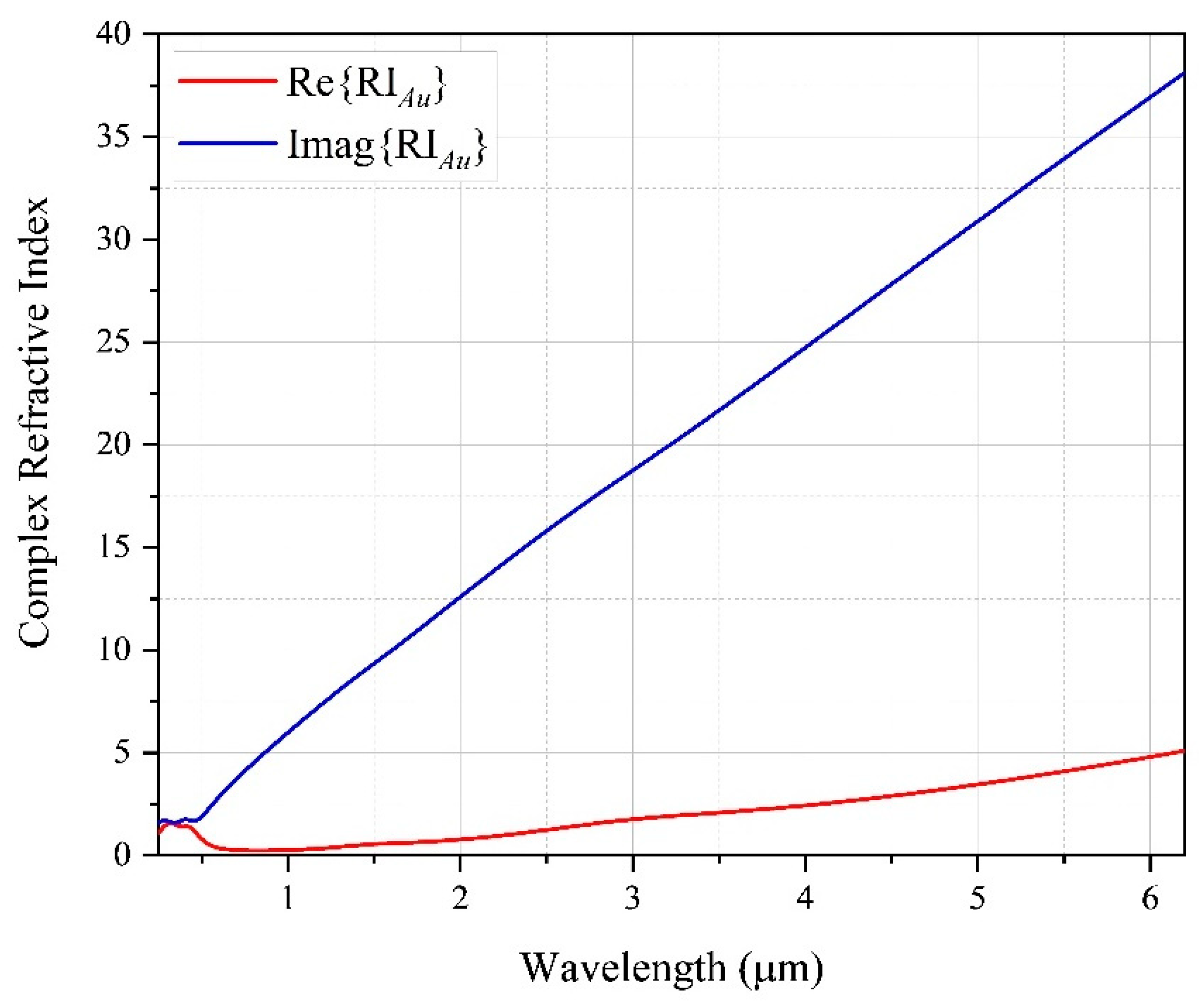
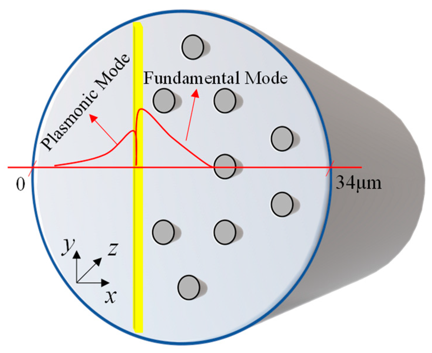
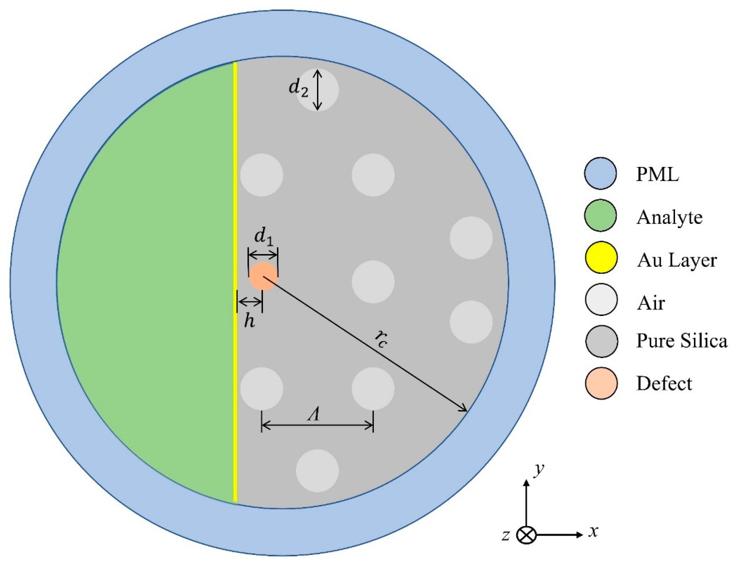
2. Plasmonic Sensor Design and Simulation
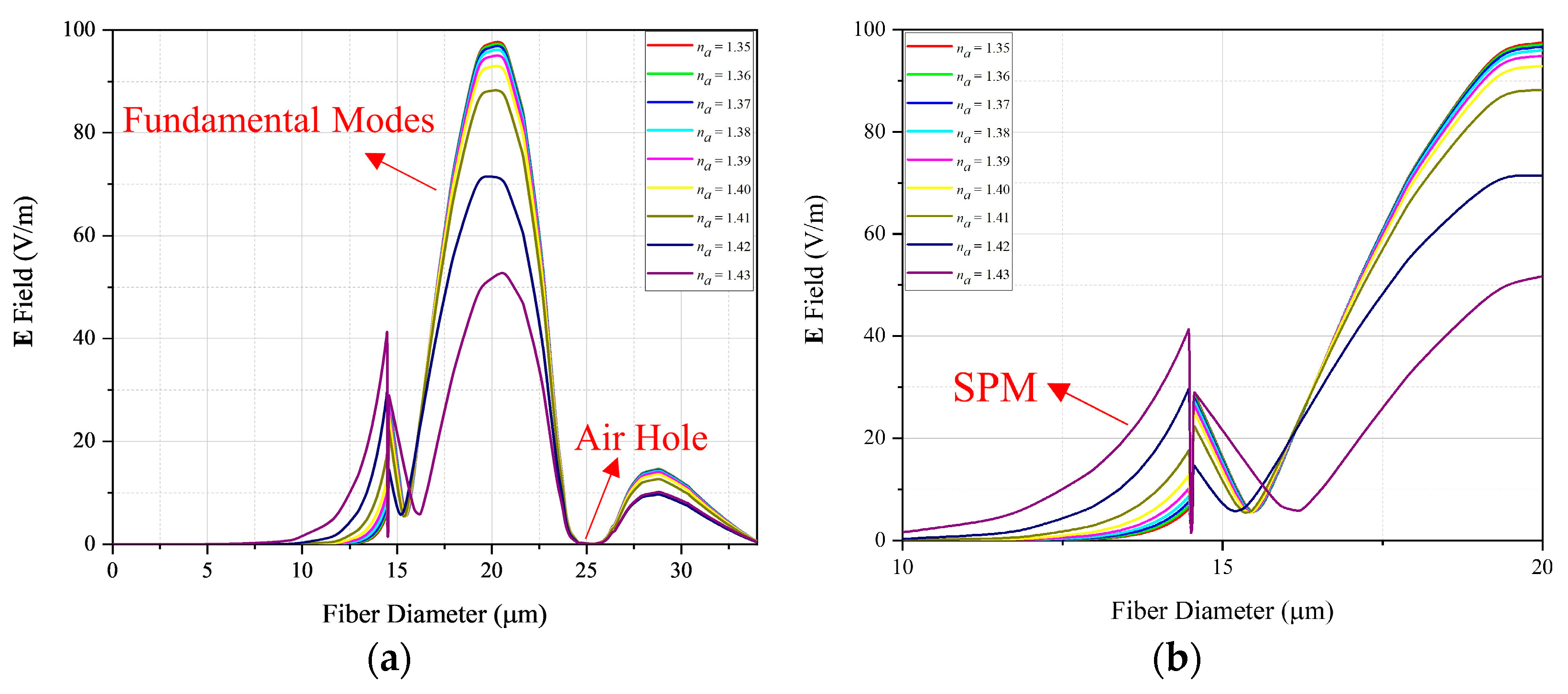
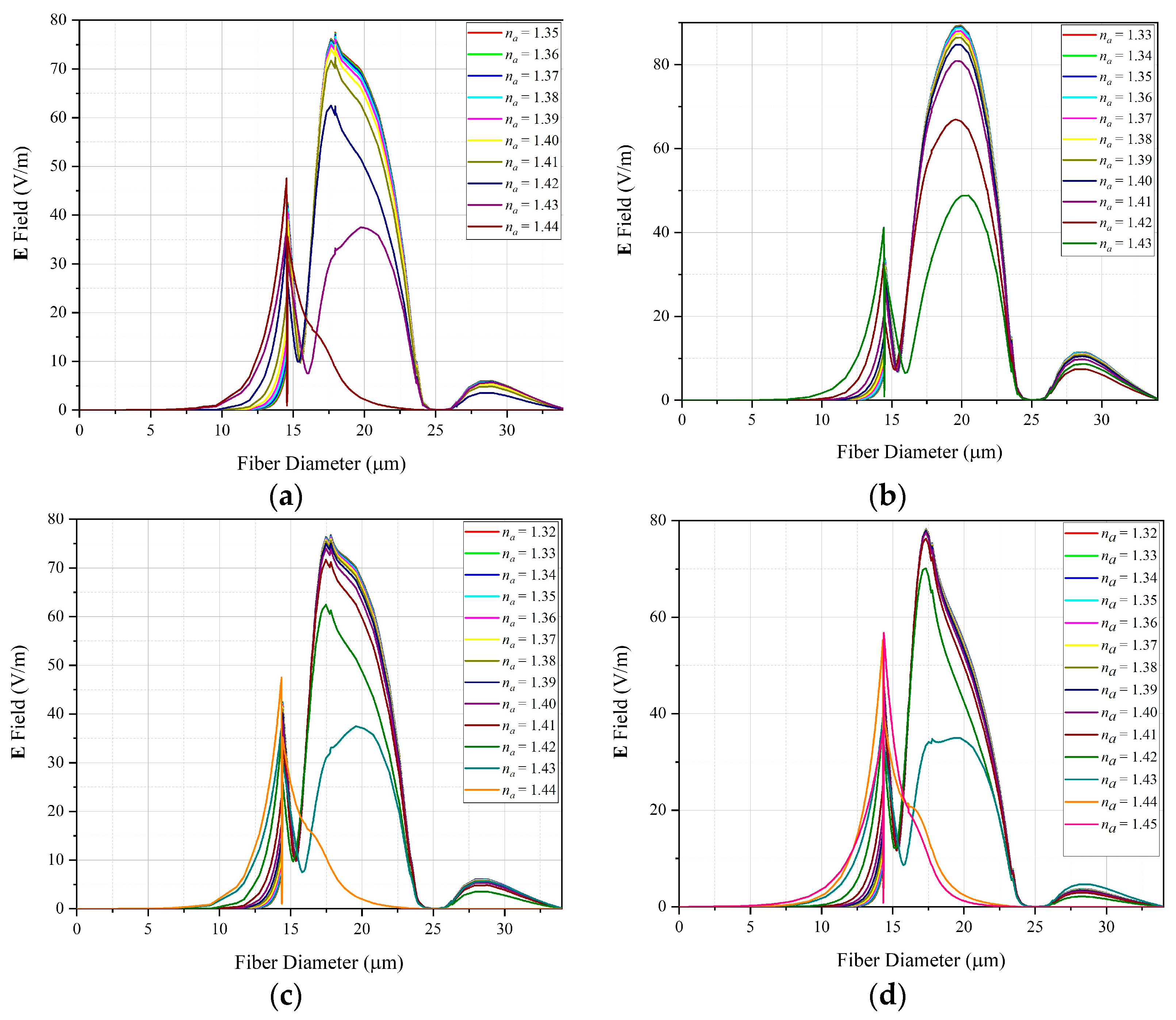
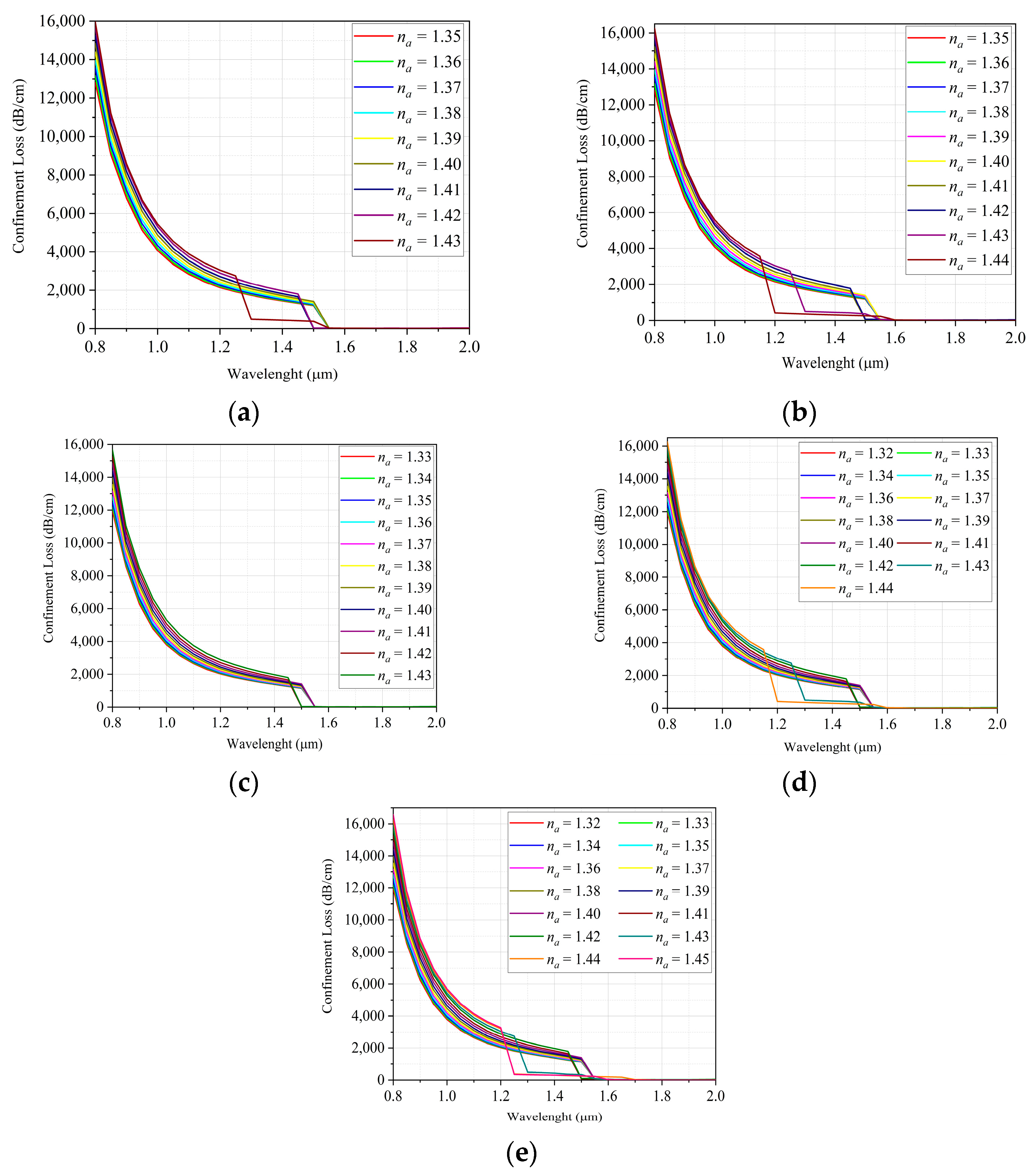
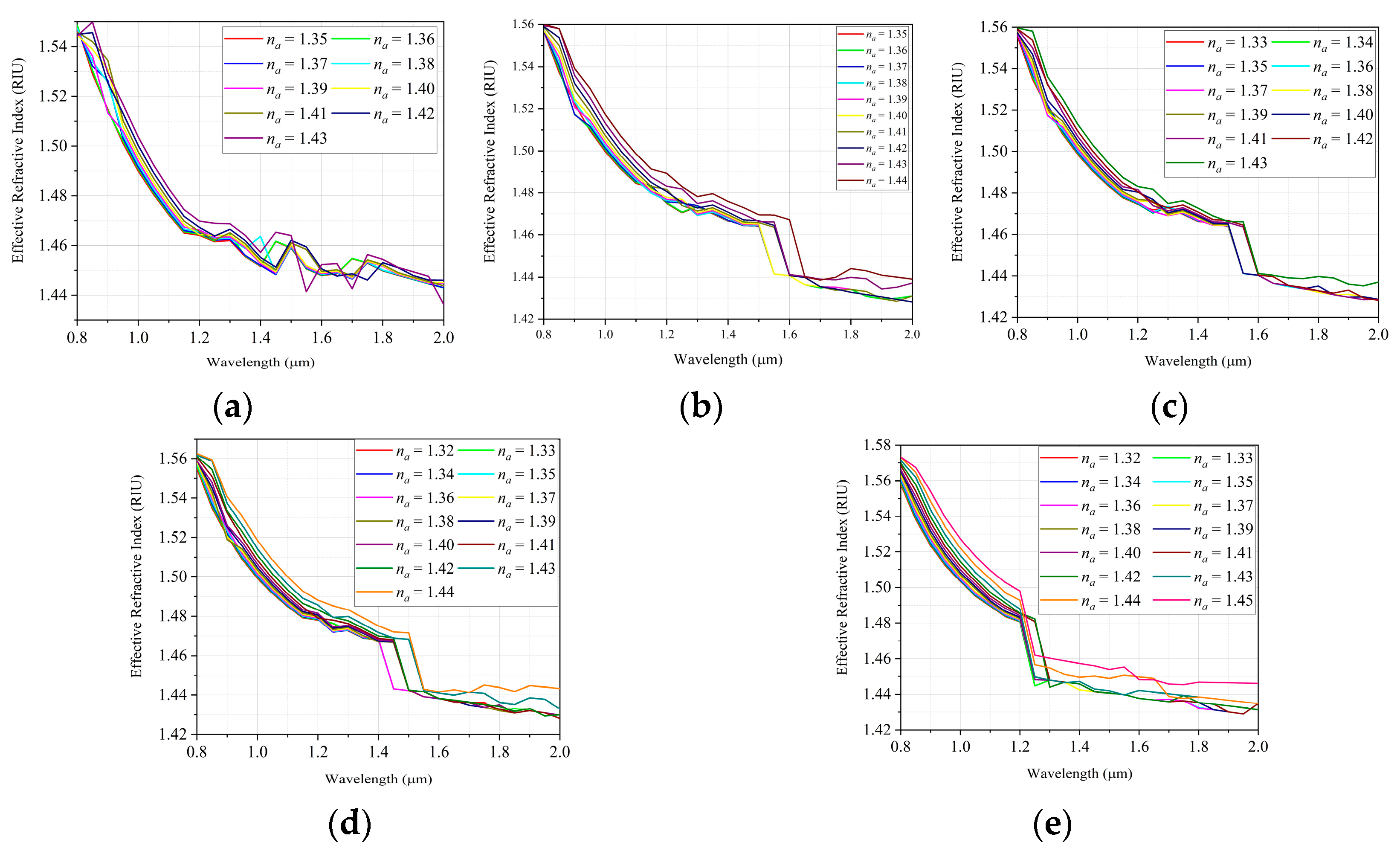
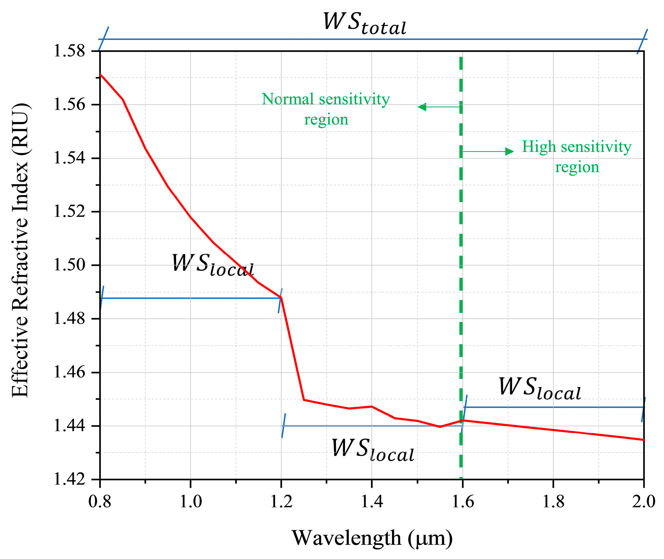
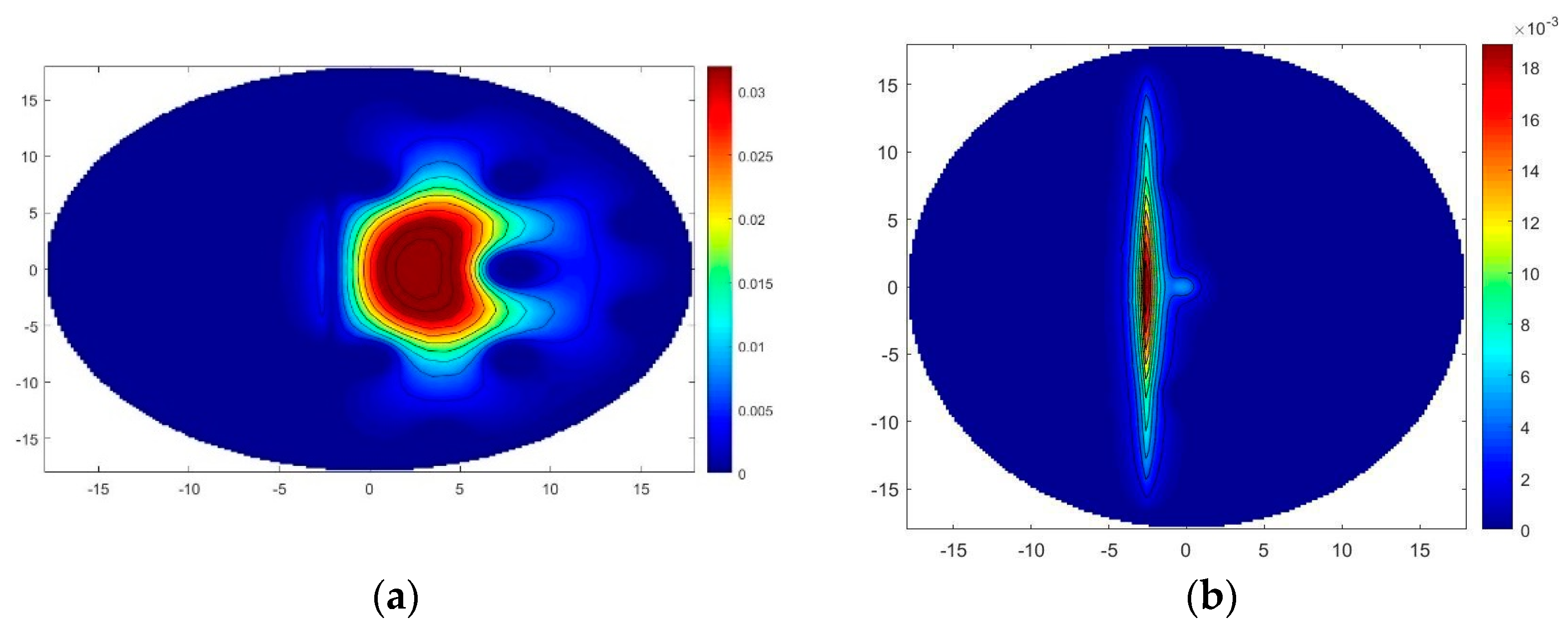
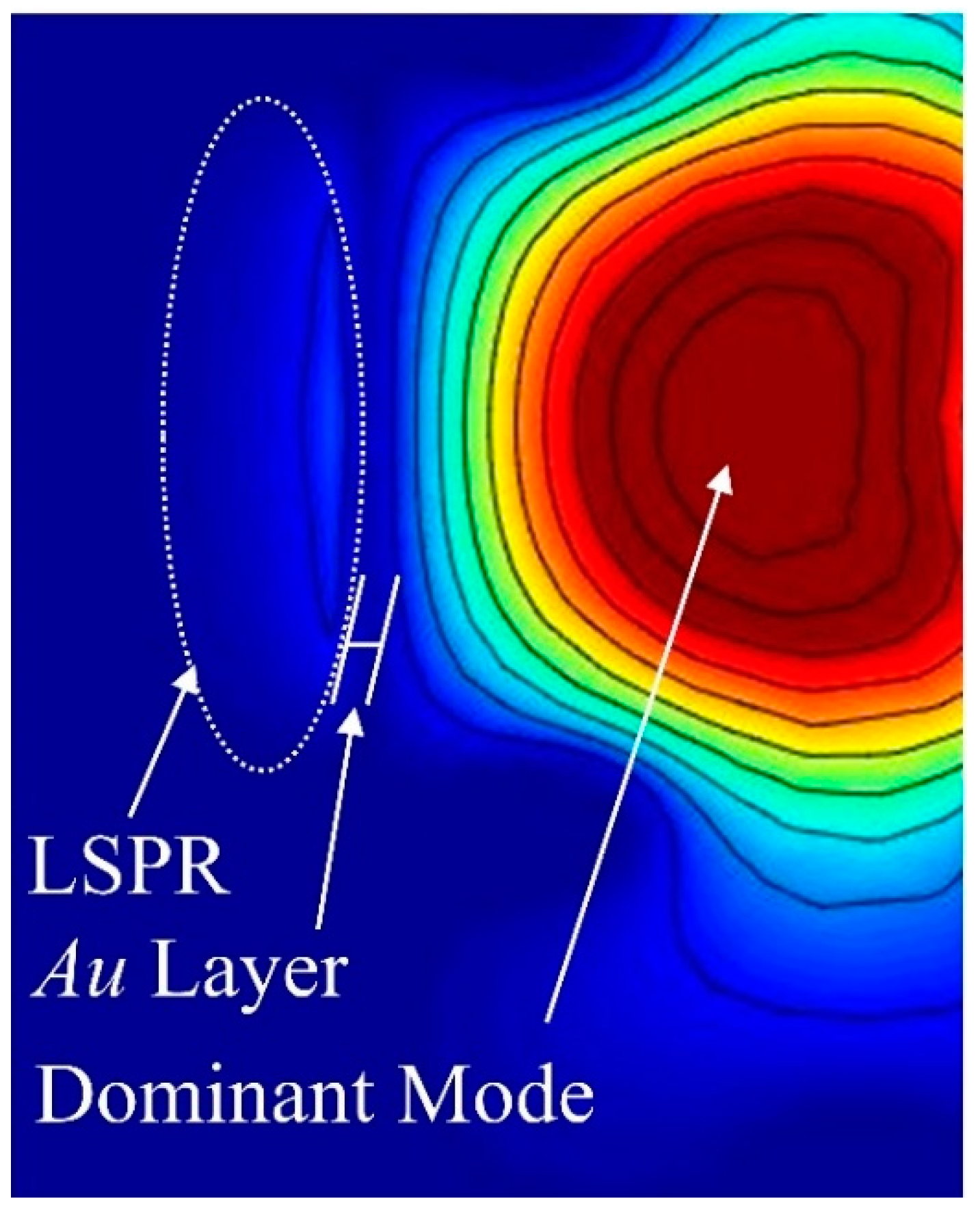
3. Results and Discussions
4. Discussion
Author Contributions
Funding
Institutional Review Board Statement
Informed Consent Statement
Acknowledgments
Conflicts of Interest
References
- Li, B.; Zhang, F.; Yan, X.; Zhang, X.; Wang, F.; Li, S.; Cheng, T. Numerical Analysis of Dual-Parameter Optical Fiber Sensor with Large Measurement Range Based on Surface Plasmon Resonance. IEEE Sens. J. 2021, 21, 10719–10725. [Google Scholar] [CrossRef]
- Wang, B.; Wang, Q. Sensitivity-Enhanced Optical Fiber Biosensor Based on Coupling Effect Between SPR and LSPR. IEEE Sens. J. 2018, 18, 8303–8310. [Google Scholar] [CrossRef]
- Sharma, A.K.; Jha, R.; Gupta, B.D. Fiber-Optic Sensors Based on Surface Plasmon Resonance: A Comprehensive Review. IEEE Sens. J. 2007, 7, 1118–1129. [Google Scholar] [CrossRef]
- Guo, X. Surface Plasmon Resonance Based Biosensor Technique: A Review. J. Biophotonics 2012, 5, 483–501. [Google Scholar] [CrossRef]
- Chen, Y.; Ming, H. Review of Surface Plasmon Resonance and Localized Surface Plasmon Resonance Sensor. Photonics Sens. 2012, 2, 37–49. [Google Scholar] [CrossRef] [Green Version]
- Paul, D.; Biswas, R. Influence of Probe Geometry of Optical Fibers in Sensing Volatile Liquids Through Localized Surface Plasmon Resonance. IEEE Trans. Nanotechnol. 2021, 20, 69–74. [Google Scholar] [CrossRef]
- Seifouri, M.; Rouini, M.A.; Olyaee, S. Design of a Surface Plasmon Resonance Biosensor Based on Photonic Crystal Fiber with Elliptical Holes. Opt. Rev. 2018, 25, 555–562. [Google Scholar] [CrossRef]
- Yasli, A.; Ademgil, H. Geometrical Comparison of Photonic Crystal Fiber-Based Surface Plasmon Resonance Sensors. Opt. Eng. 2018, 57, 030801. [Google Scholar] [CrossRef]
- Lou, J.; Cheng, T.; Li, S.; Zhang, X. Surface Plasmon Resonance Photonic Crystal Fiber Biosensor Based on Gold-Graphene Layers. Opt. Fiber Technol. 2019, 50, 206–211. [Google Scholar] [CrossRef]
- Rifat, A.A.; Mahdiraji, G.A.; Shee, Y.G.; Shawon, M.J.; Adikan, F.R.M. A Novel Photonic Crystal Fiber Biosensor Using Surface Plasmon Resonance. Procedia Eng. 2016, 140, 1–7. [Google Scholar] [CrossRef] [Green Version]
- Rifat, A.A.; Mahdiraji, Y.M.; Sua, Y.M.; Shee, Y.G.; Ahmed, R.; Chow, D.M.; Adikan, F.R.M. Surface Plasmon Resonance Photonic Crystal Fiber Biosensor: A Practical Sensing Approach. IEEE Photonics Technol. Lett. 2015, 27, 1628–1631. [Google Scholar] [CrossRef]
- Silva, J.P.; Bezerra, D.S.; Rodriguez-Esquerre, V.F.; Fonseca, I.E.; Hernández-Figueroa, H.E. Ge-Doped Defect-Core Microstructured Fiber Design by Genetic Algorithm for Residual Dispersion Compensation. IEEE Photonics Technol. Lett. 2010, 22, 1337–1339. [Google Scholar] [CrossRef]
- Tian, J.; Zhang, Q.; Fink, T.; Li, H.; Peng, W.; Han, M. Tuning Operating Point of Extrinsic Fabry-Perot Interferometric Fiber-Optic Sensors Using Microstructured Fiber and Gas Pressure. Opt. Lett. 2012, 37, 4672–4674. [Google Scholar] [CrossRef]
- Kong, D.; Wang, L. Ultrahigh-Resolution Fiber-Optic Image Guides Derived from Microstructured Polymer Optical Fiber Preforms. Opt. Lett. 2009, 34, 2435–2437. [Google Scholar] [CrossRef]
- Yan, G.; Zhang, A.P.; Ma, G.; Wang, B.; Kim, B.; Im, J.; He, S.; Chung, Y. Fiber-Optic Acetylene Gas Sensor Based on Microstructured Optical Fiber Bragg Gratings. IEEE Photonics Technol. Lett. 2011, 23, 1588–1590. [Google Scholar] [CrossRef]
- Wang, S.; Sun, X.; Luo, Y.; Peng, G. Surface Plasmon Resonance Sensor Based on D-Shaped Hi-Bi Photonic Crystal Fiber. Opt. Commun. 2020, 467, 125675. [Google Scholar] [CrossRef]
- Azkune, M.; Ayesta, I.; Ruiz-Rubio, L.; Arrospide, E.; Vilas-Vilela, J.L.; Zubia, J. Hydrogel-Core Microstructured Polymer Optical Fibers for Selective Fiber Enhanced Raman Spectroscopy. Sensors 2021, 21, 1845. [Google Scholar] [CrossRef]
- Lopez-Torres, D.; Elosua, C.; Arregui, F.J. Optical Fiber Sensors Based on Microstructured Optical Fibers to Detect Gases and Volatile Organic Compounds—A Review. Sensors 2020, 20, 2555. [Google Scholar] [CrossRef]
- Haque, E.; Hossain, M.A.; Ahmed, F.; Namihira, Y. Surface Plasmon Resonance Sensor Based on Modified D-Shaped Photonic Crystal Fiber for Wides Range of Refractive Index Detection. IEEE Sens. J. 2018, 18, 8287–8293. [Google Scholar] [CrossRef]
- Qi, M.; Zhang, N.M.Y.; Li, K.; Tjin, S.C.; Wei, L. Hybrid Plasmonic Fiber-Optic Sensors. Sensors 2020, 20, 3266. [Google Scholar] [CrossRef]
- Mo, X.; Lv, J.; Liu, Q.; Jiang, X.; Si, G. A Magnetic Field SPR Sensor Based on Temperature Self-Reference. Sensors 2021, 21, 6130. [Google Scholar] [CrossRef]
- Melwin, G.; Senthilnathan, K. High Sensitive D-Shaped Photonic Crystal Fiber Sensor with V-Groove Analyte Channel. Int. J. Light Electron. Opt. 2020, 213, 164779. [Google Scholar] [CrossRef]
- Portosi, V.; Laneve, D.; Falconi, M.C.; Prudenzano, F. Advances on Photonic Crystal Fiber Sensors and Applications. Sensors 2019, 19, 1892. [Google Scholar] [CrossRef] [Green Version]
- Han, H.; Hou, D.; Luan, N.; Bai, Z.; Song, L.; Liu, J.; Hu, Y. Surface Plasmon Resonance Sensor Based on Dual-Side Polished Microstructured Optical Fiber with Dual-Core. Sensors 2020, 20, 3911. [Google Scholar] [CrossRef]
- Shrivastav, A.M.; Gunawardena, D.S.; Liu, Z.; Tam, H. Microstructured Optical Fiber Based Fabry-Pérot Interferometer as a Humidity Sensor Utilizing Chitosan Polymeric Matrix for Breath Monitoring. Sci. Rep. 2020, 10, 6002. [Google Scholar] [CrossRef]
- Antonio-Lopez, J.E.; Eznaveh, Z.S.; LiKamWa, P.; Schülzgen, A.; Amezcua-Correa, R. Multicore Fiber Sensor for High-Temperature Applications up to 1000 °C. Opt. Lett. 2014, 39, 4309–4312. [Google Scholar] [CrossRef]
- Monfared, Y.E.; Hajati, M.; Liang, C.; Qasymeh, M. Quasi-D-Shaped Fiber Optic Plasmonic Biosensor for High-Index Analyte Detection. IEEE Sens. J. 2021, 21, 17–23. [Google Scholar] [CrossRef]
- Mahfuz, M.A.; Hossain, M.A.; Haque, E.; Hai, N.H.; Namihira, Y.; Ahmed, F. Dual-Core Photonic Crystal Fiber-Based Plasmonic RI Sensor in the Visible to Near-IR Operating Band. IEEE Sens. J. 2020, 20, 7692–7700. [Google Scholar] [CrossRef]
- Luan, N.; Zhao, L.; Lian, Y.; Lou, S. A High Refractive Index Plasmonic Sensor Based on D-Shaped Photonic Crystal Fiber with Laterally Accessible Hollow-Core. IEEE Photonics J. 2018, 10, 6803707. [Google Scholar] [CrossRef]
- Haider, F.; Aoni, R.A.; Ahmed, R.; Islam, M.S.; Miroshnichenko, E. Propagation Controlled Photonic Crystal Fiber Based Plasmonic Sensor via Scaled-Down Approach. IEEE Sens. J. 2019, 19, 962–969. [Google Scholar] [CrossRef]
- Fan, Z.; Li, S.; Liu, Q.; An, G.; Chen, H.; Li, J.; Chao, D.; Li, H.; Zi, J.; Tian, W. High-Sensitivity of Refractive Index Sensor Based on Analyte-Filled Photonic Crystal Fiber with Surface Plasmon Resonance. IEEE Photonics J. 2015, 7, 2432079. [Google Scholar] [CrossRef]
- White, T.P.; McPhedran, R.C.; Sterke, C.M.; Botten, L.C.; Steel, M.J. Confinement Losses in Microstructured Optical Fibers. Opt. Lett. 2001, 26, 1660–1662. [Google Scholar] [CrossRef]
- da Silva, J.P. Simulação por Elementos Finitos de Propagação de Feixes Ópticos em Estruturas Fotônicas. Ph.D. Thesis, Campinas State University—UNICAMP, Campinas, Brazil, 11 April 2013. [Google Scholar]
- Gauvreau, B.; Hassani, A.; Fehri, M.F.; Kabashin, A.; Skorobogatiy, M. Photonic Bandgap Fiber-Based Surface Plasmon Resonance Sensors. Opt. Express 2007, 15, 11413–11426. [Google Scholar] [CrossRef] [Green Version]
- Brückner, V. To the Use of Sellmeier Formula. In Elements of Optical Networking: Basics and Practice of Optical Data Communication, 1st ed.; Brückner, V., Ed.; Springer: Berlin/Heidelberg, Germany, 2011; Volume 1, p. 194. [Google Scholar]
- Rakić, A.D.; Djurišić, A.B.; Elazar, J.M.; Majewski, M.L. Optical Proprieties of Metallic Films for Vertical-Cavity Optoelectronic Devices. Appl. Opt. 1998, 37, 5271–5283. [Google Scholar] [CrossRef]


| Sensors | ||||||
|---|---|---|---|---|---|---|
| No doping | 0.6961663 | 0.4079426 | 0.8974794 | 0.0684043 | 0.1162414 | 9.896161 |
| 0.6867178 | 0.4348151 | 0.8956551 | 0.0726752 | 0.1151435 | 10.002398 | |
| 0.7083925 | 0.4203993 | 0.8663412 | 0.0853842 | 0.1024839 | 9.896175 | |
| 0.73454395 | 0.4271083 | 0.8210340 | 0.00869769 | 0.1119519 | 10.48654 | |
| 0.7347008 | 0.4461191 | 0.8081698 | 0.0764679 | 0.1246081 | 9.896203 |
| No Doping | (4.1%) | (6.3%) | (13.5%) | (19.3%) | |
|---|---|---|---|---|---|
| 0.80 | 1.4533172548 | 1.4596845495 | 1.4622823847 | 1.4715515550 | 1.4810033015 |
| 0.85 | 1.4524982860 | 1.4588361870 | 1.4614292333 | 1.4709993384 | 1.4800696281 |
| 0.90 | 1.4517539550 | 1.4580689419 | 1.4606585052 | 1.4704900422 | 1.4792367010 |
| 0.95 | 1.4510651315 | 1.4573624396 | 1.4599496556 | 1.4700118200 | 1.4784802919 |
| 1.00 | 1.4504174094 | 1.4567013392 | 1.4592871988 | 1.4695557639 | 1.4777821857 |
| 1.05 | 1.4497997593 | 1.4560738981 | 1.4586592708 | 1.4691150616 | 1.4771284601 |
| 1.10 | 1.4492036097 | 1.4554709933 | 1.4580566479 | 1.4686844229 | 1.4765083153 |
| 1.15 | 1.4486222069 | 1.4548854402 | 1.4574720609 | 1.4682596813 | 1.4759132590 |
| 1.20 | 1.4480501614 | 1.4543115084 | 1.4568997094 | 1.4678375126 | 1.4753365304 |
| 1.25 | 1.4474831206 | 1.4537445737 | 1.4563349105 | 1.4674152314 | 1.4747726841 |
| 1.30 | 1.4469175294 | 1.4531808627 | 1.4557738414 | 1.4669906435 | 1.4742172864 |
| 1.35 | 1.4463504523 | 1.4526172632 | 1.4552133484 | 1.4665619352 | 1.4736666904 |
| 1.40 | 1.4457794402 | 1.4520511825 | 1.4546508033 | 1.4661275918 | 1.4731178664 |
| 1.45 | 1.4452024286 | 1.4514804385 | 1.4540839942 | 1.4656863342 | 1.4725682741 |
| 1.50 | 1.4446176596 | 1.4509031772 | 1.4535110411 | 1.465237071 | 1.4720157629 |
| 1.55 | 1.4440236217 | 1.4503178079 | 1.4529303310 | 1.4647788624 | 1.4714584966 |
| 1.60 | 1.4434190019 | 1.4497229527 | 1.4523404668 | 1.4643108884 | 1.4708948926 |
| 1.65 | 1.4428026489 | 1.4491174068 | 1.4517402268 | 1.4638324286 | 1.4703235752 |
| 1.70 | 1.4421735426 | 1.4485001066 | 1.4511285325 | 1.4633428423 | 1.4697433377 |
| 1.75 | 1.4415307705 | 1.4478701039 | 1.4505044226 | 1.4628415542 | 1.4691531123 |
| 1.80 | 1.4408735085 | 1.4472265460 | 1.4498670326 | 1.4623280424 | 1.4685519459 |
| 1.85 | 1.4402010046 | 1.4465686581 | 1.4492155773 | 1.4618018289 | 1.4679389798 |
| 1.90 | 1.4395125664 | 1.4458957302 | 1.4485493372 | 1.4612624715 | 1.4673134341 |
| 1.95 | 1.4388075504 | 1.4452071054 | 1.4478676464 | 1.4607095576 | 1.4666745939 |
| 2.00 | 1.4380853528 | 1.4445021703 | 1.4471698840 | 1.4601426981 | 1.4660217981 |
| Doping | WS_Total (nm/RIU) | (nm/RIU) | |||
|---|---|---|---|---|---|
| No doping (0%) | 1.35 | 11,374.41 | 4744.96 | 24,691.36 | 80,000.00 |
| 1.36 | 11,352.89 | 4756.24 | 24,242.42 | 78,431.37 | |
| 1.37 | 11,538.46 | 4872.11 | 23,952.09 | 76,923.07 | |
| 1.38 | 11,695.90 | 4884.00 | 23,391.81 | 111,111.11 | |
| 1.39 | 11,869.43 | 5012.53 | 22,727.27 | 108,108.11 | |
| 1.40 | 12,060.30 | 4987.53 | 25,974.02 | 102,564.10 | |
| 1.41 | 11,764.70 | 4987.53 | 25,000.00 | 68,965.52 | |
| 1.42 | 12,133.47 | 5154.63 | 23,952.09 | 86,956.52 | |
| 1.43 | 11,111.11 | 5376.34 | 22,857.14 | 24,844.72 | |
| 1.35 | 9554.14 | 4901.96 | 11,627.90 | 41,666.66 | |
| 1.36 | 9508.72 | 4884.00 | 11,527.37 | 41,666.66 | |
| 1.37 | 9538.95 | 4932.18 | 11,396.01 | 41,666.66 | |
| 1.38 | 9463.72 | 4907.97 | 11,204.48 | 41,666.66 | |
| 1.39 | 9493.67 | 4968.94 | 11,019.28 | 41,666.66 | |
| 1.40 | 9516.26 | 5044.13 | 10,752.68 | 41,666.66 | |
| 1.41 | 9382.33 | 5174.64 | 9779.95 | 41,237.11 | |
| 1.42 | 9167.30 | 5095.54 | 10,050.25 | 31,746.03 | |
| 1.43 | 9811.94 | 5235.60 | 9546.54 | 100,000.00 | |
| 1.44 | 9900.99 | 5641.74 | 18,099.54 | 14,184.39 | |
| 1.33 | 9463.72 | 4938.27 | 11,695.90 | 34,482.75 | |
| 1.34 | 9360.37 | 4866.18 | 11,627.90 | 34,482.75 | |
| 1.35 | 9382.32 | 4901.96 | 11,527.37 | 34,482.75 | |
| 1.36 | 9331.25 | 4878.04 | 11,428.57 | 34,482.75 | |
| 1.37 | 9367.68 | 4932.18 | 11,299.43 | 34,482.75 | |
| 1.38 | 9295.12 | 4907.97 | 11,111.11 | 34,482.75 | |
| 1.39 | 9324.00 | 4968.94 | 10,928.96 | 34,482.75 | |
| 1.40 | 9338.52 | 5208.33 | 9975.06 | 34,482.75 | |
| 1.41 | 9216.58 | 5174.64 | 9708.73 | 34,188.03 | |
| 1.42 | 9167.30 | 5095.54 | 9950.24 | 32,786.88 | |
| 1.43 | 9787.92 | 5228.75 | 9546.53 | 95,238.09 | |
| 1.32 | 9577.01 | 5188.06 | 10,025.06 | 48,192.77 | |
| 1.33 | 9478.67 | 5115.08 | 9975.06 | 48,192.77 | |
| 1.34 | 9375.00 | 5044.13 | 9900.99 | 48,192.77 | |
| 1.35 | 9389.67 | 5069.70 | 9876.54 | 47,619.04 | |
| 1.36 | 9331.25 | 5044.13 | 9779.95 | 47,619.04 | |
| 1.37 | 9353.07 | 5089.05 | 9685.23 | 47,619.04 | |
| 1.38 | 9273.57 | 5050.50 | 9569.37 | 47,619.04 | |
| 1.39 | 9287.92 | 5108.55 | 9411.76 | 47,619.04 | |
| 1.40 | 9295.12 | 5167.95 | 9237.87 | 47,619.04 | |
| 1.41 | 9042.95 | 4889.97 | 9803.92 | 39,603.96 | |
| 1.42 | 9153.32 | 5141.39 | 8869.18 | 48,780.48 | |
| 1.43 | 9324.01 | 5263.16 | 8928.57 | 50,632.91 | |
| 1.44 | 10,058.67 | 5376.34 | 8583.69 | 235,294.12 | |
| 1.32 | 9748.17 | 5181.34 | 9324.00 | 133,333.33 | |
| 1.33 | 9654.06 | 5115.08 | 9280.74 | 133,333.33 | |
| 1.34 | 9546.53 | 5044.13 | 9216.58 | 133,333.33 | |
| 1.35 | 9486.16 | 5012.53 | 9153.31 | 133,333.33 | |
| 1.36 | 9389.67 | 4950.49 | 9090.90 | 133,333.33 | |
| 1.37 | 9345.79 | 4938.27 | 9009.00 | 133,333.33 | |
| 1.38 | 9230.76 | 4872.10 | 8908.68 | 133,333.33 | |
| 1.39 | 9181.33 | 4866.18 | 8791.20 | 133,333.33 | |
| 1.40 | 9118.54 | 4866.18 | 8620.68 | 133,333.33 | |
| 1.41 | 8961.91 | 4796.16 | 8421.05 | 133,333.33 | |
| 1.42 | 8658.00 | 4739.33 | 8368.20 | 62,500.00 | |
| 1.43 | 8778.34 | 4790.41 | 8733.62 | 54,054.05 | |
| 1.44 | 8670.52 | 4981.32 | 9280.74 | 26,666.66 | |
| 1.45 | 9448.81 | 5319.14 | 8048.28 | 190,476.19 |
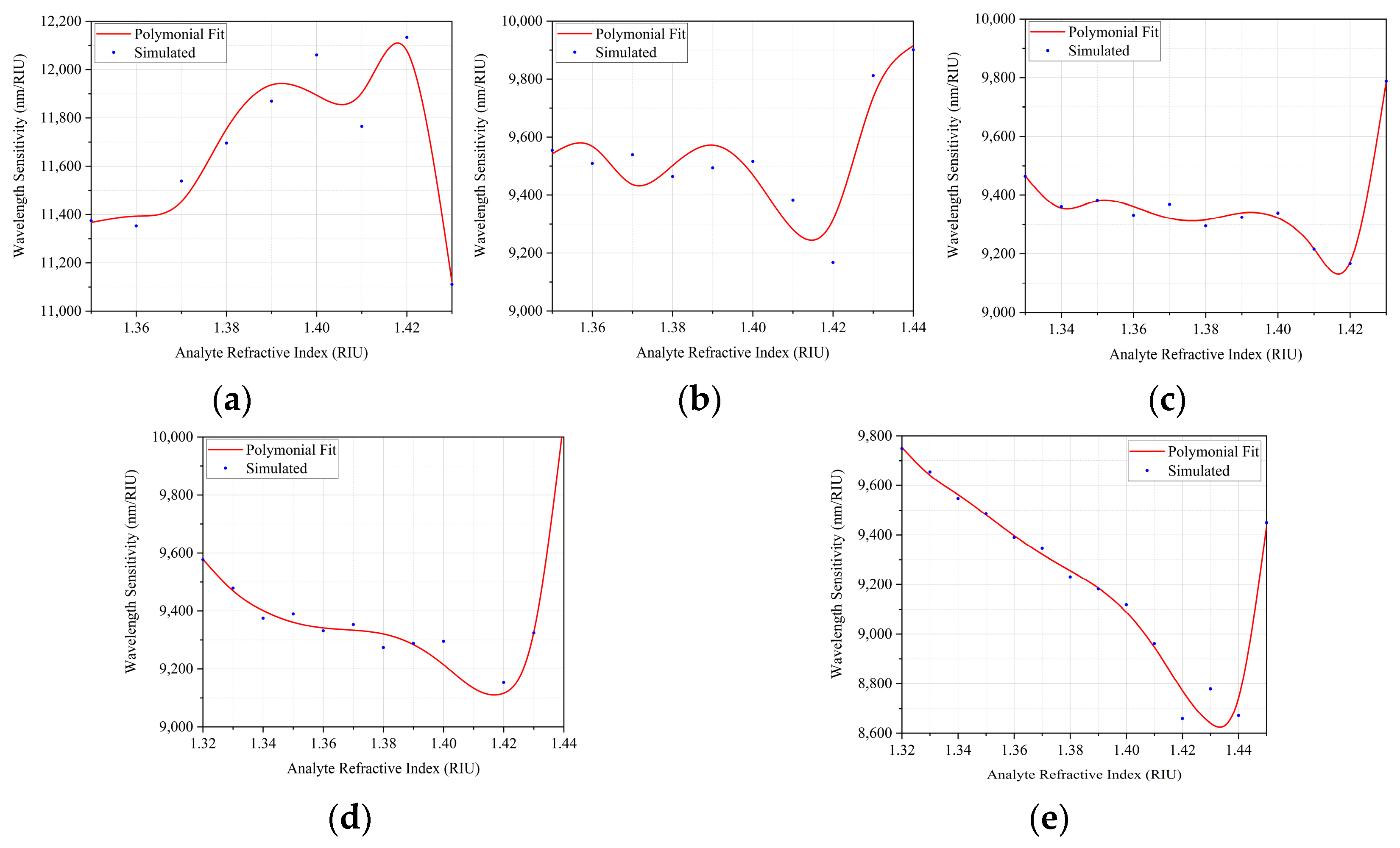
| Figure | Polynomials |
|---|---|
| Figure 11a | |
| Figure 11b | |
| Figure 11c | |
| Figure 11d | |
| Figure 11e |
| References | Type of Sensing | RI Range | ||||
|---|---|---|---|---|---|---|
| [8] | External | 1.33–1.35 | 3558.33 | 4200.00 | ||
| [18] | Internal | 1.33–1.42 | 11,000.00 | |||
| [27] | External | 1.45–1.60 | 3000.00 | 4800.00 | 11,800.00 | |
| [28] | External | 1.33–1.42 | 80.00 | 28,000.00 | ||
| [29] | External | 1.43–1.48 | 35.00 | 7200.00 | 10,000.00 | |
| [30] | External | 1.33–1.39 | 296.00 | 22,000.00 | ||
| [31] | Internal | 1.33–1.38 | 2000.00 | 4600.00 | 7040.00 | |
| This Work | No doping | External | 1.35–1.43 | 2100.00 | 11,650.63 | 12,133.47 |
| External | 1.35–1.44 | 530.00 | 9533.80 | 9900.99 | ||
| External | 1.33–1.43 | 1980.00 | 9366.80 | 9787.92 | ||
| External | 1.32–1.44 | 600.00 | 9380.02 | 10,058.67 | ||
| External | 1.32–1.45 | 2000.00 | 9229.90 | 9748.17 | ||
Publisher’s Note: MDPI stays neutral with regard to jurisdictional claims in published maps and institutional affiliations. |
© 2022 by the authors. Licensee MDPI, Basel, Switzerland. This article is an open access article distributed under the terms and conditions of the Creative Commons Attribution (CC BY) license (https://creativecommons.org/licenses/by/4.0/).
Share and Cite
Cunha, N.H.O.; Da Silva, J.P. High Sensitivity Surface Plasmon Resonance Sensor Based on a Ge-Doped Defect and D-Shaped Microstructured Optical Fiber. Sensors 2022, 22, 3220. https://doi.org/10.3390/s22093220
Cunha NHO, Da Silva JP. High Sensitivity Surface Plasmon Resonance Sensor Based on a Ge-Doped Defect and D-Shaped Microstructured Optical Fiber. Sensors. 2022; 22(9):3220. https://doi.org/10.3390/s22093220
Chicago/Turabian StyleCunha, Nilson H. O., and José P. Da Silva. 2022. "High Sensitivity Surface Plasmon Resonance Sensor Based on a Ge-Doped Defect and D-Shaped Microstructured Optical Fiber" Sensors 22, no. 9: 3220. https://doi.org/10.3390/s22093220
APA StyleCunha, N. H. O., & Da Silva, J. P. (2022). High Sensitivity Surface Plasmon Resonance Sensor Based on a Ge-Doped Defect and D-Shaped Microstructured Optical Fiber. Sensors, 22(9), 3220. https://doi.org/10.3390/s22093220