A Configurable and Fully Synthesizable RTL-Based Convolutional Neural Network for Biosensor Applications

 , ,
, , 
Abstract
1. Introduction
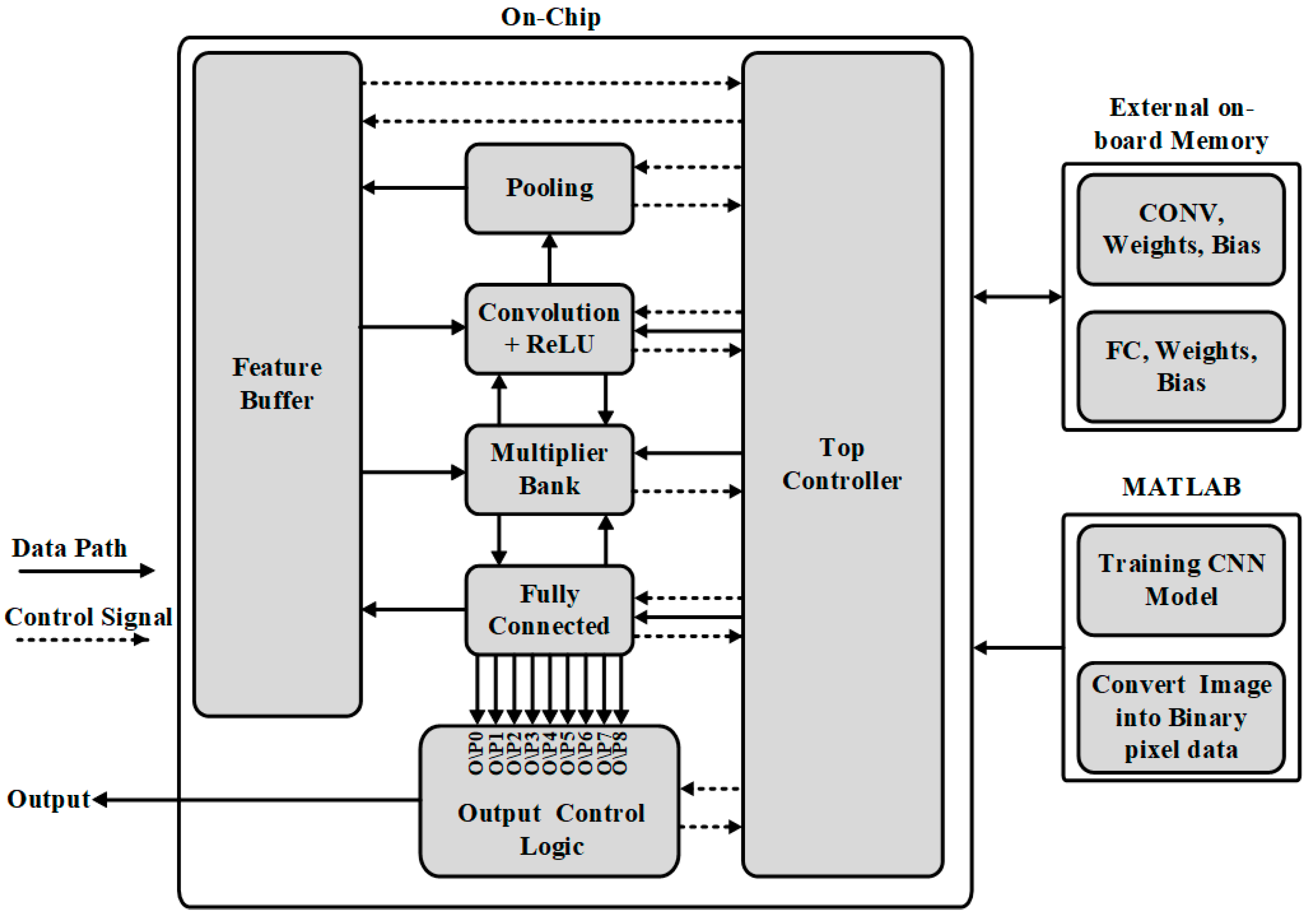
2. Top Architecture
3. Building Blocks
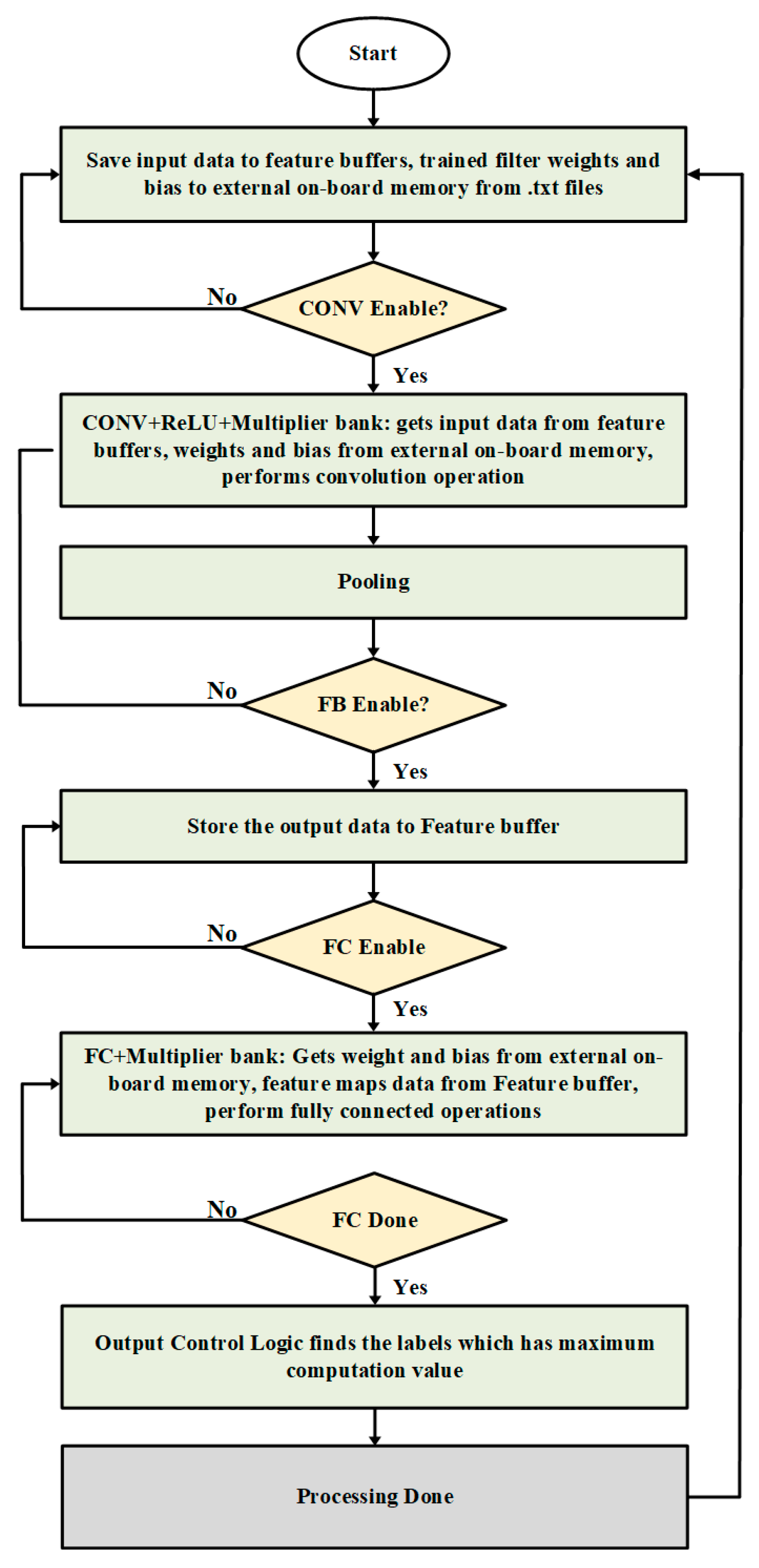
3.1. Top Controller
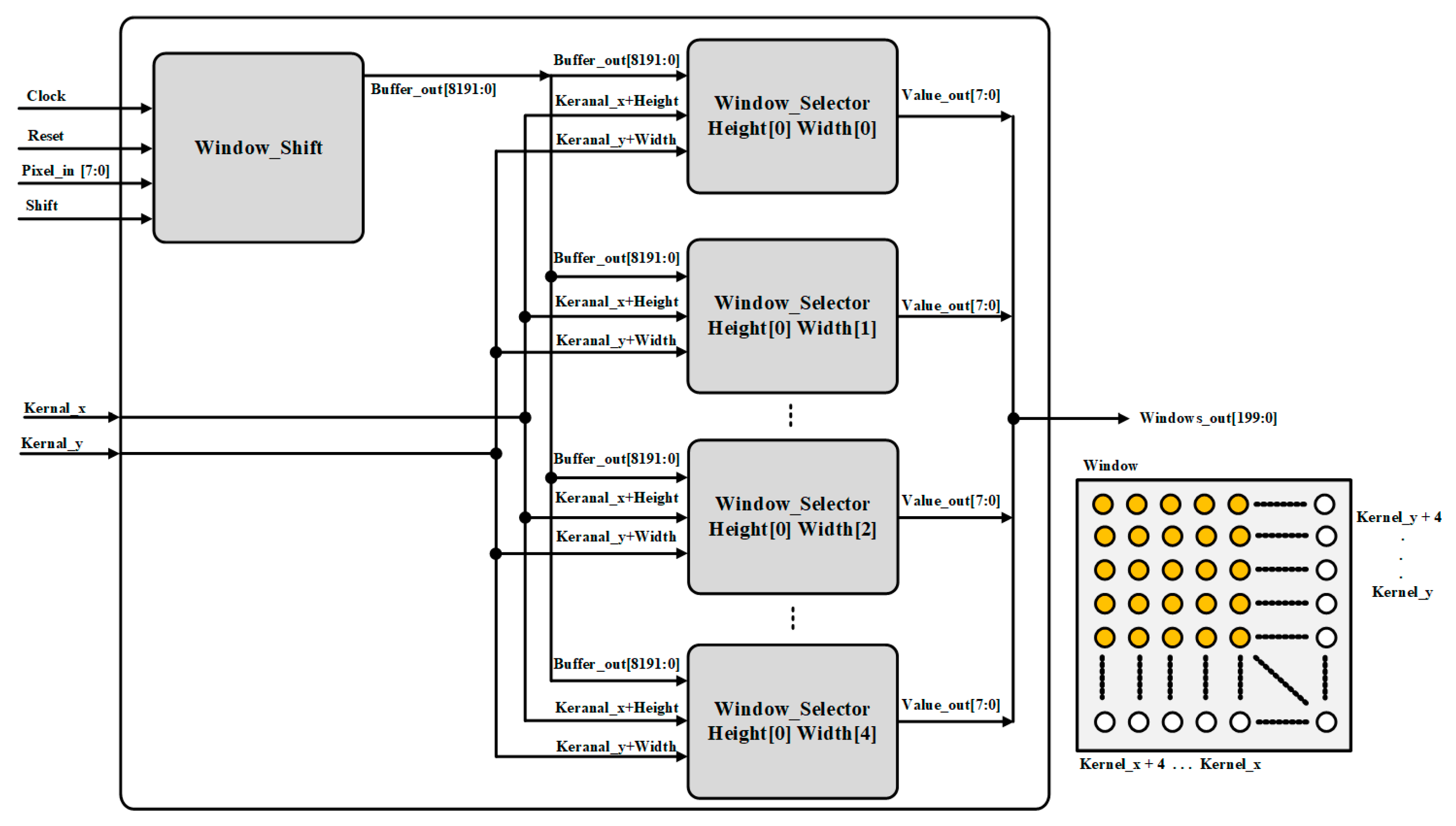
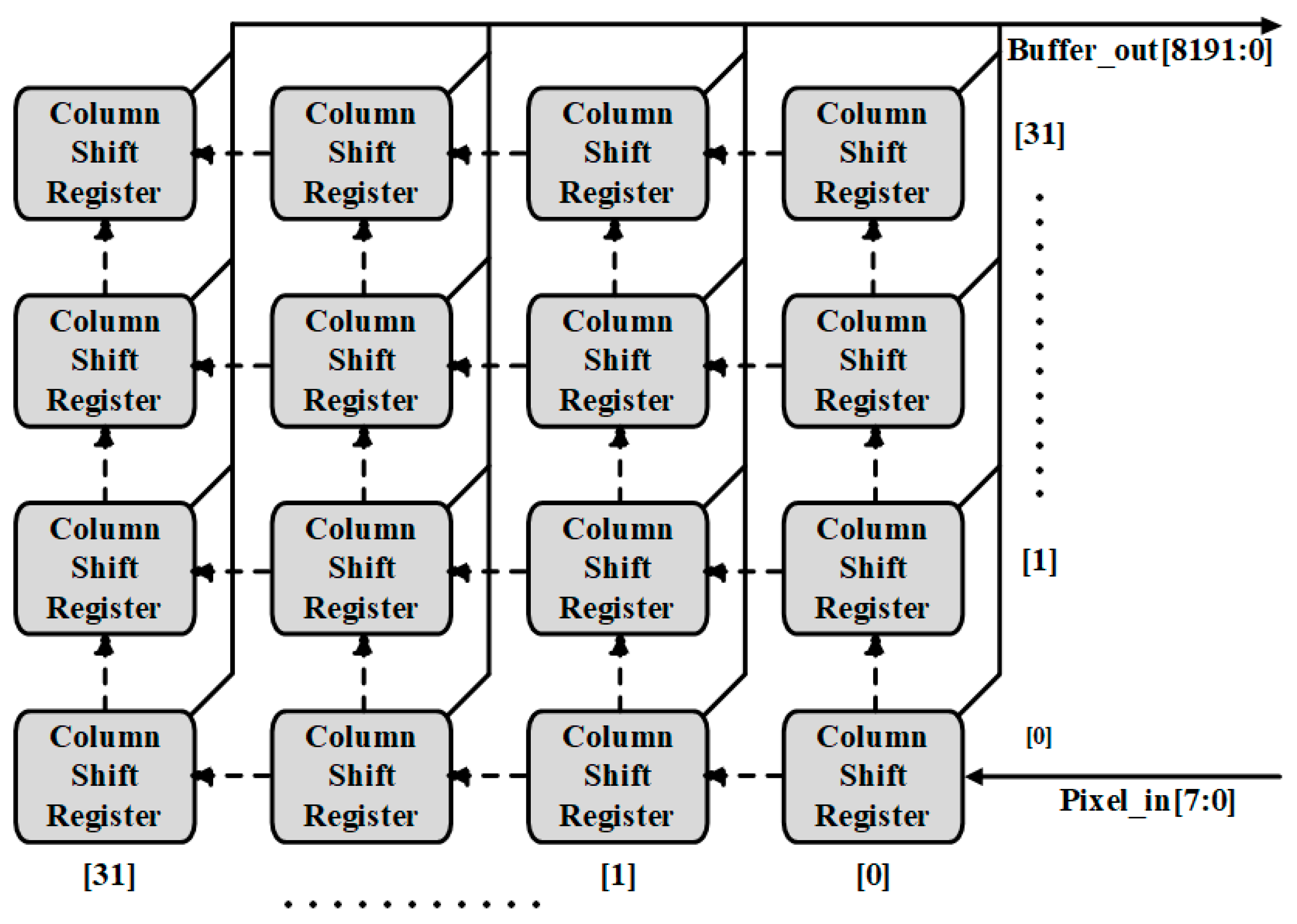
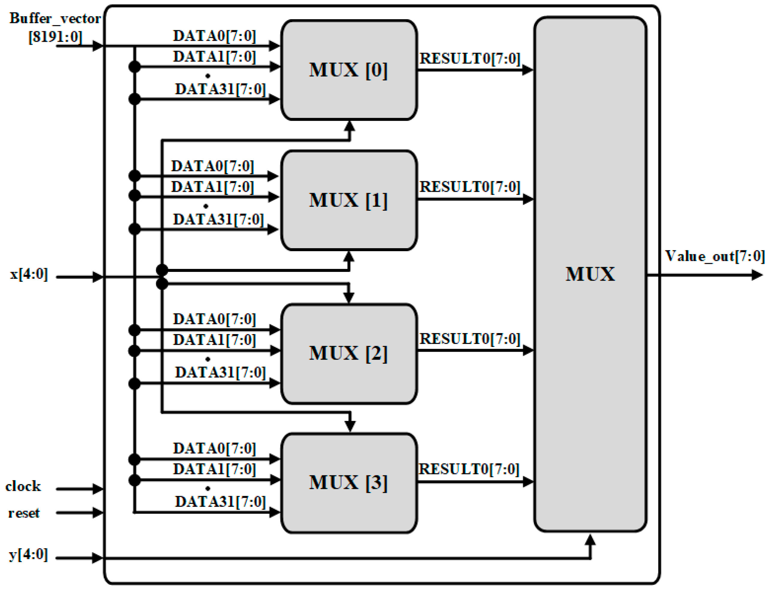
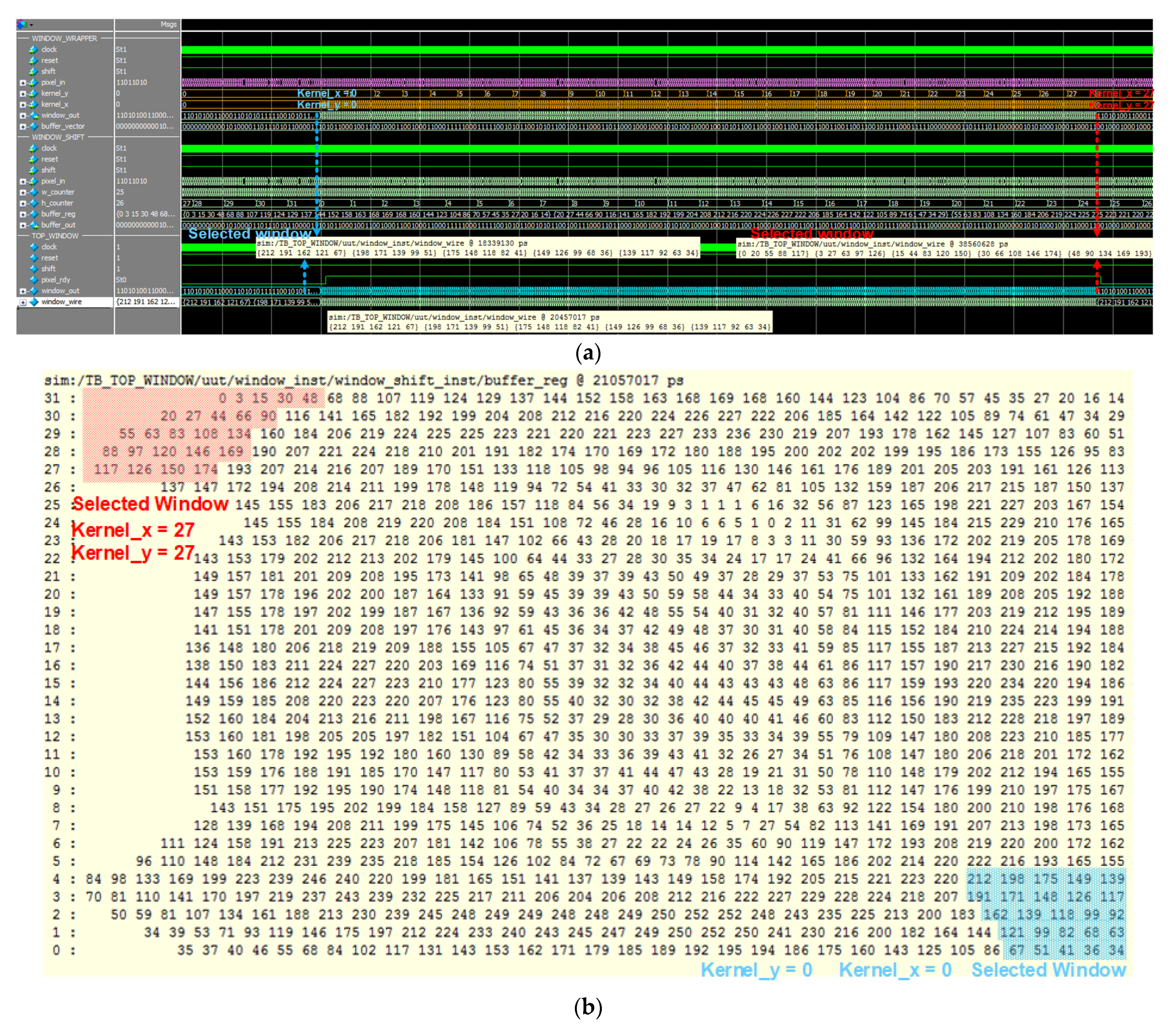
3.2. Feature Buffers
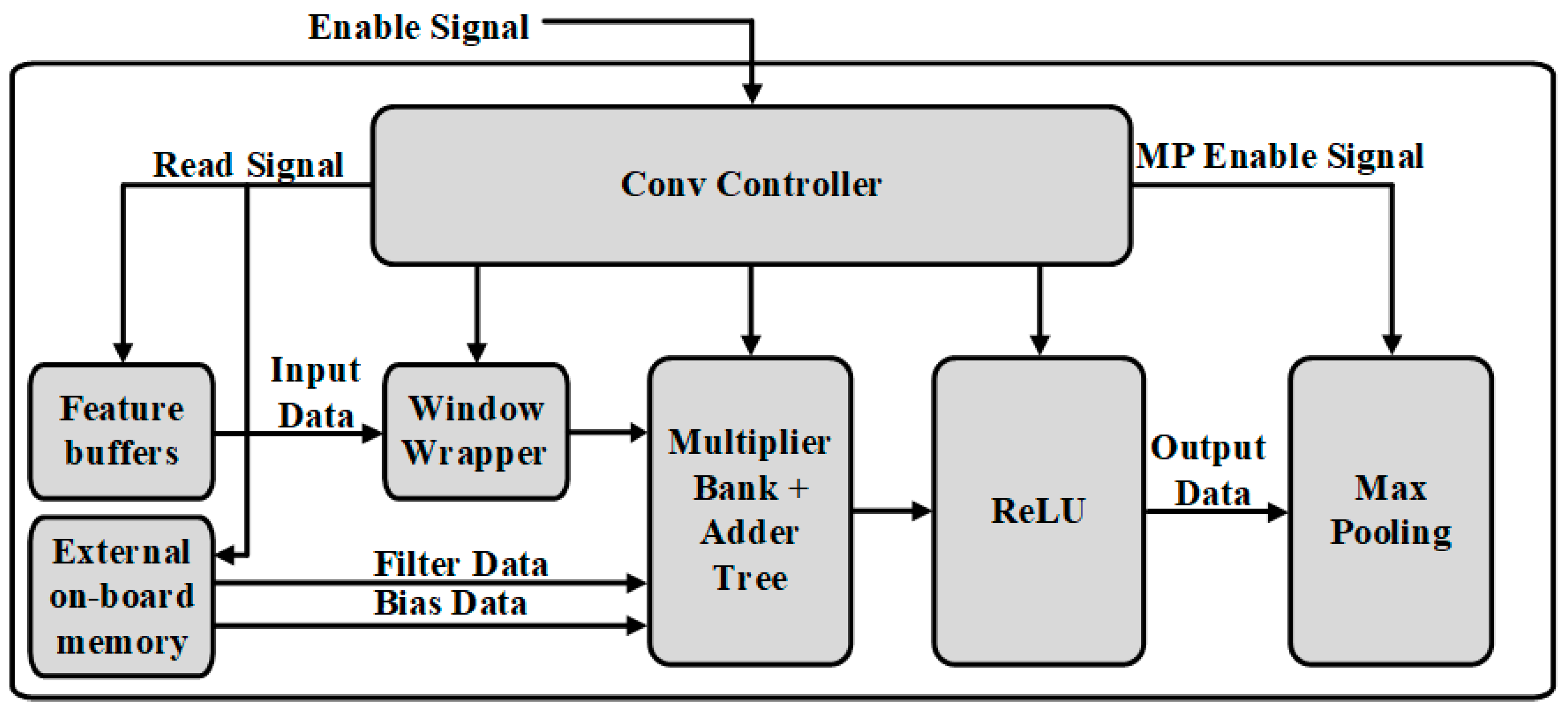
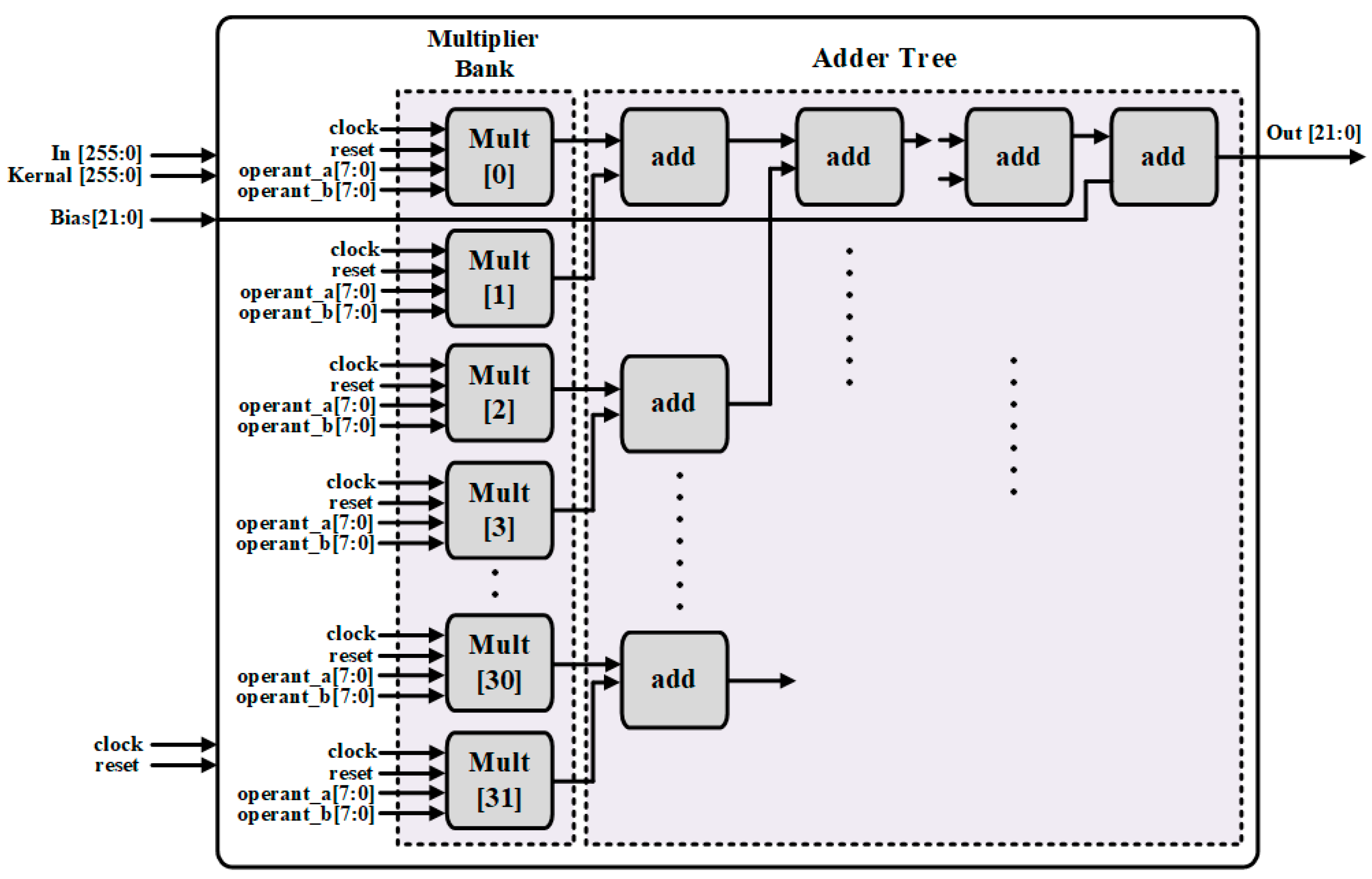
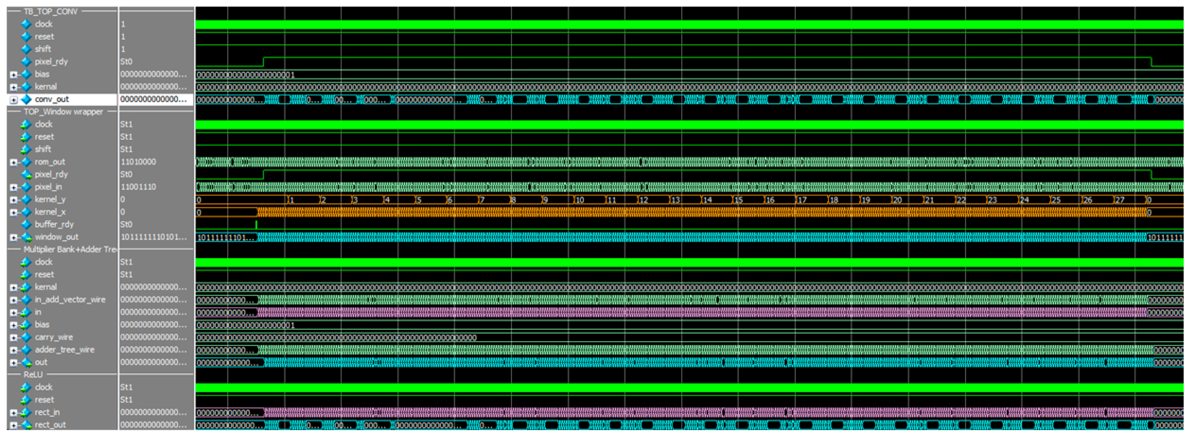
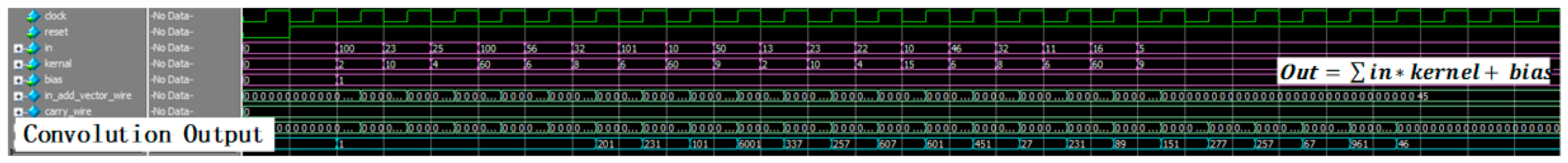
3.3. Convolutional Operation
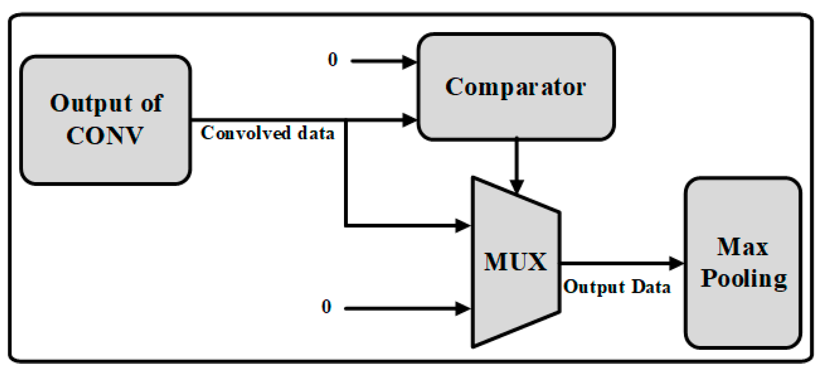
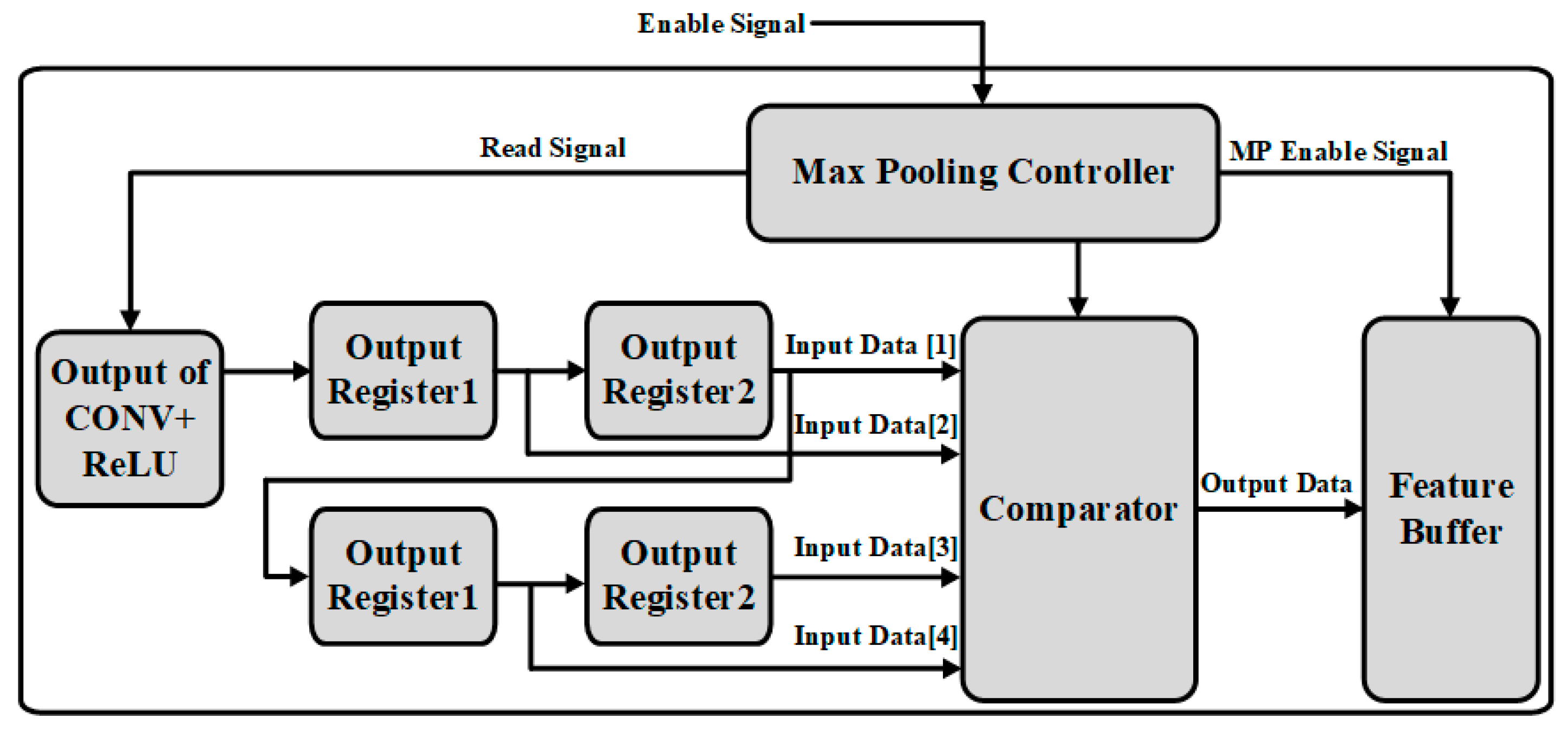
3.4. Max-Pooling Operation
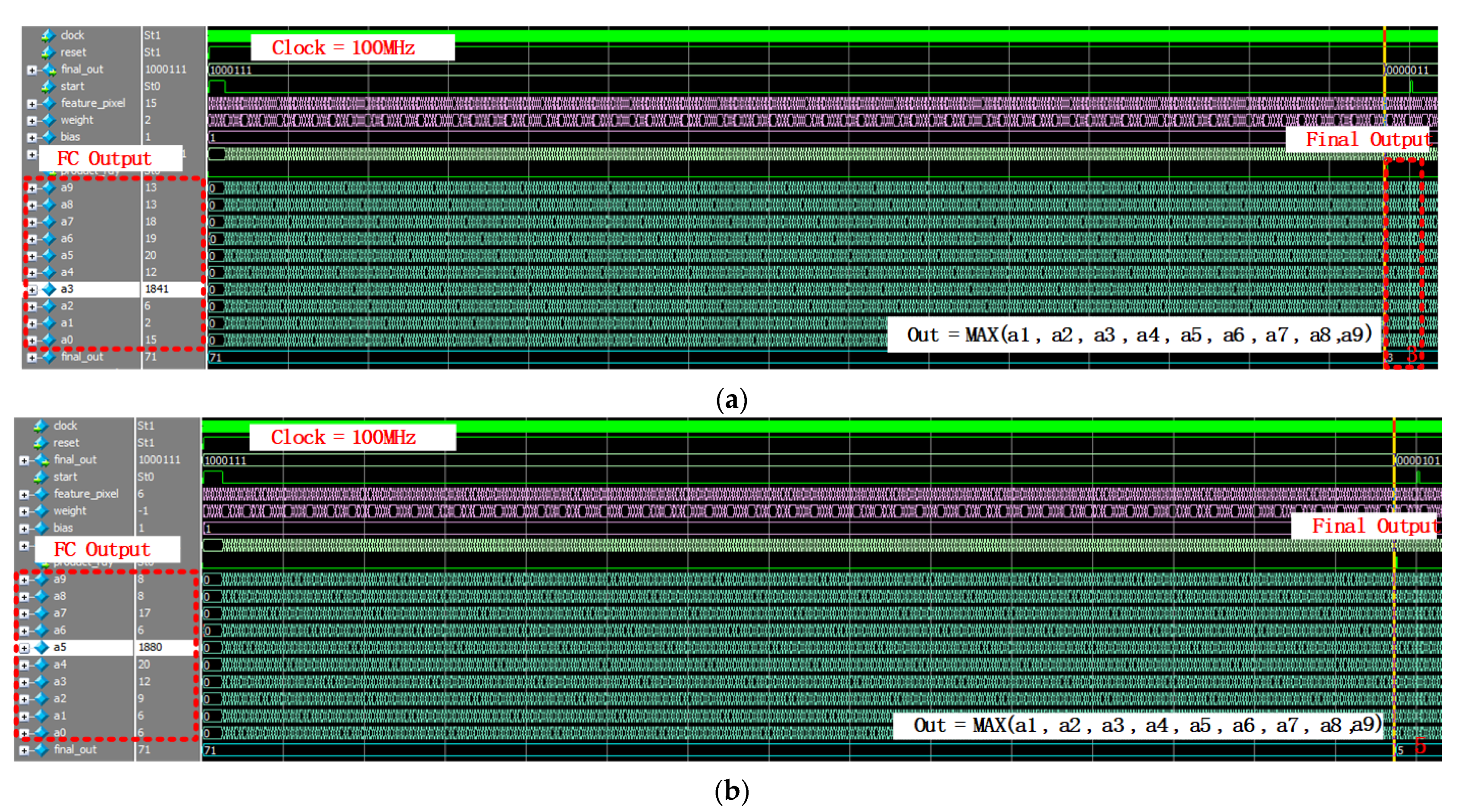
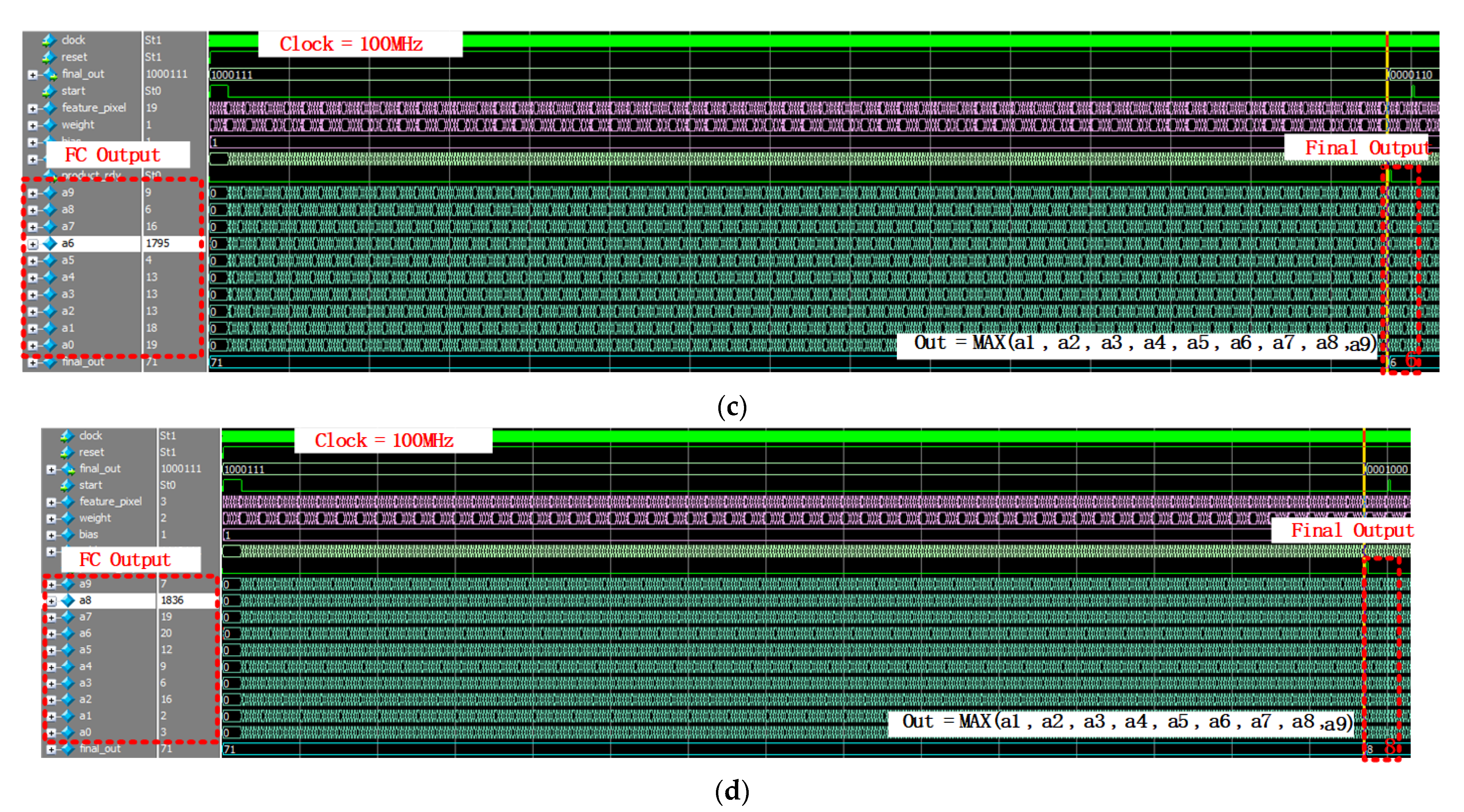
3.5. Fully Connected Operation
4. Experimental Results
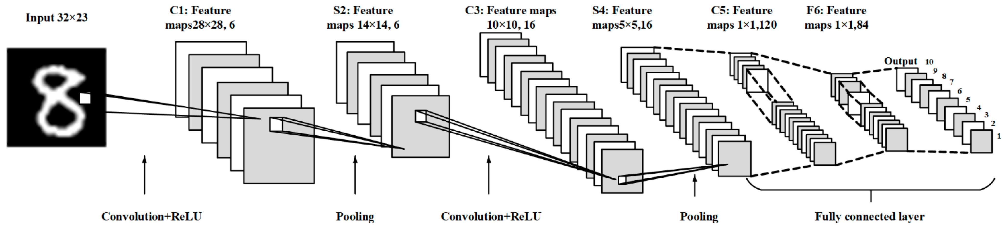
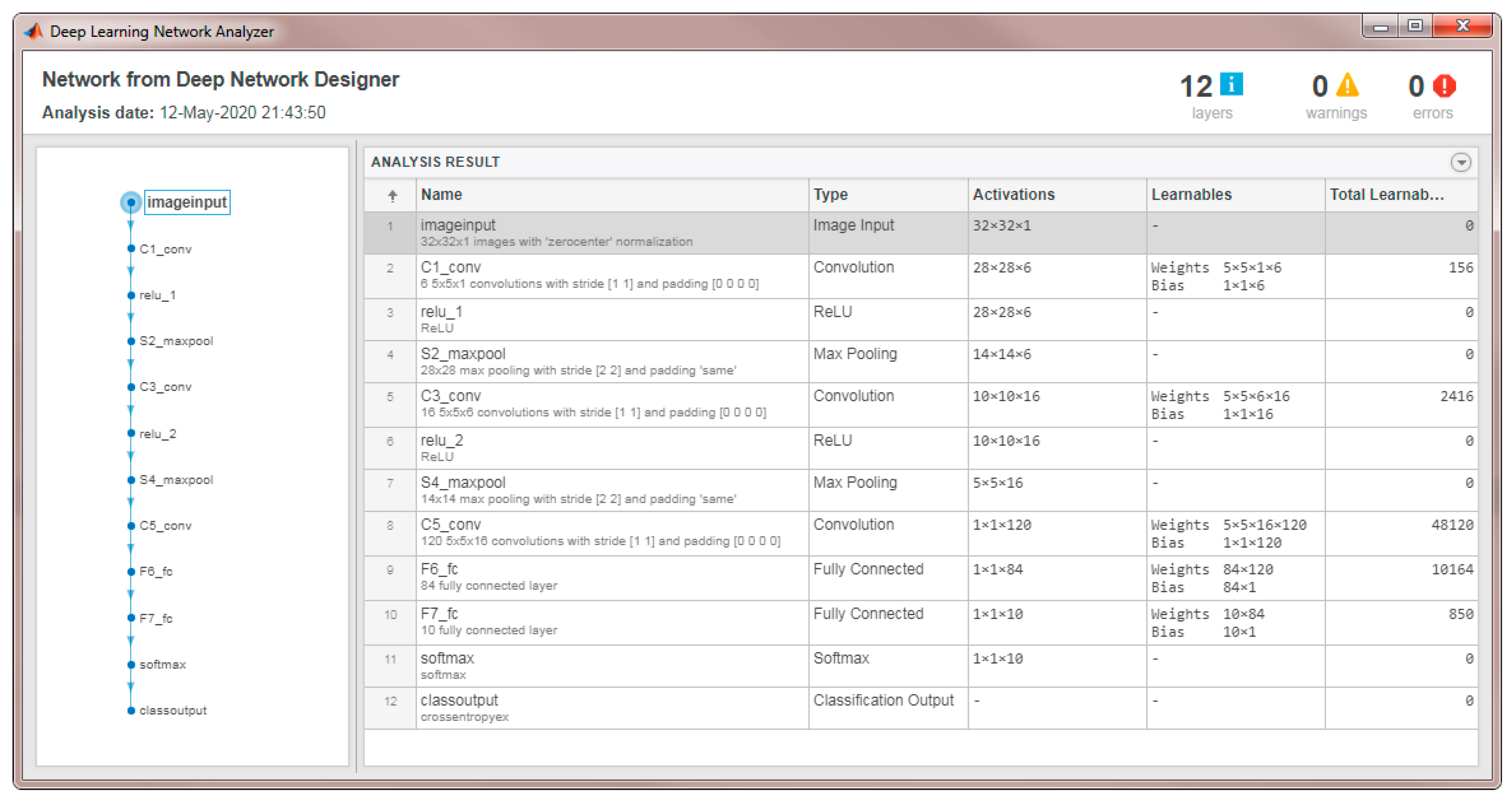
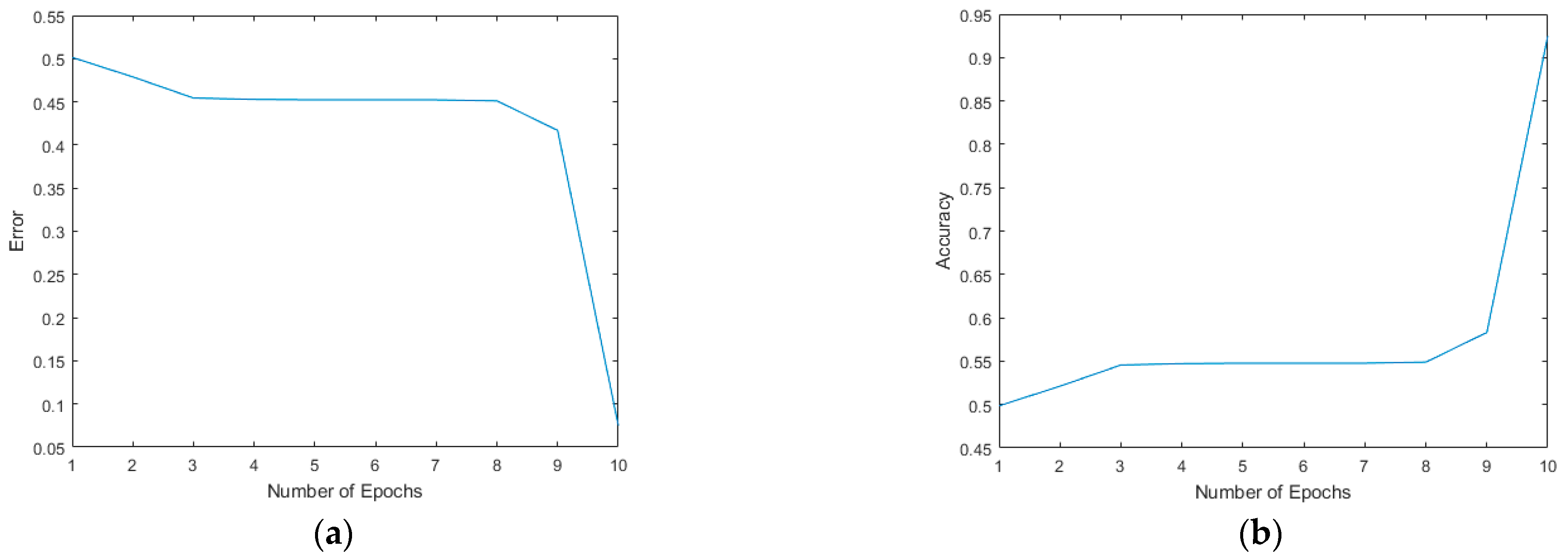
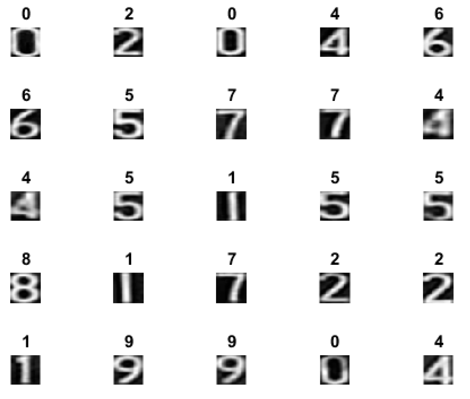
4.1. MATLAB® Modeling and Results
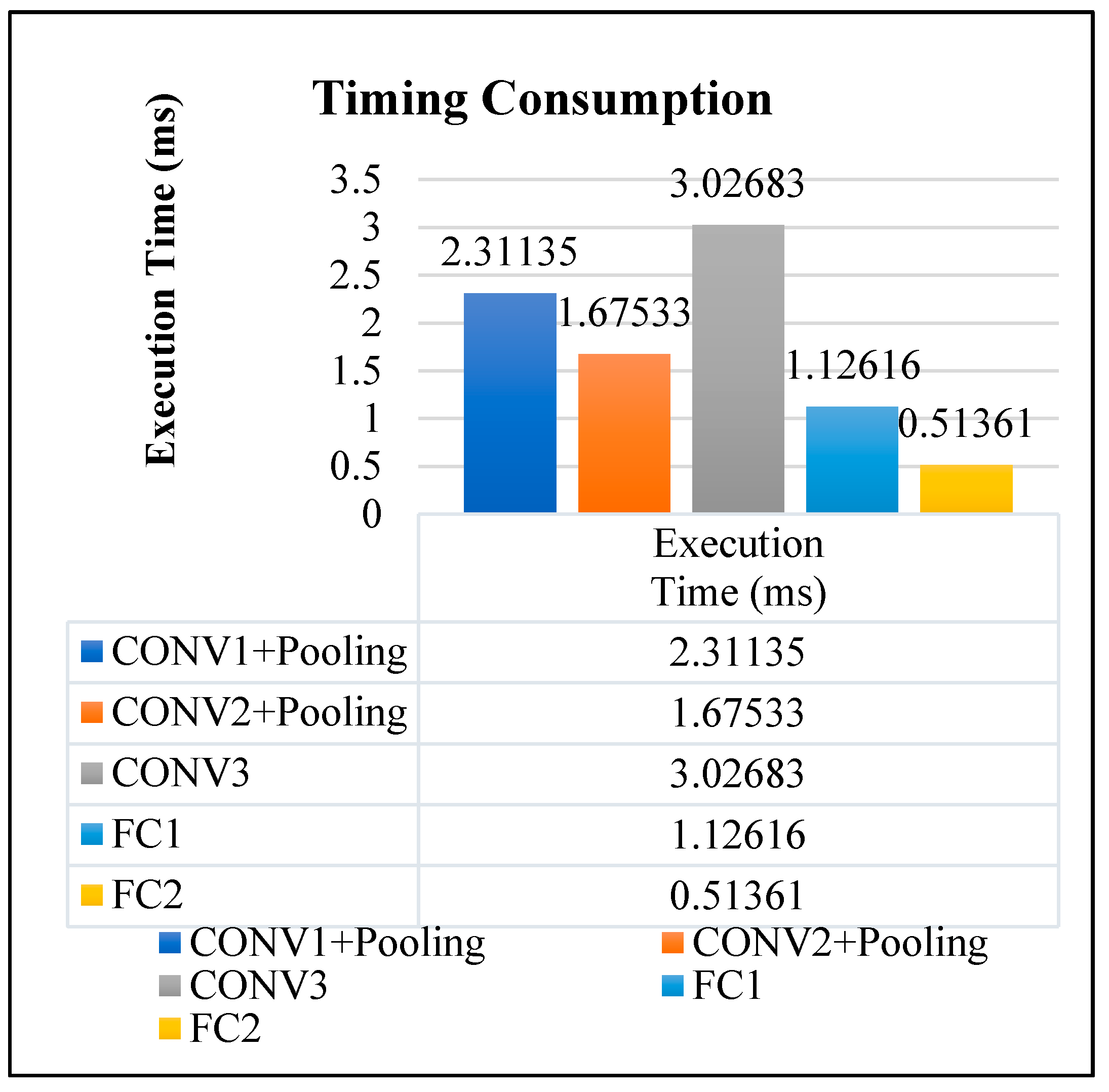
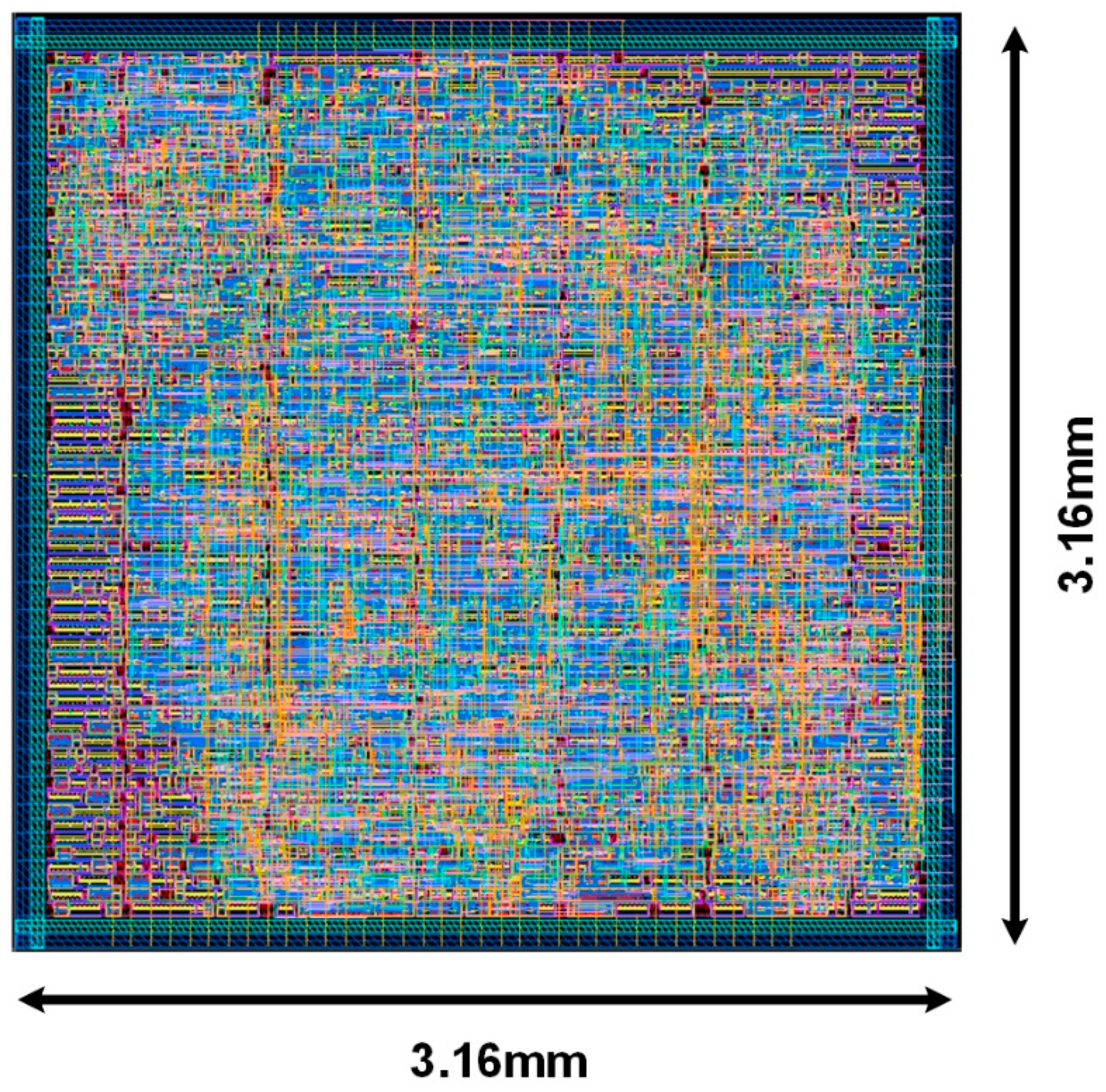
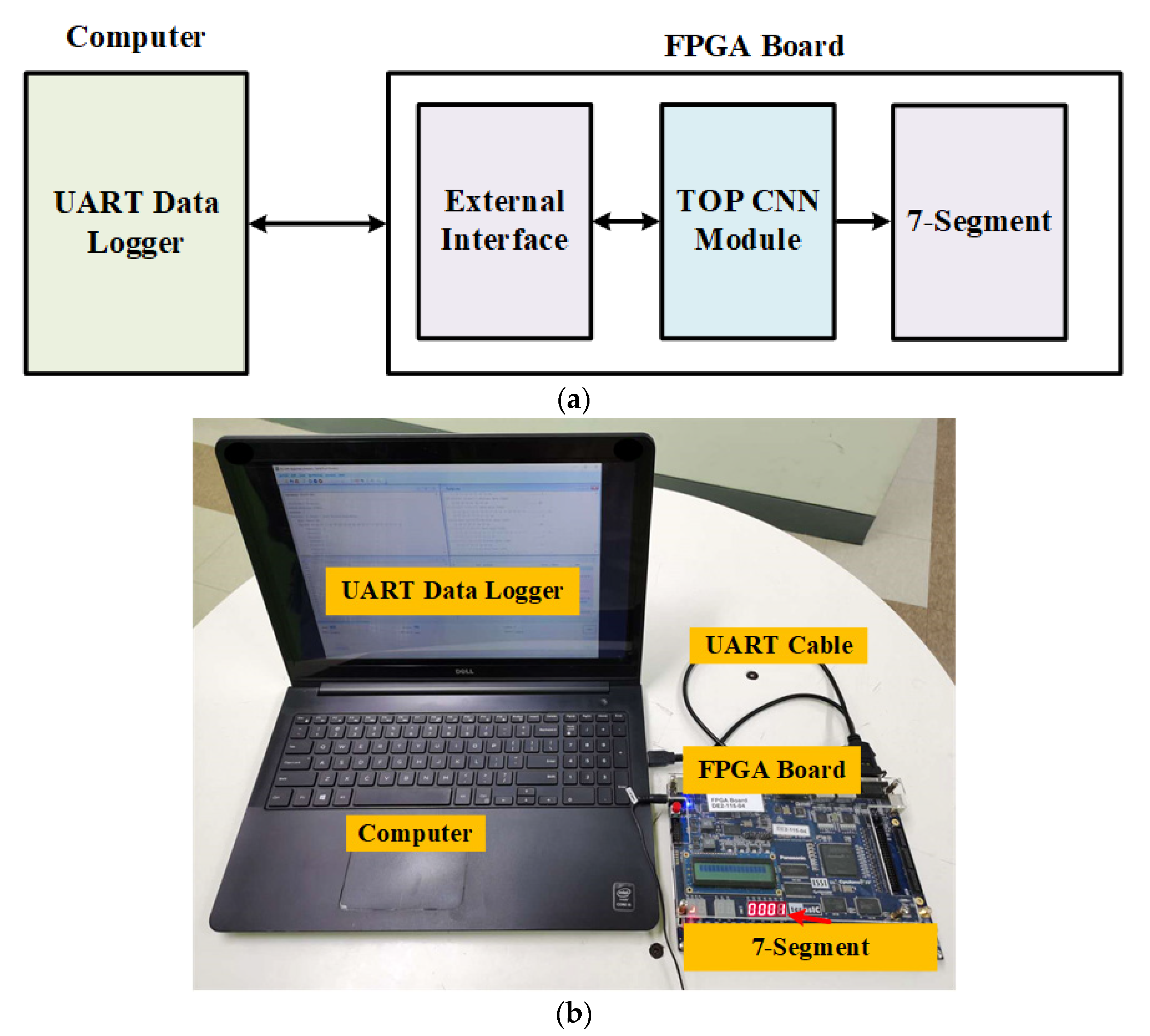
4.2. FPGA Implementation
5. Conclusions
Author Contributions
Funding
Institutional Review Board Statement
Informed Consent Statement
Data Availability Statement
Conflicts of Interest
References
- Justino, C.I.L.; Duarte, A.C.; Rocha-Santos, T.A.P. Recent progress in biosensors for environmental monitoring: A review. Sensors 2017, 17, 2918. [Google Scholar] [CrossRef]
- Schackart, K.E., III; Yoon, J.-Y. Machine Learning Enhances the Performance of Bioreceptor-Free Biosensors. Sensors 2021, 21, 5519. [Google Scholar] [CrossRef]
- Cui, F.; Yue, Y.; Zhang, Y.; Zhang, Z.; Zhou, H.S. Advancing biosensors with machine learning. ACS Sens. 2020, 5, 3346–3364. [Google Scholar] [CrossRef]
- Nguyen, N.; Tran, V.; Ngo, D.; Phan, D.; Lumbanraja, F.; Faisal, M.; Abapihi, B.; Kubo, M.; Satou, K. DNA Sequence Classification by Convolutional Neural Network. J. Biomed. Sci. Eng. 2016, 9, 280–286. [Google Scholar] [CrossRef]
- Jin, X.; Liu, C.; Xu, T.; Su, L.; Zhang, X. Artificial intelligence biosensors: Challenges and prospects. Biosens. Bioelectron. 2020, 165, 112412. [Google Scholar] [CrossRef] [PubMed]
- Shawahna, A.; Sait, S.M.; El-Maleh, A. FPGA-based accelerators of deep learning networks for learning and classification: A review. IEEE Access 2019, 7, 7823–7859. [Google Scholar] [CrossRef]
- Farrukh, F.U.D.; Xie, T.; Zhang, C.; Wang, Z. Optimization for efficient hardware implementation of CNN on FPGA. In Proceedings of the 2018 IEEE International Conference on Integrated Circuits, Technologies and Applications (ICTA), Beijing, China, 21–23 November 2018; pp. 88–89. [Google Scholar]
- Ma, Y.; Cao, Y.; Vrudhula, S.; Seo, J. Optimizing the Convolution Operation to Accelerate Deep Neural Networks on FPGA. IEEE Trans. Very Large Scale Integr. (VLSI) Syst. 2018, 26, 1354–1367. [Google Scholar] [CrossRef]
- Guo, K.; Zeng, S.; Yu, J.; Wang, Y.; Yang, H. A survey of FPGA-based neural network interface accelerator. ACM Trans. Reconfig. Technol. Syst. 2018, 12, 2. [Google Scholar]
- Jiang, Z.; Yin, S.; Seo, J.S.; Seok, M. C3SRAM: An in-memory-computing SRAM macro based on robust capacitive coupling computing mechanism. IEEE J. Solid-State Circuits 2020, 55, 1888–1897. [Google Scholar] [CrossRef]
- Ding, C.; Ren, A.; Yuan, G.; Ma, X.; Li, J.; Liu, N.; Yuan, B.; Wang, Y. Structured Weight Matrices-Based Hardware Accelerators in Deep Neural Networks: FPGAs and ASICs. arXiv 2018, arXiv:1804.11239. [Google Scholar]
- Kim, H.; Choi, K. Low Power FPGA-SoC Design Techniques for CNN-based Object Detection Accelerator. In Proceedings of the 2019 IEEE Annual Ubiquitous Computing, Electronics & Mobile Communication Conference, New York, NY, USA, 10–12 October 2019. [Google Scholar]
- Mujawar, S.; Kiran, D.; Ramasangu, H. An Efficient CNN Architecture for Image Classification on FPGA Accelerator. In Proceedings of the 2018 Second International Conference on Advances in Electronics, Computers and Communications, Bangalore, India, 9–10 February 2018; pp. 1–4. [Google Scholar]
- Ghaffari, A.; Savaria, Y. CNN2Gate: An Implementation of Convolutional Neural Networks Inference on FPGAs with Automated Design Space Exploration. Electronics 2020, 9, 2200. [Google Scholar] [CrossRef]
- Kang, M.; Lee, Y.; Park, M. Energy Efficiency of Machine Learning in Embedded Systems Using Neuromorphic Hardware. Electronics 2020, 9, 1069. [Google Scholar] [CrossRef]
- Schuman, C.D.; Potok, T.E.; Patton, R.M.; Birdwell, J.D.; Dean, M.E.; Rose, G.S.; Plank, J.S. A Survey of Neuromorphic Computing and Neural Networks in Hardware. arXiv 2017, arXiv:1705.06963. [Google Scholar]
- Liu, B.; Li, H.; Chen, Y.; Li, X.; Wu, Q.; Huang, T. Vortex: Variation-aware training for memristor X-bar. In Proceedings of the 52nd Annual Design Automation Conference, San Francisco, CA, USA, 8–12 June 2015; pp. 1–6. [Google Scholar]
- Chang, J.; Sha, J. An Efficient Implementation of 2D convolution in CNN. IEICE Electron. Express 2017, 14, 20161134. [Google Scholar] [CrossRef]
- Marukame, T.; Nomura, K.; Matusmoto, M.; Takaya, S.; Nishi, Y. Proposal analysis and demonstration of Analog/Digital-mixed Neural Networks based on memristive device arrays. In Proceedings of the 2018 IEEE International Symposium on Circuits and Systems (ISCAS), Florence, Italy, 27–30 May 2018; pp. 1–5. [Google Scholar]
- Bankman, D.; Yang, L.; Moons, B.; Verhelst, M.; Murmann, B. An Always-On 3.8 μJ/86% CIFAR-10 Mixed-Signal Binary CNN Processor with All Memory on Chip in 28 nm CMOS. IEEE J. Solid-State Circuits 2018, 54, 158–172. [Google Scholar] [CrossRef]
- Indiveri, G.; Corradi, F.; Qiao, N. Neuromorphic Architectures for Spiking Deep Neural Networks. In Proceedings of the 2015 IEEE International Electron Devices Meeting (IEDM), Washington, DC, USA, 7–9 December 2015; pp. 421–424. [Google Scholar]
- Chen, P.; Gao, L.; Yu, S. Design of Resistive Synaptic Array for Implementing On-Chip Sparse Learning. IEEE Trans. Multi-Scale Comput. Syst. 2016, 2, 257–264. [Google Scholar] [CrossRef]
- Hardware Acceleration of Deep Neural Networks: GPU, FPGA, ASIC, TPU, VPU, IPU, DPU, NPU, RPU, NNP and Other Letters. Available online: https://itnesweb.com/article/hardware-acceleration-of-deep-neural-networks-gpu-fpga-asic-tpu-vpu-ipu-dpu-npu-rpu-nnp-and-other-letters (accessed on 12 March 2020).
- Pedram, M.; Abdollahi, A. Low-power RT-level synthesis techniques: A tutorial. IEE Proc. Comput. Digit. Tech. 2005, 152, 333–343. [Google Scholar] [CrossRef][Green Version]
- Ahn, M.; Hwang, S.J.; Kim, W.; Jung, S.; Lee, Y.; Chung, M.; Lim, W.; Kim, Y. AIX: A high performance and energy efficient inference accelerator on FPGA for a DNN-based commercial speech recognition. In Proceedings of the 2019 Design, Automation & Test in Europe Conference & Exhibition (DATE), Florence, Italy, 25–29 March 2019; pp. 1495–1500. [Google Scholar]
- Krestinskaya, O.; James, A.P. Binary Weighted Memristive Analog Deep Neural Network for Near-Sensor Edge Processing. In Proceedings of the 2018 IEEE 18th International Conference on Nanotechnology (IEEE-NANO), Cork, Ireland, 23–26 July 2018; pp. 1–4. [Google Scholar]
- Hasan, R.; Taha, T.M. Enabling Back Propagation Training of Memristor Crossbar Neuromorphic Processors. In Proceedings of the 2014 International Joint Conference on Neural Networks (IJCNN), Beijing, China, 6–11 July 2014; pp. 21–28. [Google Scholar]
- Zhang, C.; Li, P.; Sun, G.; Guan, Y.; Xiao, B.; Cong, J. Optimizing fpga-based accelerator design for deep convolutional neural networks. In Proceedings of the 2015 ACM/SIGDA International Symposium on Field-Programmable Gate Arrays, Monterey, CA, USA, 22–24 February 2015; pp. 161–170. [Google Scholar]
- Yann, L. The MNIST Database of Handwritten Digits. 1998. Available online: http://yann.lecun.com/exdb/mnist/ (accessed on 1 January 2022).


| Parameter | This Work | [17] | [12] | [16] |
|---|---|---|---|---|
| Process (nm) | CMOS 28 | CMOS 28 | CMOS 65 | CMOS 40 |
| Architecture | Digital | Digital and Analog | Digital | Digital and Analog |
| Design Entry | RTL | - | RTL | - |
| Frequency (MHz) | 100 | 300 | 550 | 204 |
| CNN Model | 6 layers | 11 layers | 9 layers (CNN/MLP) | - |
| Datasets | MNIST | CIFAR-10 | MNIST | MNIST |
| V (V) | 1.8 | 0.8 | 1 | 0.55–1.1 |
| Power(W) | 2.93 | 0.000899 | 0.00012 | 25 |
| Accuracy (%) | 92 | 86.05 | 98 | 98.2 |
| On-Chip Memory | 10 Kb | 2676 Kb | - | - |
| Off-Chip Memory | 40 Kb | no | - | - |
| Throughput (FPS) | 5.33 k | - | 8.6 M | 1 k |
| Chip Area (mm2) | 9.986 | 5.76 | 15 | - |
Publisher’s Note: MDPI stays neutral with regard to jurisdictional claims in published maps and institutional affiliations. |
© 2022 by the authors. Licensee MDPI, Basel, Switzerland. This article is an open access article distributed under the terms and conditions of the Creative Commons Attribution (CC BY) license (https://creativecommons.org/licenses/by/4.0/).
Share and Cite
Kumar, P.; Yingge, H.; Ali, I.; Pu, Y.-G.; Hwang, K.-C.; Yang, Y.; Jung, Y.-J.; Huh, H.-K.; Kim, S.-K.; Yoo, J.-M.; et al. A Configurable and Fully Synthesizable RTL-Based Convolutional Neural Network for Biosensor Applications. Sensors 2022, 22, 2459. https://doi.org/10.3390/s22072459
Kumar P, Yingge H, Ali I, Pu Y-G, Hwang K-C, Yang Y, Jung Y-J, Huh H-K, Kim S-K, Yoo J-M, et al. A Configurable and Fully Synthesizable RTL-Based Convolutional Neural Network for Biosensor Applications. Sensors. 2022; 22(7):2459. https://doi.org/10.3390/s22072459
Chicago/Turabian StyleKumar, Pervesh, Huo Yingge, Imran Ali, Young-Gun Pu, Keum-Cheol Hwang, Youngoo Yang, Yeon-Jae Jung, Hyung-Ki Huh, Seok-Kee Kim, Joon-Mo Yoo, and et al. 2022. "A Configurable and Fully Synthesizable RTL-Based Convolutional Neural Network for Biosensor Applications" Sensors 22, no. 7: 2459. https://doi.org/10.3390/s22072459
APA StyleKumar, P., Yingge, H., Ali, I., Pu, Y.-G., Hwang, K.-C., Yang, Y., Jung, Y.-J., Huh, H.-K., Kim, S.-K., Yoo, J.-M., & Lee, K.-Y. (2022). A Configurable and Fully Synthesizable RTL-Based Convolutional Neural Network for Biosensor Applications. Sensors, 22(7), 2459. https://doi.org/10.3390/s22072459