
Analytical and Experimental Performance Analysis of Enhanced Wake-Up Receivers Based on Low-Power Base-Band Amplifiers


Abstract
:1. Introduction
2. Related Works
3. Analytical Expressions
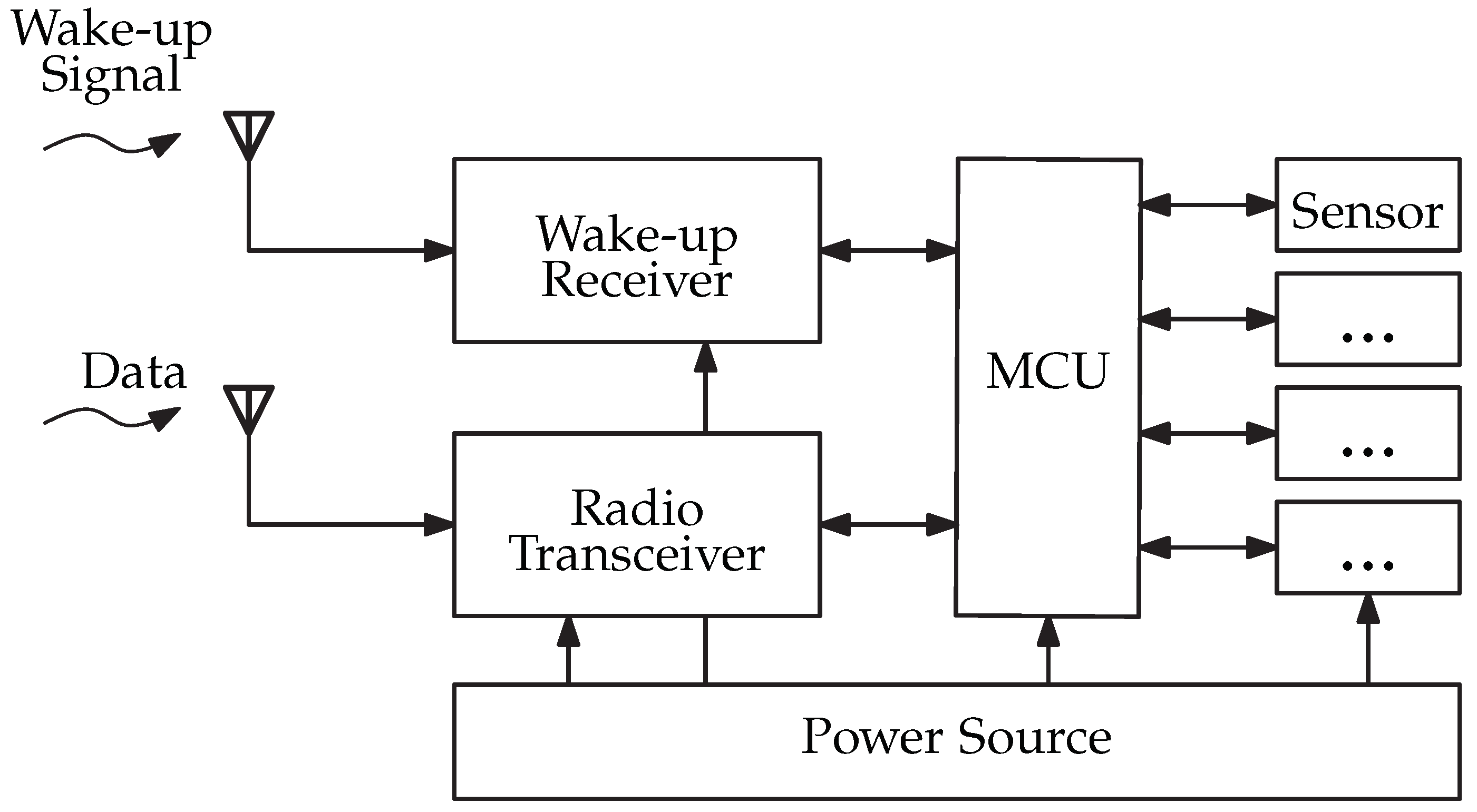
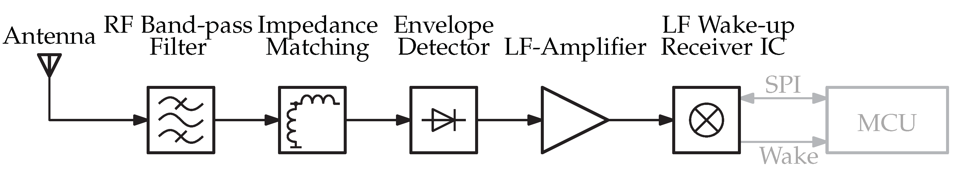
3.1. General Structure of the Adopted WuRx Circuit
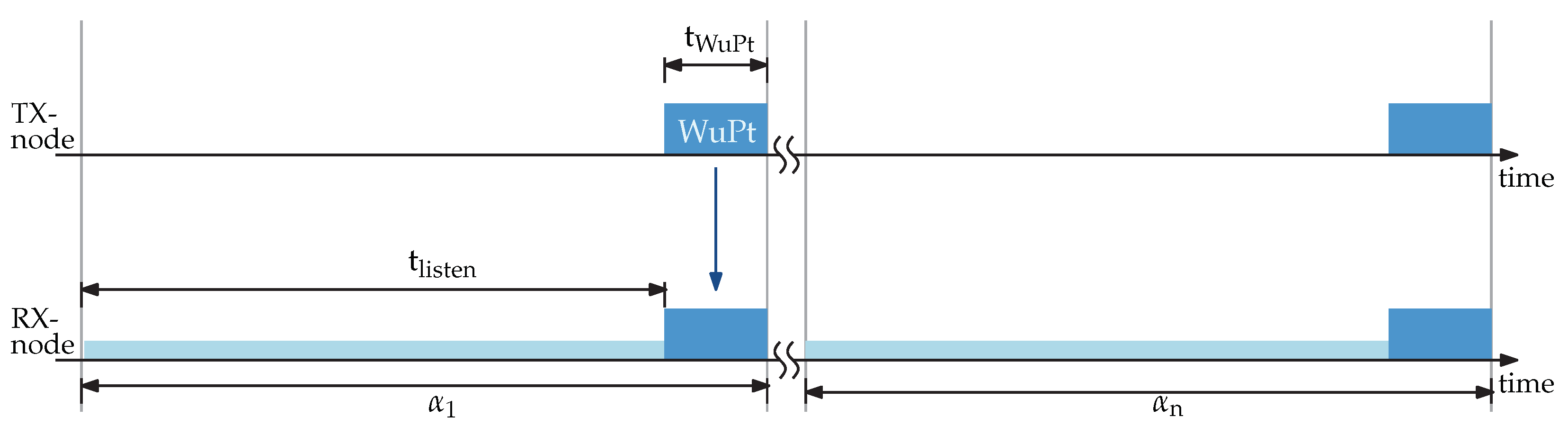
3.2. Energy Consumption
3.3. Path and Antenna Losses
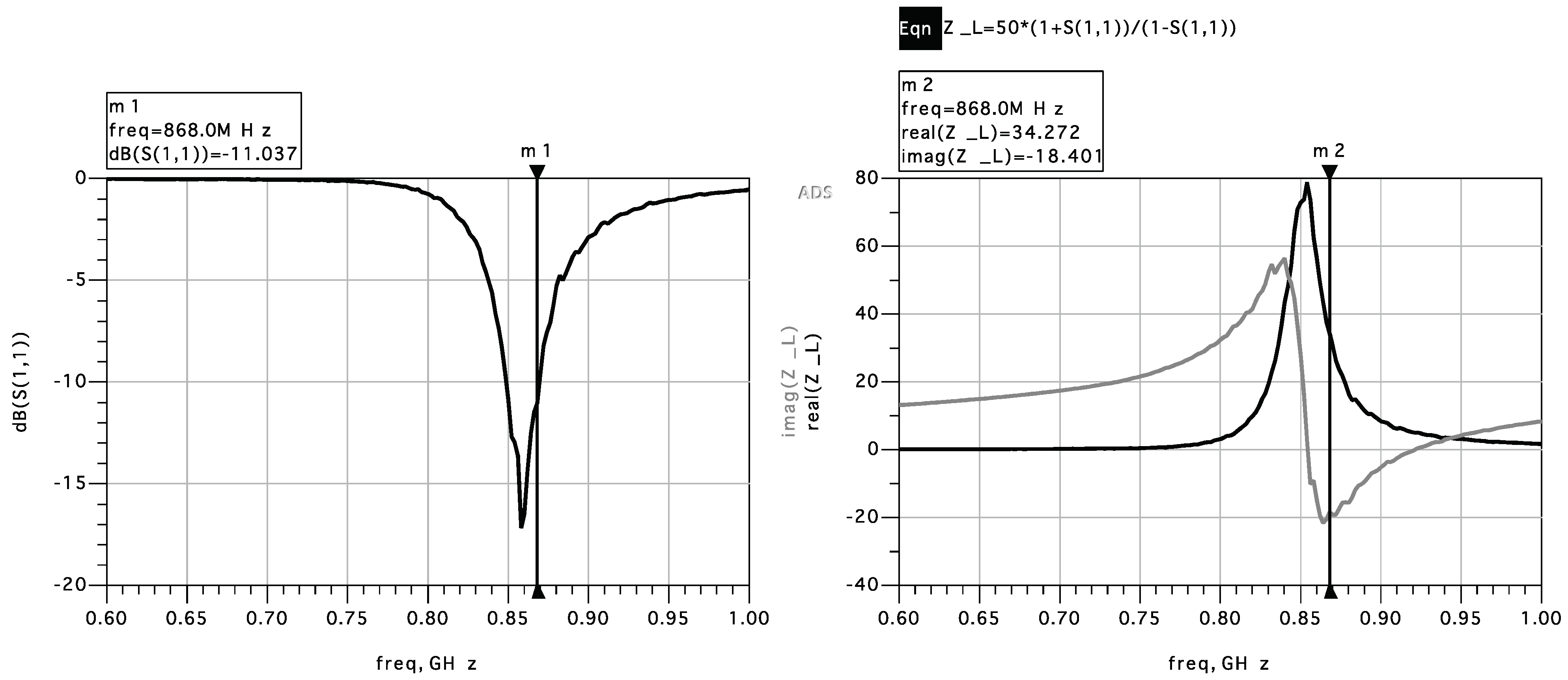
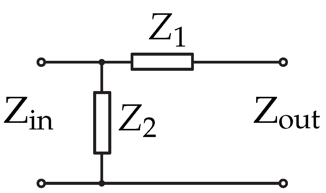
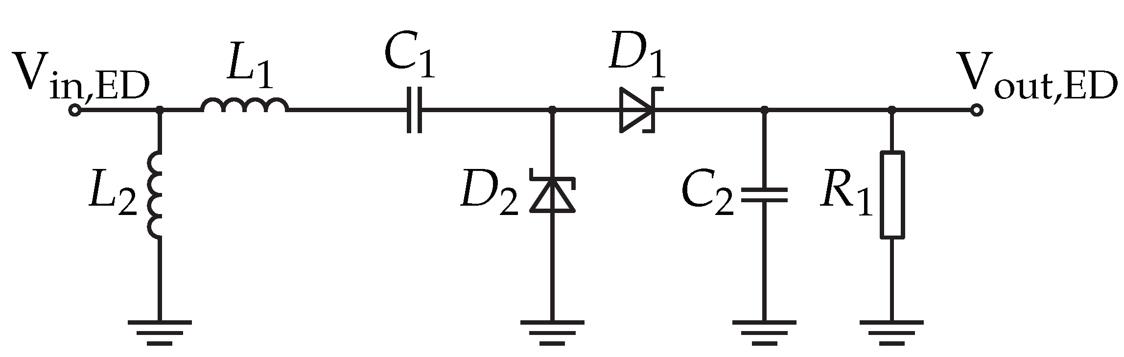
3.4. Impedance Matching and Envelope Detector
3.5. Low-Frequency Amplifiers
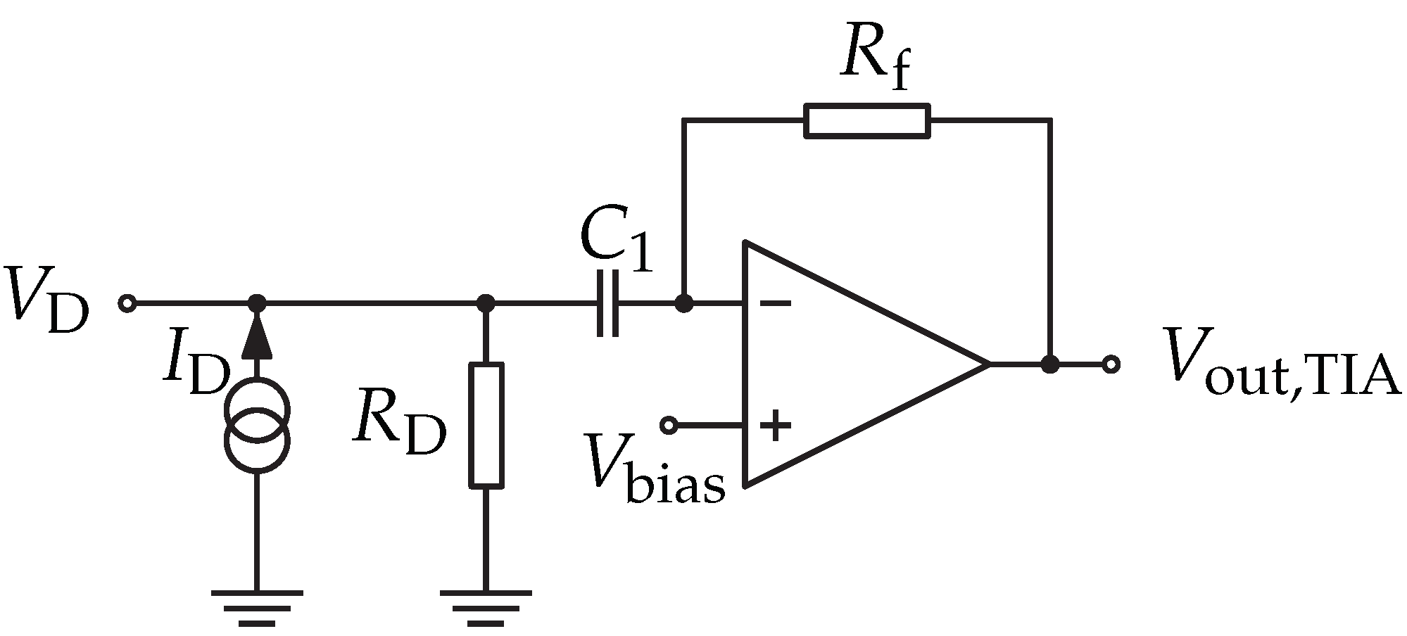
3.5.1. Transimpedance Amplifier (TIA)
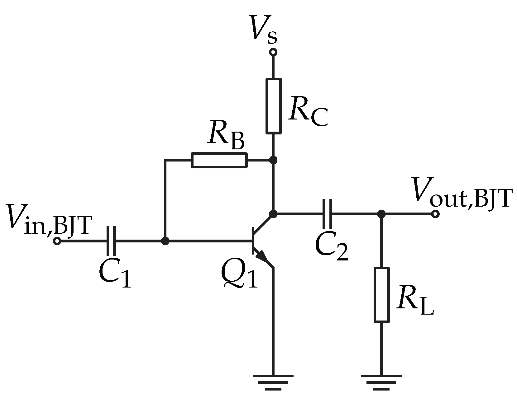
3.5.2. BJT-Based Amplifier Circuit
3.6. Low-Frequency Wake-Up Chip
4. Investigation Results
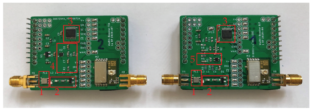
4.1. Overall System
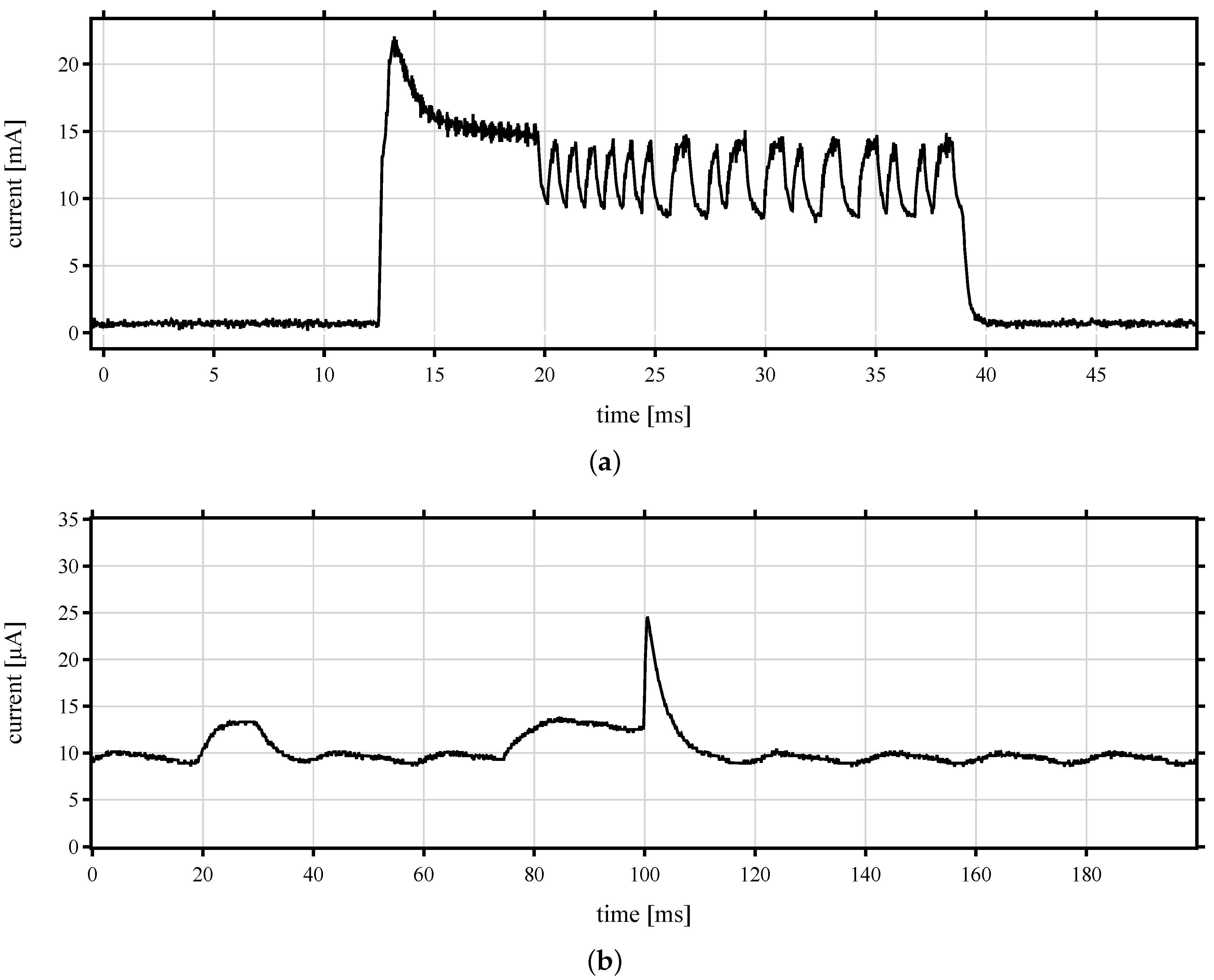
4.2. Energy Consumption
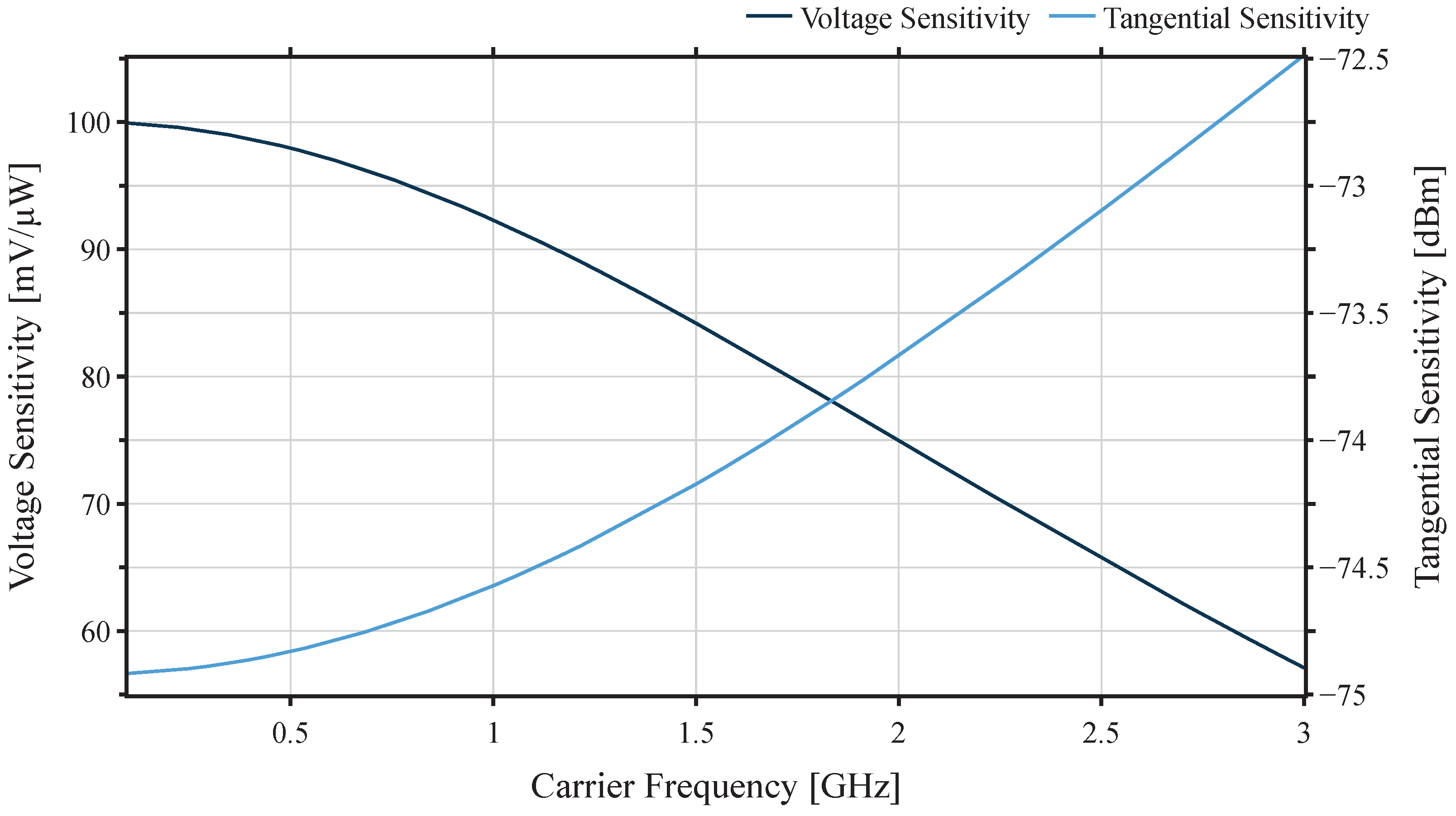
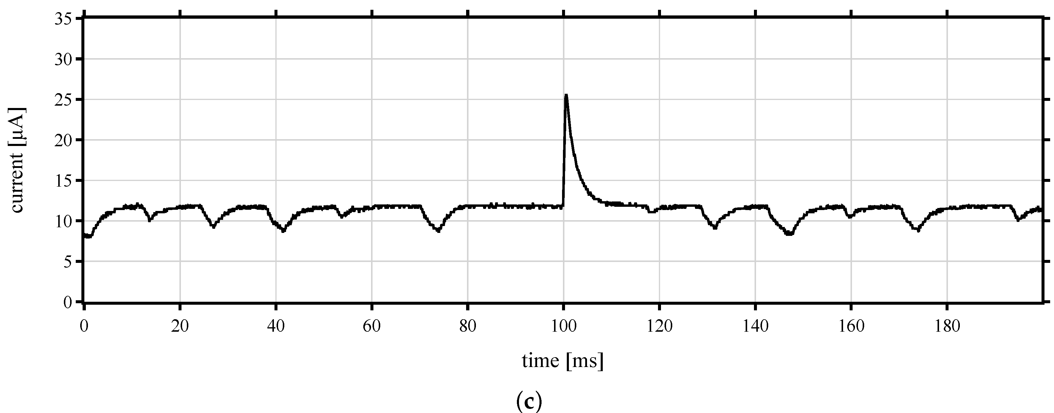
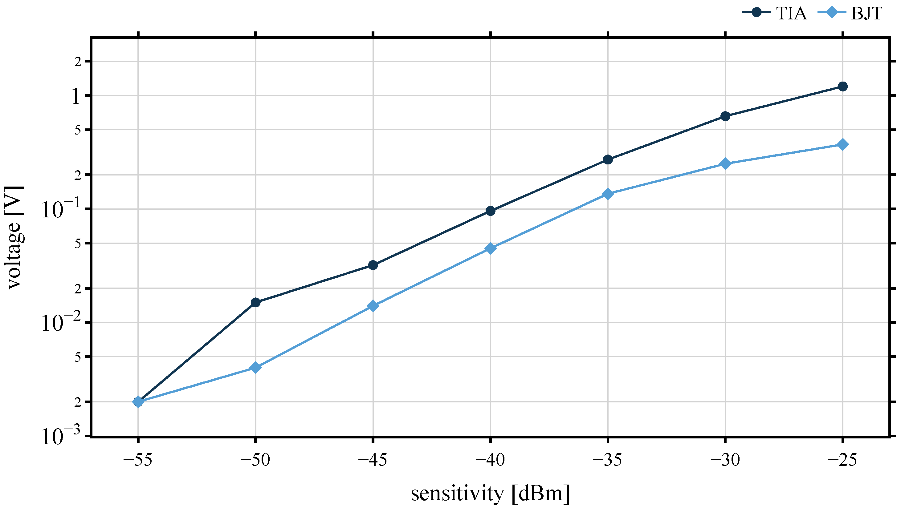
4.3. Sensitivity Measurements
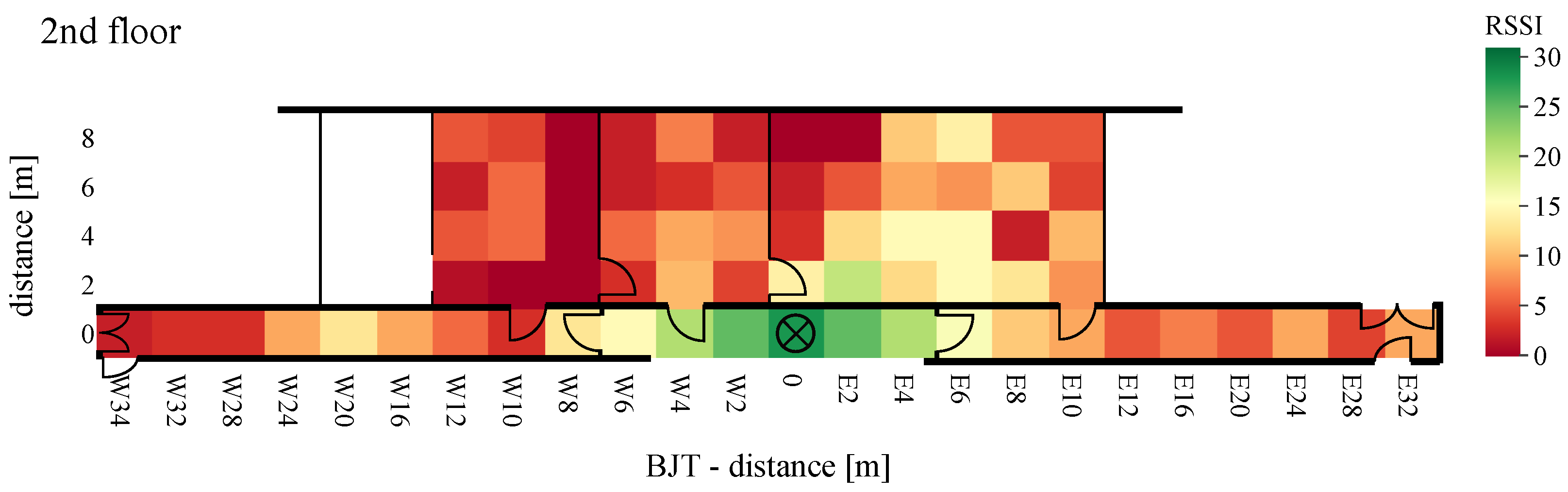
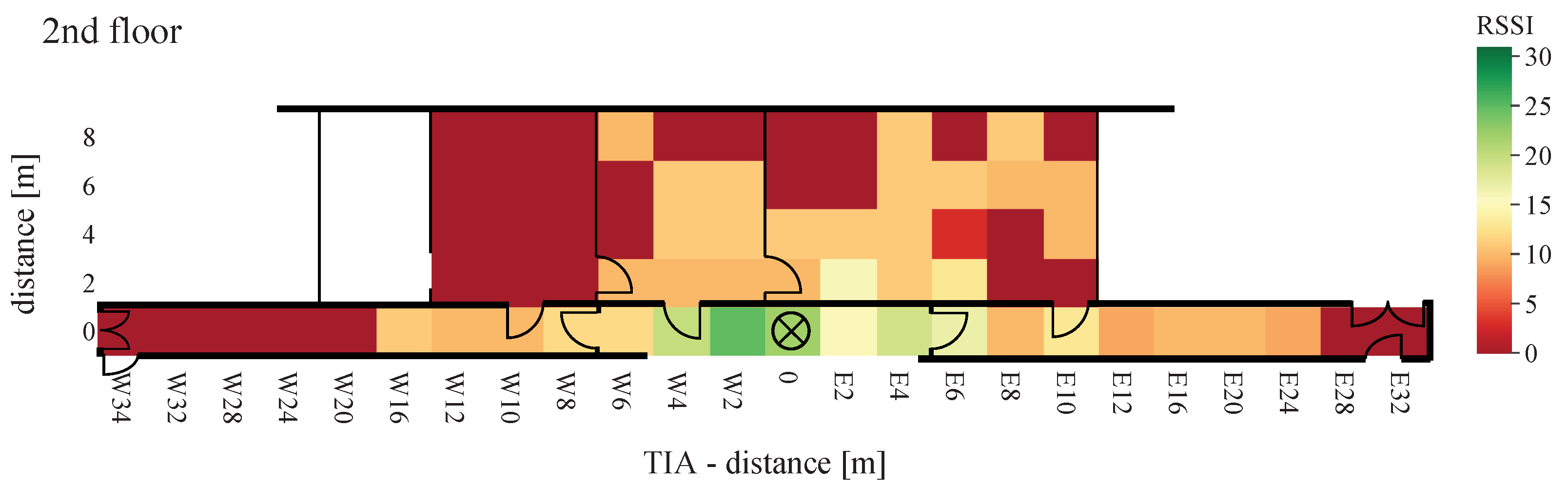
4.4. Indoor Operational Range Evaluations
5. Conclusions
Author Contributions
Funding
Acknowledgments
Conflicts of Interest
Abbreviations
| AGC | automatic gain control |
| ASK | amplitude shift keying |
| BJT | bipolar junction transistor |
| CMOS | complementary metal-oxide semiconductor |
| COTS | commercial of the shelf |
| FSK | frequency shift keying |
| GBWP | gain bandwidth product |
| IoT | Internet of Things |
| ITU | International Telecommunication Union |
| LED | light-emitting diode |
| LF | low frequency |
| LNA | low noise amplifier |
| MCU | main microcontroller unit |
| OA | operational amplifier |
| OOK | on-off-keying |
| PCB | printed circuit board |
| PER | package error rate |
| RF | radio frequency |
| RSSI | received signal strength indicator |
| SAW | surface acoustic wave |
| SoA | State of the Art |
| TIA | transimpedance amplifier |
| TSS | tangential signal sensitivity |
| VGA | variable gain amplifier |
| WSN | wireless sensor network |
| WuPt | wake-up packet |
| WuRx | wake-up receiver |
| WuTx | wake-up transmitter |
References
- Khriji, S.; Houssaini, D.E.; Kammoun, I.; Besbes, K.; Kanoun, O. Energy-Efficient Routing Algorithm Based on Localization and Clustering Techniques for Agricultural Applications. IEEE Aerosp. Electron. Syst. Mag. 2019, 34, 56–66. [Google Scholar] [CrossRef]
- Da Costa, E.F.; de Oliveira, N.E.; Morais, F.J.O.; Carvalhaes-Dias, P.; Duarte, L.F.C.; Cabot, A.; Siqueira Dias, J.A. A Self-Powered and Autonomous Fringing Field Capacitive Sensor Integrated into a Micro Sprinkler Spinner to Measure Soil Water Content. Sensors 2017, 17, 575. [Google Scholar] [CrossRef] [Green Version]
- Ben Dhaou, I.; Ebrahimi, M.; Ben Ammar, M.; Bouattour, G.; Kanoun, O. Edge Devices for Internet of Medical Things: Technologies, Techniques, and Implementation. Electronics 2021, 10, 2104. [Google Scholar] [CrossRef]
- Al-Ali, A.; Aji, Y.; Othman, H.; Fakhreddin, F. Wireless smart sensors networks overview. In Proceedings of the Second IFIP International Conference on Wireless and Optical Communications Networks, 2005. WOCN 2005, Dubai, United Arab Emirates, 6–8 March 2005; pp. 536–540. [Google Scholar] [CrossRef]
- Rawat, P.; Singh, K.D.; Chaouchi, H.; Bonnin, J.M. Wireless sensor networks: A survey on recent developments and potential synergies. J. Supercomput. 2014, 68, 1–48. [Google Scholar] [CrossRef]
- Willig, A. Wireless sensor networks: Concept, challenges and approaches. e & i Elektrotechnik und Informationstechnik 2006, 123, 224–231. [Google Scholar] [CrossRef]
- Kanoun, O.; Bradai, S.; Khriji, S.; Bouattour, G.; El Houssaini, D.; Ben Ammar, M.; Naifar, S.; Bouhamed, A.; Derbel, F.; Viehweger, C. Energy-Aware System Design for Autonomous Wireless Sensor Nodes: A Comprehensive Review. Sensors 2021, 21, 548. [Google Scholar] [CrossRef]
- Peruzzi, G.; Pozzebon, A. A Review of Energy Harvesting Techniques for Low Power Wide Area Networks (LPWANs). Energies 2020, 13, 3433. [Google Scholar] [CrossRef]
- Bouattour, G.; Hu, Z.; Jmeaa Derbel, H.B.; Kanoun, O. Smart Multi-coil Inductive Power Tranmission with IoT Based Visulization. In Proceedings of the 2020 IEEE 6th World Forum on Internet of Things (WF-IoT), New Orleans, LA, USA, 2–16 June 2020; pp. 1–6. [Google Scholar] [CrossRef]
- Schneider, E.; Derbel, F.; Strakosch, F. Energy harvesting and management of continuously powered WSNs. In Proceedings of the 2017 14th International Multi-Conference on Systems, Signals & Devices (SSD), Marrakech, Morocco, 28–31 March 2017; pp. 347–353. [Google Scholar] [CrossRef]
- Abo-Zahhad, M.; Farrag, M.; Ali, A. Optimization of Transmitted Power and Modulation Level for Minimizing Energy Consumption in Wireless Sensor Networks. Wirel. Pers. Commun. 2017, 96, 4047–4062. [Google Scholar] [CrossRef]
- Caballe, M.C.; Auge, A.C.; Aspas, J.P. Wake-Up Radio: An Enabler of Wireless Convergence. IEEE Access 2021, 9, 3784–3797. [Google Scholar] [CrossRef]
- Del-Valle-Soto, C.; Mex-Perera, C.; Nolazco-Flores, J.A.; Velázquez, R.; Rossa-Sierra, A. Wireless Sensor Network Energy Model and Its Use in the Optimization of Routing Protocols. Energies 2020, 13, 728. [Google Scholar] [CrossRef] [Green Version]
- Bhatt, M.; Boddapati, H.K.; Prakriya, S. Performance off cluster-based multi-hop underlay networks with energy harvesting nodes. IET Commun. 2020, 14, 1476–1484. [Google Scholar] [CrossRef]
- Ye, W.; Heidemann, J.; Estrin, D. An energy-efficient MAC protocol for wireless sensor networks. In Proceedings of the Twenty-First Annual Joint Conference of the IEEE Computer and Communications Societies, New York, NY, USA, 23–27 June 2002; Volume 3, pp. 1567–1576. [Google Scholar] [CrossRef]
- Durante, M.S.; Mahlknecht, S. An Ultra Low Power Wakeup Receiver for Wireless Sensor Nodes. In Proceedings of the 2009 Third International Conference on Sensor Technologies and Applications, Athens, Greece, 18–23 June 2009; pp. 167–170. [Google Scholar] [CrossRef]
- Polastre, J.; Hill, J.; Culler, D. Versatile low power media access for wireless sensor networks. In Proceedings of the 2nd International Conference on Embedded Networked Sensor Systems, Baltimore, MD, USA, 3–5 November 2004; p. 95. [Google Scholar] [CrossRef]
- Whichi, A.; Weber, M.; Ketata, I.; Sahnoun, S.; Derbel, F. Simulation of Wireless Sensor Nodes based on Wake-Up Receivers. In Proceedings of the 2021 18th International Multi-Conference on Systems, Signals Devices (SSD), Monastir, Tunisia, 22–25 March 2021; pp. 235–240. [Google Scholar] [CrossRef]
- Magno, M.; Marinkovic, S.; Srbinovski, B.; Popovici, E.M. Wake-up radio receiver based power minimization techniques for wireless sensor networks: A review. Microelectron. J. 2014, 45, 1627–1633. [Google Scholar] [CrossRef]
- Kozłowski, A.; Sosnowski, J. Energy Efficiency Trade-Off Between Duty-Cycling and Wake-Up Radio Techniques in IoT Networks. Wirel. Pers. Commun. 2019, 107, 1951–1971. [Google Scholar] [CrossRef] [Green Version]
- Moody, J.; Bassirian, P.; Roy, A.; Liu, N.; Barker, N.S.; Calhoun, B.H.; Bowers, S.M. Interference Robust Detector-First Near-Zero Power Wake-Up Receiver. IEEE J. Solid-State Circuits 2019, 54, 2149–2162. [Google Scholar] [CrossRef]
- Elgani, A.; Magno, M.; Renzini, F.; Perilli, L.; Scarselli, E.F.; Gnudi, A.; Canegallo, R.; Ricotti, G.; Benini, L. Nanowatt Wake-Up Radios: Discrete-Components and Integrated Architectures. In Proceedings of the 2018 25th IEEE International Conference on Electronics, Circuits and Systems (ICECS), Bordeaux, France, 9–12 December 2018. [Google Scholar] [CrossRef]
- Zgaren, M.; Sawan, M. A high-sensitivity battery-less wake-up receiver for 915 MHz ISM band applications. In Proceedings of the 2015 IEEE International Conference on Electronics, Circuits and Systems, Cairo, Egypt, 6–9 December 2015; pp. 336–339. [Google Scholar] [CrossRef]
- Piyare, R.; Murphy, A.L.; Kiraly, C.; Tosato, P.; Brunelli, D. Ultra Low Power Wake-Up Radios: A Hardware and Networking Survey. IEEE Commun. Surv. Tutor. 2017, 19, 2117–2157. [Google Scholar] [CrossRef]
- Oller, J.; Demirkol, I.; Casademont, J.; Paradells, J.; Gamm, G.U.; Reindl, L. Performance evaluation and comparative analysis of SubCarrier Modulation Wake-up Radio systems for energy-efficient wireless sensor networks. Sensors 2013, 14, 22–51. [Google Scholar] [CrossRef] [PubMed] [Green Version]
- Basagni, S.; Ceccarelli, F.; Petrioli, C.; Raman, N.; Sheshashayee, A.V. Wake-up Radio Ranges: A Performance Study. In Proceedings of the 2019 IEEE Wireless Communications and Networking Conference (WCNC), Marrakesh, Morocco, 15–18 April 2019; pp. 1–6. [Google Scholar] [CrossRef]
- Marinkovic, S.J.; Popovici, E.M. Nano-Power Wireless Wake-Up Receiver With Serial Peripheral Interface. IEEE J. Sel. Areas Commun. 2011, 29, 1641–1647. [Google Scholar] [CrossRef]
- Magno, M.; Jelicic, V.; Srbinovski, B.; Bilas, V.; Popovici, E.; Benini, L. Design, Implementation, and Performance Evaluation of a Flexible Low-Latency Nanowatt Wake-Up Radio Receiver. IEEE Trans. Ind. Inform. 2016, 12, 633–644. [Google Scholar] [CrossRef]
- Pflaum, F.; Weigel, R.; Koelpin, A. Ultra-low-power sensor node with wake-up-functionality for smart-sensor-applications. In Proceedings of the 2018 IEEE Topical Conference on Wireless Sensors and Sensor Networks (WiSNet), Anaheim, CA, USA, 14–17 January 2018; pp. 107–110. [Google Scholar] [CrossRef]
- Bdiri, S.; Derbel, F.; Kanoun, O. A Tuned-RF Duty-Cycled Wake-Up Receiver with -90 dBm Sensitivity. Sensors 2017, 18, 86. [Google Scholar] [CrossRef] [PubMed] [Green Version]
- Kazdaridis, G.; Sidiropoulos, N.; Zografopoulos, I.; Korakis, T. eWake: A Novel Architecture for Semi-Active Wake-Up Radios Attaining Ultra-High Sensitivity at Extremely-Low Consumption. arXiv 2021, arXiv:cs.AR/2103.15969. [Google Scholar]
- Koeble, S.; Heller, S.; Woias, P. A narrow-band and ultra-low-power 433 MHz wake-up receiver. J. Phys. Conf. Ser. 2019, 1407, 012093. [Google Scholar] [CrossRef]
- Woias, P.; Heller, S.; Pelz, U. A highly sensitive and ultra-low-power wake-up receiver for energy-autonomous embedded systems. J. Phys. Conf. Ser. 2018, 1052, 012024. [Google Scholar] [CrossRef]
- Gamm, G.U.; Sippel, M.; Kostic, M.; Reindl, L.M. Low power wake-up receiver for wireless sensor nodes. In Proceedings of the Sixth International Conference on Intelligent Sensors, Sensor Networks, and Information Processing (ISSNIP), Brisbane, Australia, 7–10 December 2010; pp. 121–126. [Google Scholar] [CrossRef]
- Bdiri, S.; Derbel, F. A nanowatt Wake-Up Receiver for industrial production line. In Proceedings of the 2014 IEEE 11th International Multi-Conference on Systems, Signals & Devices (SSD14), Barcelona, Spain, 11–14 February 2014; pp. 1–6. [Google Scholar] [CrossRef]
- Ammar, Y.; Bdiri, S.; Derbel, F. An ultra-low power wake up receiver with flip flops based address decoder. In Proceedings of the 2015 IEEE 12th International Multi-Conference on Systems, Signals & Devices (SSD15), Mahdia, Tunisia, 16–19 March 2015; pp. 1–5. [Google Scholar] [CrossRef]
- Froytlog, A.; Cenkeramaddi, L.R. Design and Implementation of an Ultra-Low Power Wake-up Radio for Wireless IoT Devices. In Proceedings of the 2018 IEEE International Conference on Advanced Networks and Telecommunications Systems (ANTS), Indore, India, 16–19 December 2018; pp. 1–4. [Google Scholar] [CrossRef]
- Fromm, R.; Schott, L.; Derbel, F. An Efficient Low-power Wake-up Receiver Architecture for Power Saving for Transmitter and Receiver Communications. In Proceedings of the 10th International Conference on Sensor Networks (SENSORNETS 2021), Online, 9–10 February 2021; pp. 61–68. [Google Scholar] [CrossRef]
- Friis, H.T. A Note on a Simple Transmission Formula. Proc. IRE 1946, 34, 254–256. [Google Scholar] [CrossRef]
- International Telecommunication Union. Propagation Data and Prediction Methods for the Planning of Indoor Radiocommunication Systems and Radio Local Area Networks in the Frequency Range 300 MHz to 450 GHz; International Telecommunication Union: Geneva, Switzerland, 2021. [Google Scholar]
- Tran, L.G.; Cha, H.K.; Park, W.T. RF power harvesting: A review on designing methodologies and applications. Micro Nano Syst. Lett. 2017, 5, 14. [Google Scholar] [CrossRef] [Green Version]
- Bahl, I.J.; Bhartia, P. Microwave Solid State Circuit Design, 2nd ed.; Wiley-Interscience: Hoboken, NJ, USA, 2003. [Google Scholar]
- Hewlett-Packard Co. Schottky Barrier Diode Video Detectors: Application Note 923; Hewlett-Packard Co.: Palo Alto, CA, USA, 1986. [Google Scholar]
- Ams AG. AS3933: Datasheet: 3D Low Frequency Wake-up Receiver; Ams AG: Premstatten, Austria, 2015. [Google Scholar]
- Tietze, U.; Schenk, C.; Gamm, E. Halbleiter-Schaltungstechnik, 15th ed.; Springer: Berlin/Heidelberg, Germany, 2016. [Google Scholar]
- Ams AG. Application Note AS3933 RSSI to Voltage Conversion; Ams AG: Premstatten, Austria, 2014. [Google Scholar]
- Micrel Inc. MIC861—Ultra-Low-Power Op Amp; Micrel Inc.: San Jose, CA, USA, 2014. [Google Scholar]
- Mc Caffrey, C.; Sillanpaa, T.; Huovila, H.; Nikunen, J.; Hakulinen, S.; Pursula, P. Energy Autonomous Wireless Valve Leakage Monitoring System With Acoustic Emission Sensor. IEEE Trans. Circuits Syst. I Regul. Pap. 2017, 64, 2884–2893. [Google Scholar] [CrossRef]


| Reference | [25] | [27] | [29] | [30] | [31] | [32] | [33] | This Work |
|---|---|---|---|---|---|---|---|---|
| Frequency (MHz) | 868 | 868 | 868 | 868 | 868 | 433 | 433 | 868 |
| Sensitivity (dBm) | −53 | −51 | −71 | −90 | −70 | −63 | −63 | −62 |
| Voltage amplification | none | VM | LNA | LNA | OA | BJT | BJT | OA and BJT |
| Listening mode | AO 1 | AO | DC 2 | DC | AO | AO | AO | AO |
| Data rate (kbit/s) | 2.7 | 1.0 | 250 | 128 | 0.04 | 1.0 | 1.0 | 1.2 |
| Current requirement transmitter 3 (μAs) | 148 | 400 | 165 | 803 | 10,000 | 400 | 400 | 345 |
| Components | Parameters | Values |
|---|---|---|
| Antenna ANT-868-CW | Center Frequency | 868 MHz |
| Impedance | 50 Ω | |
| Peak Gain | −2.3 dBi | |
| Bandwidth | 30 MHz | |
| SPIRIT1 SPSGRFC-868 | Supply Current TX Mode | 21 mA |
| Supply Current RX Mode | 9 mA | |
| SAW Filter B39871B | Center Frequency | 869 MHz |
| Maximum Insertion Attenuation | 2.5 dB | |
| Usable Pass band | 2 MHz | |
| Schottky Diodes SMS7630 | Voltage Sensitivity | 40 mV/μ |
| Video Resistance | 5 kΩ | |
| BFP405 NPN RF Bipolar Transistor | Maximum Gain | 23 dB |
| Minimum Noise Figure | 1.25 dB | |
| Collector Current | 1.3 μA | |
| MIC861 Operational Amplifier | Supply Current | 4.2 μA |
| Gain Bandwidth Product | 350 kHz | |
| AS3933 LF Wake-Up-Chip | Supply Current Scanning Mode | 3.1 μA |
| Supply Current Preamble Detection | 12 μA | |
| MSP430 Microcontroller | Supply Current Standby | 860 nA |
| Supply Current Active | 2 mA | |
| System Clock | 8 MHz |
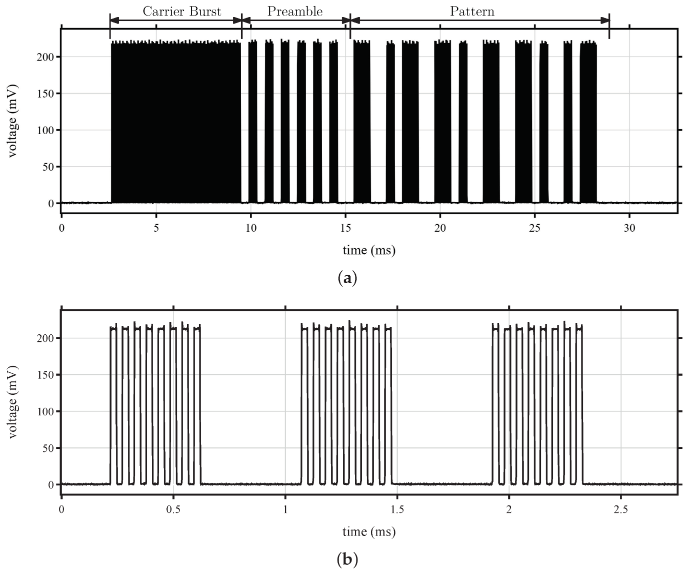
| Segment | Length | Duration (ms) |
|---|---|---|
| Carrier burst | 32 pulses | 8.3 |
| Preamble | 6.5 periods | 5.6 |
| Address | 16 bits | 13.8 |
| Mode | TIA | BJT |
|---|---|---|
| Listening * [μJ] | 28.35 | 25.05 |
| Receiving [μJ] | 1.52 | 1.28 |
| Transmission [mJ] | 1.91 | 1.91 |
Publisher’s Note: MDPI stays neutral with regard to jurisdictional claims in published maps and institutional affiliations. |
© 2022 by the authors. Licensee MDPI, Basel, Switzerland. This article is an open access article distributed under the terms and conditions of the Creative Commons Attribution (CC BY) license (https://creativecommons.org/licenses/by/4.0/).
Share and Cite
Schott, L.; Fromm, R.; Bouattour, G.; Kanoun, O.; Derbel, F. Analytical and Experimental Performance Analysis of Enhanced Wake-Up Receivers Based on Low-Power Base-Band Amplifiers. Sensors 2022, 22, 2169. https://doi.org/10.3390/s22062169
Schott L, Fromm R, Bouattour G, Kanoun O, Derbel F. Analytical and Experimental Performance Analysis of Enhanced Wake-Up Receivers Based on Low-Power Base-Band Amplifiers. Sensors. 2022; 22(6):2169. https://doi.org/10.3390/s22062169
Chicago/Turabian StyleSchott, Lydia, Robert Fromm, Ghada Bouattour, Olfa Kanoun, and Faouzi Derbel. 2022. "Analytical and Experimental Performance Analysis of Enhanced Wake-Up Receivers Based on Low-Power Base-Band Amplifiers" Sensors 22, no. 6: 2169. https://doi.org/10.3390/s22062169
APA StyleSchott, L., Fromm, R., Bouattour, G., Kanoun, O., & Derbel, F. (2022). Analytical and Experimental Performance Analysis of Enhanced Wake-Up Receivers Based on Low-Power Base-Band Amplifiers. Sensors, 22(6), 2169. https://doi.org/10.3390/s22062169