
Temperature and Gate-Length Dependence of Subthreshold RF Detection in GaN HEMTs

 , , , ,
  and
and 
Abstract
:1. Introduction
2. Devices and Methods
3. Results and Discussion
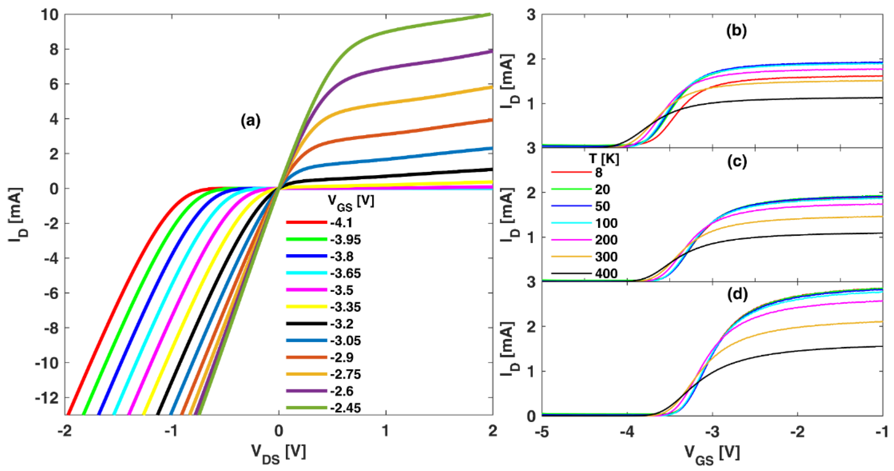
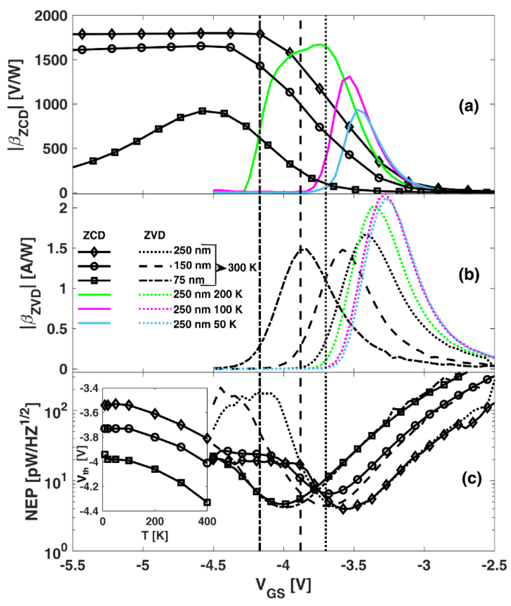
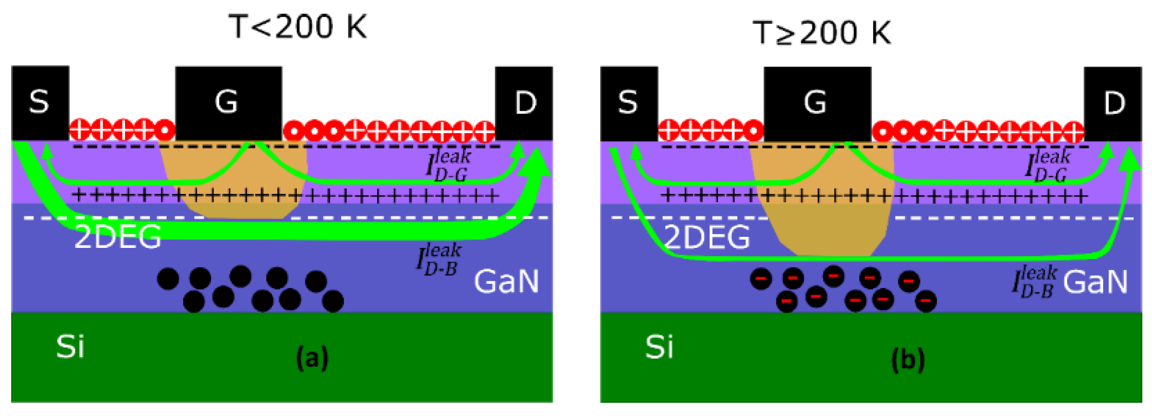
- At T > 200 K, when full ionization is achieved, is strongly suppressed, leading to an improved pinch-off (see Figure 4 for 200 and 300 K) [32,33,34,35,36]. Consequently, the two drain-leakage contributions become of the same order (µA), as sketched in Figure 5b, or even as key:
- ○
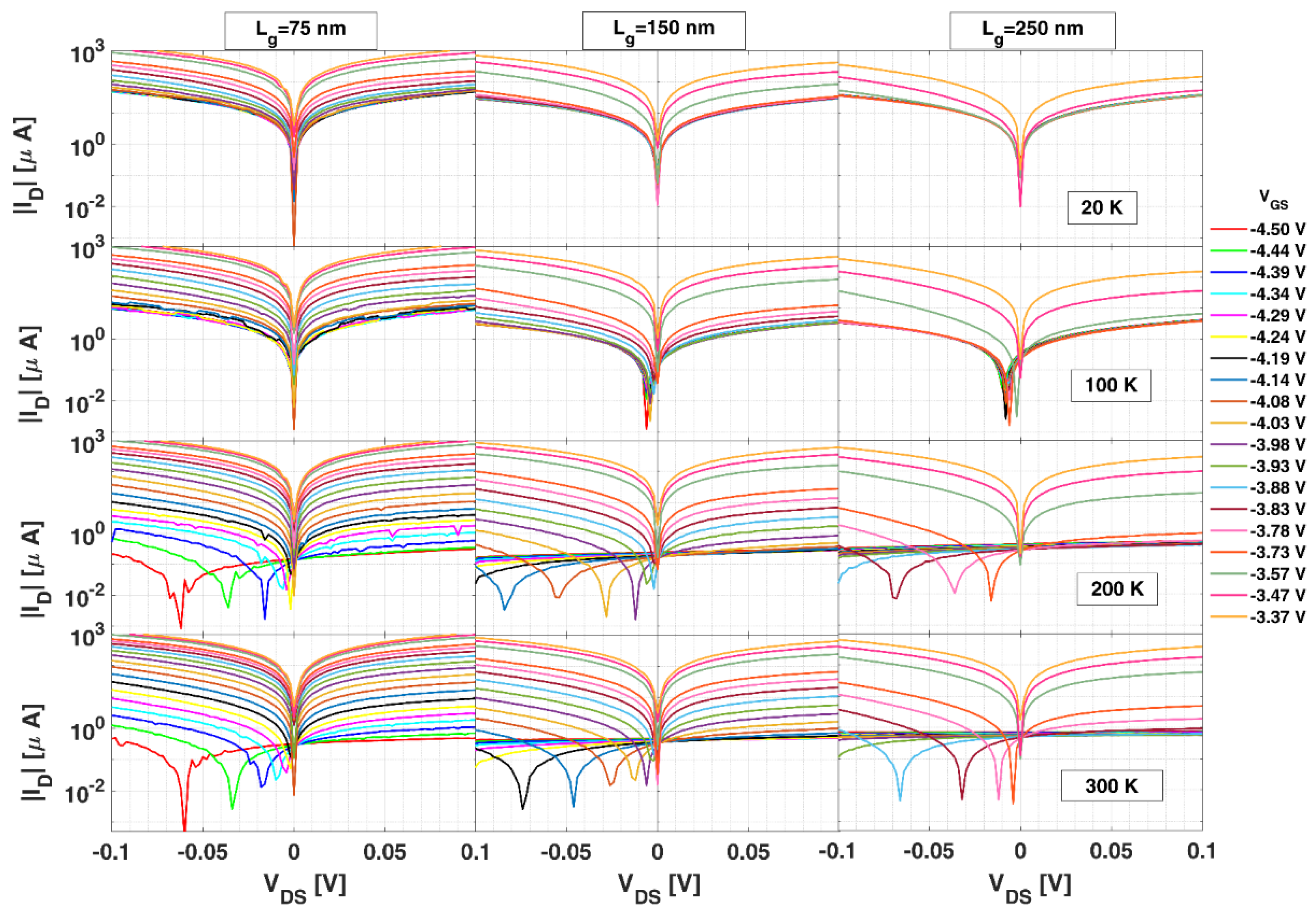
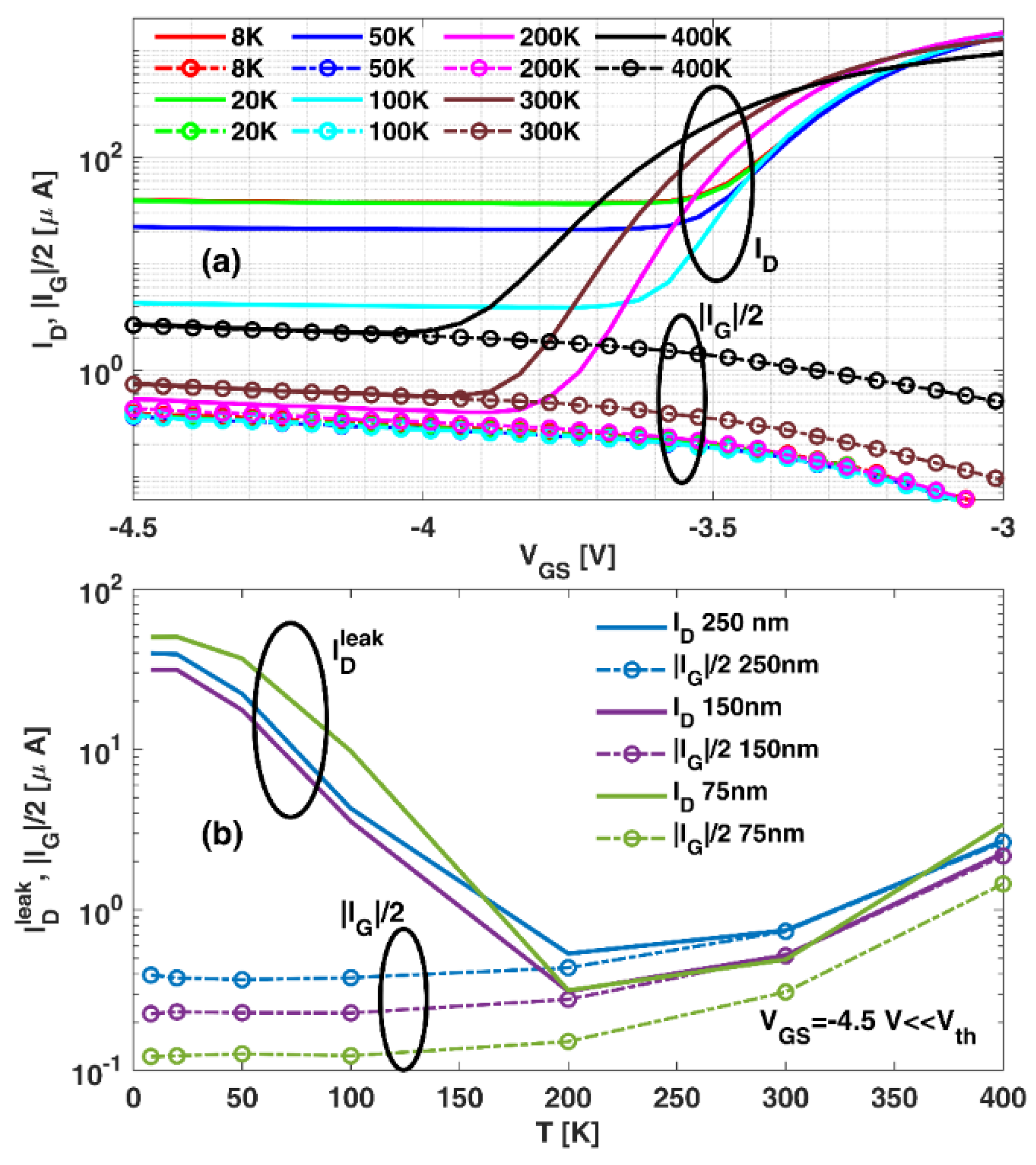
- For Lg = 75 nm, even if is reduced, it is still significant (due to short channel effects) and of the order of , as can be deduced from Figure 6b, where it is observed that > . In such a case, because is positive and almost constant with , the zero- condition is accomplished for a negative value of , for which a negative compensates . As takes higher negative values, decreases and a higher negative value of is necessary to achieve zero current, but not yet reaching the third-quadrant conduction condition. At such a zero- point, the asymmetry of the curves is degraded due to the symmetric contribution of (similarly to what happens at T < 200 K, regardless of the gate length). This is the reason for the decrease in observed at 300 K for this gate length in subthreshold conditions (see Figure 2a);
- ○
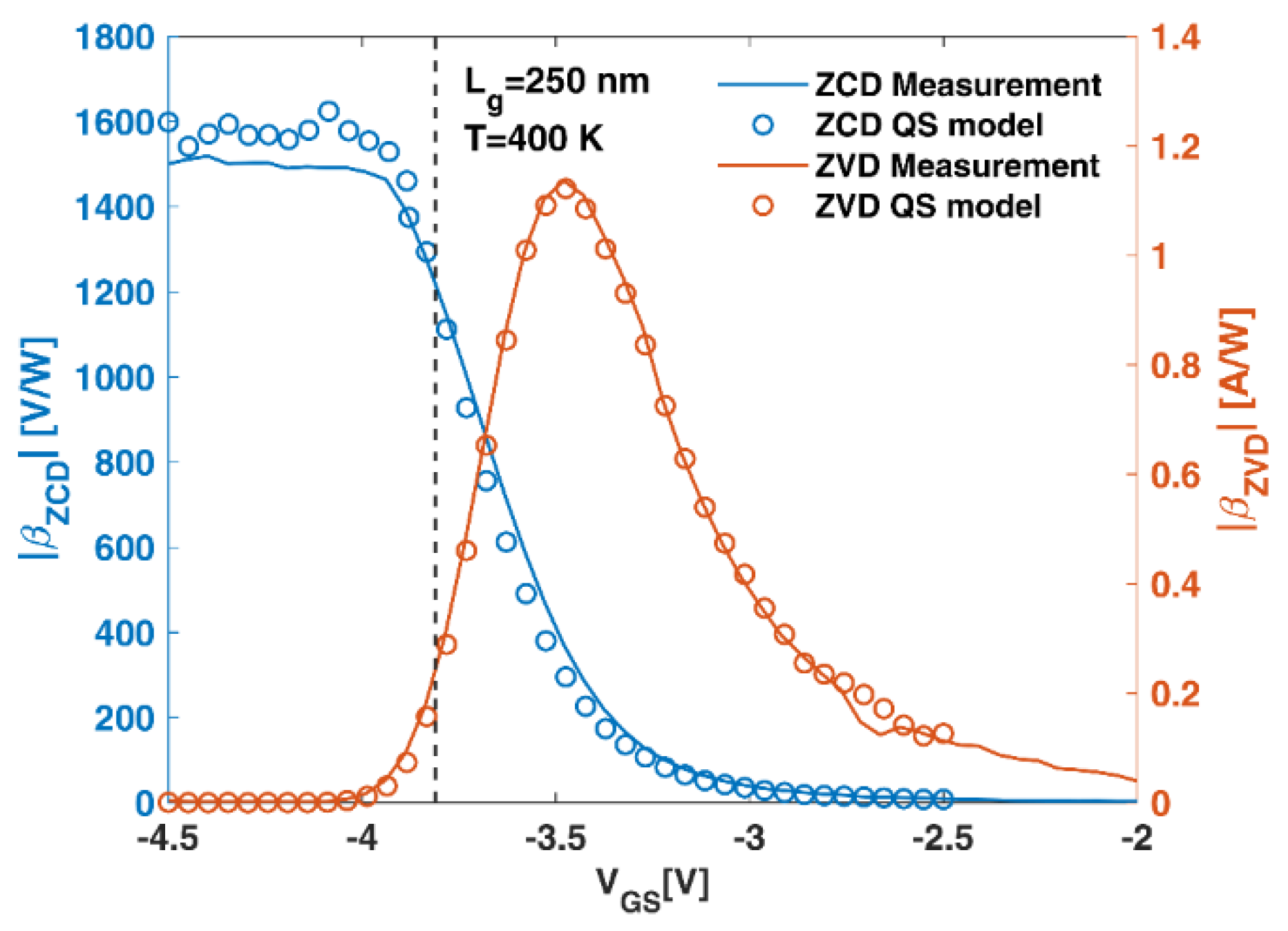
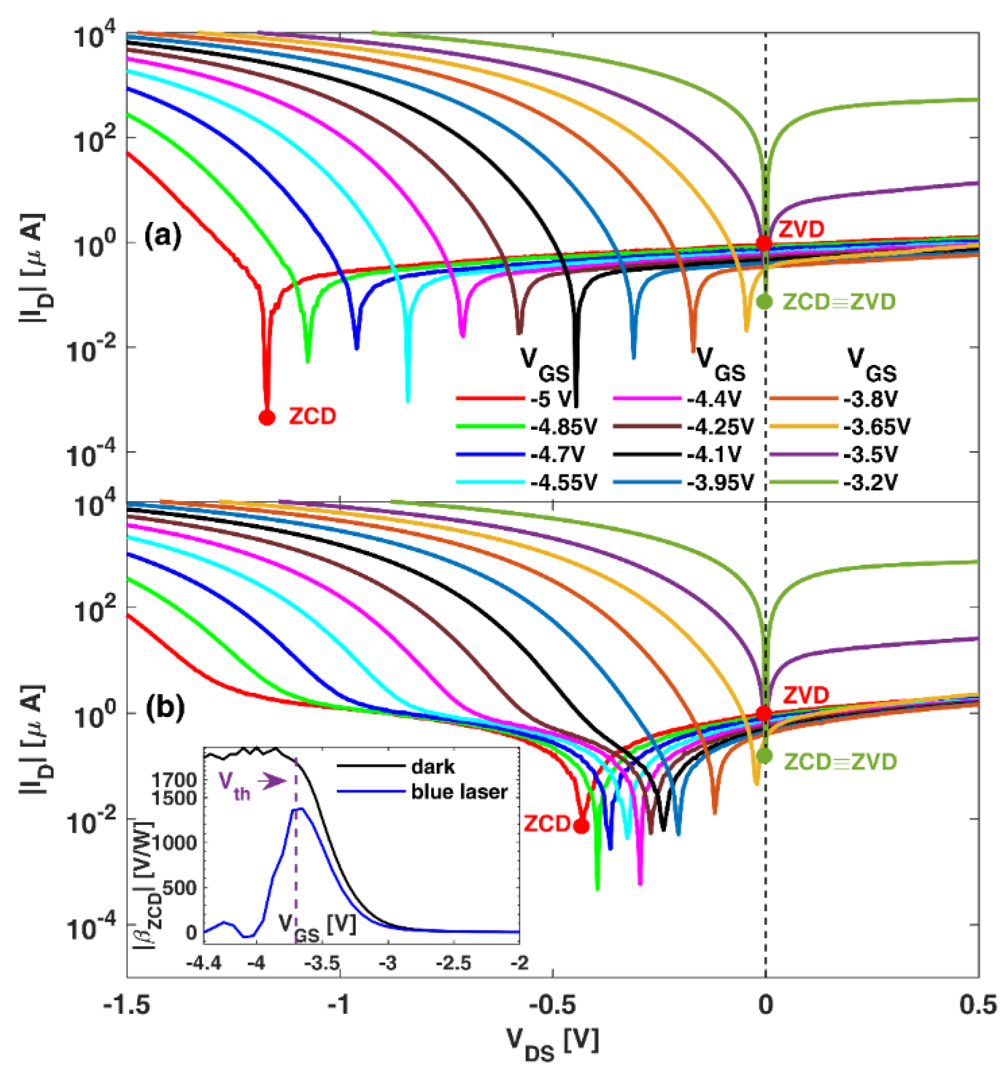
- For long gates = 150 and 250 nm), thanks to the better gate control of the channel concentration (short channel effects are absent in this case), is further reduced and essentially coincides with (Figure 6b). Thus, the zero- point is only achieved when reaches a value near , at which the onset of third-quadrant conduction takes place in the transistor [9,28,29], and the significant increase in (no longer due to buffer leakage but to the opening of the channel for sufficiently negative values of VDS) can compensate . These are the conditions shown in Figure 7a, for = 250 nm and T = 300 K, for which the ZCD operation takes place at a point ( = 0) with strong asymmetry (mainly due to the pronounced increase in once third-quadrant conduction is reached). Consequently, the high value of remains almost constant for < .
4. Conclusions
Author Contributions
Funding
Institutional Review Board Statement
Informed Consent Statement
Data Availability Statement
Conflicts of Interest
References
- Javadi, E.; But, D.B.; Ikamas, K.; Zdanevičius, J.; Knap, W.; Lisauskas, A. Sensitivity of Field-Effect Transistor-Based Terahertz Detectors. Sensors 2021, 21, 2909. [Google Scholar] [CrossRef] [PubMed]
- Stillman, W.; Shur, M.S.; Veksler, D.; Rumyantsev, S.; Guarin, F. Device Loading Effects on Nonresonant Detection of Terahertz Radiation by Silicon MOSFETs. Electron. Lett. 2007, 43, 422. [Google Scholar] [CrossRef]
- Andersson, M.A.; Stake, J. An Accurate Empirical Model Based on Volterra Series for FET Power Detectors. IEEE Trans. Microw. Theory Techn. 2016, 64, 1431–1441. [Google Scholar] [CrossRef] [Green Version]
- Knap, W.; Kachorovskii, V.; Deng, Y.; Rumyantsev, S.; Lü, J.-Q.; Gaska, R.; Shur, M.S.; Simin, G.; Hu, X.; Khan, M.A.; et al. Nonresonant Detection of Terahertz Radiation in Field Effect Transistors. J. Appl. Phys. 2002, 91, 9346–9353. [Google Scholar] [CrossRef]
- Sakowicz, M.; Lifshits, M.B.; Klimenko, O.A.; Schuster, F.; Coquillat, D.; Teppe, F.; Knap, W. Terahertz Responsivity of Field Effect Transistors versus Their Static Channel Conductivity and Loading Effects. J. Appl. Phys. 2011, 110, 054512. [Google Scholar] [CrossRef] [Green Version]
- Hou, H.W.; Liu, Z.; Teng, J.H.; Palacios, T.; Chua, S.J. High Temperature Terahertz Detectors Realized by a GaN High Electron Mobility Transistor. Sci. Rep. 2017, 7, 46664. [Google Scholar] [CrossRef] [PubMed]
- Sánchez-Martín, H.; Mateos, J.; Novoa, J.A.; Delgado-Notario, J.A.; Meziani, Y.M.; Pérez, S.; Theveneau, H.; Ducournau, G.; Gaquière, C.; González, T.; et al. Voltage Controlled Sub-THz Detection with Gated Planar Asymmetric Nanochannels. Appl. Phys. Lett. 2018, 113, 043504. [Google Scholar] [CrossRef]
- Bauer, M.; Ramer, A.; Chevtchenko, S.A.; Osipov, K.Y.; Cibiraite, D.; Pralgauskaite, S.; Ikamas, K.; Lisauskas, A.; Heinrich, W.; Krozer, V.; et al. A High-Sensitivity AlGaN/GaN HEMT Terahertz Detector with Integrated Broadband Bow-Tie Antenna. IEEE Trans. THz Sci. Technol. 2019, 9, 430–444. [Google Scholar] [CrossRef]
- Yasui, T.; Ishikawa, R.; Honjo, K. GaN HEMT DC I–V Device Model for Accurate RF Rectifier Simulation. IEEE Microw. Wirel. Compon. Lett. 2017, 27, 930–932. [Google Scholar] [CrossRef]
- Vitiello, M.S.; Coquillat, D.; Viti, L.; Ercolani, D.; Teppe, F.; Pitanti, A.; Beltram, F.; Sorba, L.; Knap, W.; Tredicucci, A. Room-Temperature Terahertz Detectors Based on Semiconductor Nanowire Field-Effect Transistors. Nano Lett. 2012, 12, 96–101. [Google Scholar] [CrossRef]
- Kojima, H.; Kido, D.; Kanaya, H.; Ishii, H.; Maeda, T.; Ogura, M.; Asano, T. Analysis of Square-Law Detector for High-Sensitive Detection of Terahertz Waves. J. Appl. Phys. 2019, 125, 174506. [Google Scholar] [CrossRef]
- Meneghesso, G.; Verzellesi, G.; Danesin, F.; Rampazzo, F.; Zanon, F.; Tazzoli, A.; Meneghini, M.; Zanoni, E. Reliability of GaN High-Electron-Mobility Transistors: State of the Art and Perspectives. IEEE Trans. Device Mater. Relib. 2008, 8, 332–343. [Google Scholar] [CrossRef]
- del Alamo, J.A.; Joh, J. GaN HEMT Reliability. Microelectron. Reliab. 2009, 49, 1200–1206. [Google Scholar] [CrossRef]
- Zanoni, E.; Meneghini, M.; Chini, A.; Marcon, D.; Meneghesso, G. AlGaN/GaN-Based HEMTs Failure Physics and Reliability: Mechanisms Affecting Gate Edge and Schottky Junction. IEEE Trans. Electron. Devices 2013, 60, 3119–3131. [Google Scholar] [CrossRef]
- Boppel, S.; Lisauskas, A.; Mundt, M.; Seliuta, D.; Minkevicius, L.; Kasalynas, I.; Valusis, G.; Mittendorff, M.; Winnerl, S.; Krozer, V.; et al. CMOS Integrated Antenna-Coupled Field-Effect Transistors for the Detection of Radiation From 0.2 to 4.3 THz. IEEE Trans. Microw. Theory Techn. 2012, 60, 3834–3843. [Google Scholar] [CrossRef]
- Lisauskas, A.; Pfeiffer, U.; Öjefors, E.; Bolìvar, P.H.; Glaab, D.; Roskos, H.G. Rational Design of High-Responsivity Detectors of Terahertz Radiation Based on Distributed Self-Mixing in Silicon Field-Effect Transistors. J. Appl. Phys. 2009, 105, 114511. [Google Scholar] [CrossRef]
- Viti, L.; Cadore, A.R.; Yang, X.; Vorobiev, A.; Muench, J.E.; Watanabe, K.; Taniguchi, T.; Stake, J.; Ferrari, A.C.; Vitiello, M.S. Thermoelectric Graphene Photodetectors with Sub-Nanosecond Response Times at Terahertz Frequencies. Nanophotonics 2020, 10, 89–98. [Google Scholar] [CrossRef]
- Knap, W.; Deng, Y.; Rumyantsev, S.; Shur, M.S. Resonant Detection of Subterahertz and Terahertz Radiation by Plasma Waves in Submicron Field-Effect Transistors. Appl. Phys. Lett. 2002, 81, 4637–4639. [Google Scholar] [CrossRef]
- Rennesson, S.; Lecourt, F.; Defrance, N.; Chmielowska, M.; Chenot, S.; Lesecq, M.; Hoel, V.; Okada, E.; Cordier, Y.; De Jaeger, J.-C. Optimization of Al0.29Ga0.71N/GaN High Electron Mobility Heterostructures for High-Power/Frequency Performances. IEEE Trans. Electron. Devices 2013, 60, 3105–3111. [Google Scholar] [CrossRef]
- Altuntas, P.; Lecourt, F.; Cutivet, A.; Defrance, N.; Okada, E.; Lesecq, M.; Rennesson, S.; Agboton, A.; Cordier, Y.; Hoel, V.; et al. Power Performance at 40 GHz of AlGaN/GaN High-Electron Mobility Transistors Grown by Molecular Beam Epitaxy on Si(111) Substrate. IEEE Electron. Device Lett. 2015, 36, 303–305. [Google Scholar] [CrossRef]
- Sánchez-Martín, H.; García-Pérez, Ó.; Pérez, S.; Altuntas, P.; Hoel, V.; Rennesson, S.; Cordier, Y.; González, T.; Mateos, J.; Íñiguez-de-la-Torre, I. Anomalous DC and RF Behavior of Virgin AlGaN/AlN/GaN HEMTs. Semicond. Sci. Technol. 2017, 32, 035011. [Google Scholar] [CrossRef]
- Choi, Y.C.; Eastman, L.F.; Pophristic, M. Effects of an Fe-Doped GaN Buffer in AlGaN/GaN Power HEMTs on Si Substrate. In 2006 European Solid-State Device Research Conference; IEEE: Montreux, Switzerland, 2006; pp. 282–285. [Google Scholar]
- Zhou, C.; Jiang, Q.; Huang, S.; Chen, K.J. Vertical Leakage/Breakdown Mechanisms in AlGaN/GaN-on-Si Devices. IEEE Electron. Device Lett. 2012, 33, 1132–1134. [Google Scholar] [CrossRef]
- Noh, Y.-K.; Lee, S.-T.; Kim, M.-D.; Oh, J.-E. High Electron Mobility Transistors with Fe-Doped Semi-Insulating GaN Buffers on (1 1 0) Si Substrates Grown by Ammonia Molecular Beam Epitaxy. J. Cryst. Growth 2019, 509, 141–145. [Google Scholar] [CrossRef]
- Bahat-Treidel, E.; Brunner, F.; Hilt, O.; Cho, E.; Wurfl, J.; Trankle, G. AlGaN/GaN/GaN:C Back-Barrier HFETs With Breakdown Voltage of Over 1 KV and Low RON × A. IEEE Trans. Electron. Devices 2010, 57, 3050–3058. [Google Scholar] [CrossRef]
- Cordier, Y.; Semond, F.; Massies, J.; Dessertene, B.; Cassette, S.; Surrugue, M.; Adam, D.; Delage, S.L. AlGaN/GaN HEMTs on Resistive Si(111) Substrate Grown by Gas-Source MBE. Electron. Lett. 2002, 38, 91. [Google Scholar] [CrossRef]
- Cowley, A.M.; Sorensen, H.O. Quantitative Comparison of Solid-State Microwave Detectors. IEEE Trans. Microw. Theory Techn. 1966, 14, 588–602. [Google Scholar] [CrossRef]
- Sorensen, C.; Fogsgaard, M.L.; Christiansen, M.N.; Graungaard, M.K.; Norgaard, J.B.; Uhrenfeldt, C.; Trintis, I. Conduction, Reverse Conduction and Switching Characteristics of GaN E-HEMT. In Proceedings of the 2015 IEEE 6th International Symposium on Power Electronics for Distributed Generation Systems (PEDG), Aachen, Germany, 22–25 June 2015; IEEE: Aachen, Germany, 2015; pp. 1–7. [Google Scholar]
- Sun, B. Does GaN Have a Body Diode?-Understanding the Third Quadrant Operation of GaN. In Application Report SNOAA36; Texas Instruments: Dallas, TX, USA, 2019. [Google Scholar]
- Miller, E.J.; Dang, X.Z.; Yu, E.T. Gate Leakage Current Mechanisms in AlGaN/GaN Heterostructure Field-Effect Transistors. J. Appl. Phys. 2000, 88, 5951–5958. [Google Scholar] [CrossRef] [Green Version]
- Hasegawa, H.; Inagaki, T.; Ootomo, S.; Hashizume, T. Mechanisms of Current Collapse and Gate Leakage Currents in AlGaN/GaN Heterostructure Field Effect Transistors. J. Vac. Sci. Technol. B 2003, 21, 1844. [Google Scholar] [CrossRef] [Green Version]
- Uren, M.; Hayes, D.; Balmer, R.; Wallis, D.; Hilton, K.; Maclean, J.; Martin, T.; Roff, C.; McGovern, P.; Benedikt, J.; et al. Control of Short-Channel Effects in GaN/AlGaN HFETs. In Proceedings of the 2006 European Microwave Integrated Circuits Conference, Manchester, UK, 10–13 September 2006; IEEE: Manchester, UK, 2006; pp. 65–68. [Google Scholar]
- Uren, M.J.; Moreke, J.; Kuball, M. Buffer Design to Minimize Current Collapse in GaN/AlGaN HFETs. IEEE Trans. Electron. Devices 2012, 59, 3327–3333. [Google Scholar] [CrossRef] [Green Version]
- Heikman, S.; Keller, S.; Mates, T.; DenBaars, S.P.; Mishra, U.K. Growth and Characteristics of Fe-Doped GaN. J. Cryst. Growth 2003, 248, 513–517. [Google Scholar] [CrossRef]
- Bisi, D.; Stocco, A.; Rossetto, I.; Meneghini, M.; Rampazzo, F.; Chini, A.; Soci, F.; Pantellini, A.; Lanzieri, C.; Gamarra, P.; et al. Effects of Buffer Compensation Strategies on the Electrical Performance and RF Reliability of AlGaN/GaN HEMTs. Microelectron. Reliab. 2015, 55, 1662–1666. [Google Scholar] [CrossRef] [Green Version]
- Cheney, D.J.; Deist, R.; Gila, B.; Navales, J.; Ren, F.; Pearton, S.J. Trap Detection in Electrically Stressed AlGaN/GaN HEMTs Using Optical Pumping. Microelectron. Reliab. 2012, 52, 2884–2888. [Google Scholar] [CrossRef]
- Mizutani, T.; Ohno, Y.; Akita, M.; Kishimoto, S.; Maezawa, K. Current Collapse in AlGaN/GaN HEMTs Investigated by Electrical and Optical Characterizations. Phys. Stat. Sol. (A) 2002, 194, 447–451. [Google Scholar] [CrossRef]
- Vetury, R.; Zhang, N.Q.; Keller, S.; Mishra, U.K. The Impact of Surface States on the DC and RF Characteristics of AlGaN/GaN HFETs. IEEE Trans. Electron. Devices 2001, 48, 560–566. [Google Scholar] [CrossRef]
- Asubar, J.T.; Yatabe, Z.; Gregusova, D.; Hashizume, T. Controlling Surface/Interface States in GaN-Based Transistors: Surface Model, Insulated Gate, and Surface Passivation. J. Appl. Phys. 2021, 129, 121102. [Google Scholar] [CrossRef]


Publisher’s Note: MDPI stays neutral with regard to jurisdictional claims in published maps and institutional affiliations. |
© 2022 by the authors. Licensee MDPI, Basel, Switzerland. This article is an open access article distributed under the terms and conditions of the Creative Commons Attribution (CC BY) license (https://creativecommons.org/licenses/by/4.0/).
Share and Cite
Paz-Martínez, G.; Íñiguez-de-la-Torre, I.; Sánchez-Martín, H.; Novoa-López, J.A.; Hoel, V.; Cordier, Y.; Mateos, J.; González, T. Temperature and Gate-Length Dependence of Subthreshold RF Detection in GaN HEMTs. Sensors 2022, 22, 1515. https://doi.org/10.3390/s22041515
Paz-Martínez G, Íñiguez-de-la-Torre I, Sánchez-Martín H, Novoa-López JA, Hoel V, Cordier Y, Mateos J, González T. Temperature and Gate-Length Dependence of Subthreshold RF Detection in GaN HEMTs. Sensors. 2022; 22(4):1515. https://doi.org/10.3390/s22041515
Chicago/Turabian StylePaz-Martínez, Gaudencio, Ignacio Íñiguez-de-la-Torre, Héctor Sánchez-Martín, José Antonio Novoa-López, Virginie Hoel, Yvon Cordier, Javier Mateos, and Tomás González. 2022. "Temperature and Gate-Length Dependence of Subthreshold RF Detection in GaN HEMTs" Sensors 22, no. 4: 1515. https://doi.org/10.3390/s22041515
APA StylePaz-Martínez, G., Íñiguez-de-la-Torre, I., Sánchez-Martín, H., Novoa-López, J. A., Hoel, V., Cordier, Y., Mateos, J., & González, T. (2022). Temperature and Gate-Length Dependence of Subthreshold RF Detection in GaN HEMTs. Sensors, 22(4), 1515. https://doi.org/10.3390/s22041515